 | –≠–ª–µ–∫—Ç—Ä–æ–Ω–Ω—ã–π –∫–æ–º–ø–æ–Ω–µ–Ω—Ç: VDEBC2808 | –°–∫–∞—á–∞—Ç—å:  PDF PDF  ZIP ZIP |
V-Data
VDEBC2808
PC-133 SDRAM Unbuffered SO-DIMM
32Mx64bits SDRAM DIMM based on 16Mx16, 4Bank, 8K Refresh, 3.3V SDRAM
General Description
The VDEBC2808 is 32Mx64 bits Synchronous DRAM
Modules, The modules are composed of eight
16Mx16 bits CMOS Synchronous DRAMs in TSOP-II
400mil 54pin package and one 2Kbit EEPROM in 8pin
TSSOP(TSOP) package on a 144pin glass≠epoxy
printed circuit board.
The V-Data is a Dual In-line Memory Module and is
intended for mounting onto 144-pins edge connector
sockets. Fully synchronous operation referenced to
the positive edge of the clock. All inputs and outputs
are synchronized with the rising edge of the clock.
The data paths are internally pipelined to achieve very
high bandwidth.
Features
∑
PC-133 support
∑
Auto refresh and self refresh
∑
8192 refresh cycles / 64ms
∑
Single 3.3±0.3V power supply
∑
All device pins are compatible with LVTTL
interface
∑
Data mask function by DQM
∑
Serial Presence Detect with EEPROM
∑
Module bank : two physical bank
∑
PCB : BSS960,Height (31.75mm),double
sided component, Six layers
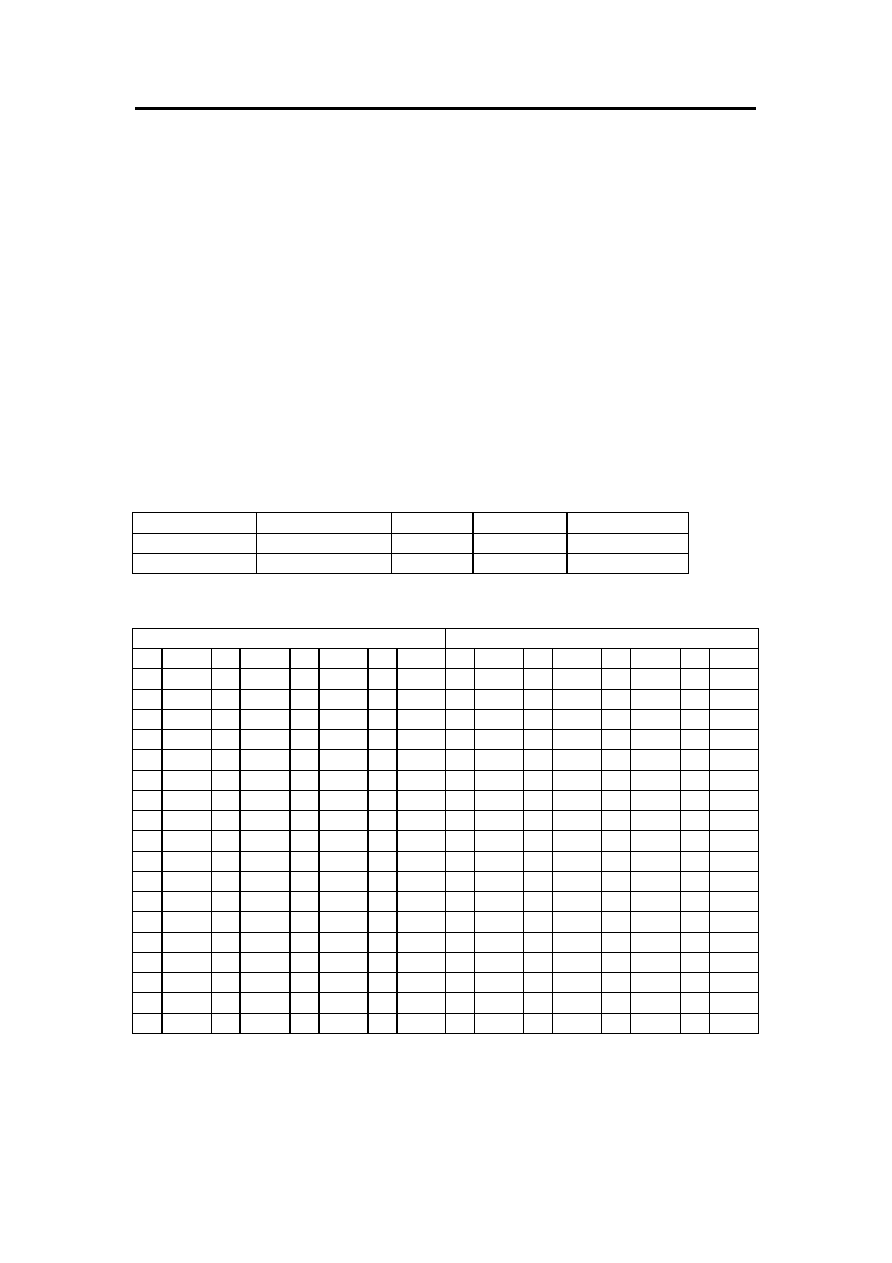
Ordering Information.
Part No.
Frequency
Bank
Ref.
Package
VDEBC2808
133Mhz
4 Banks
8K
TSOP II
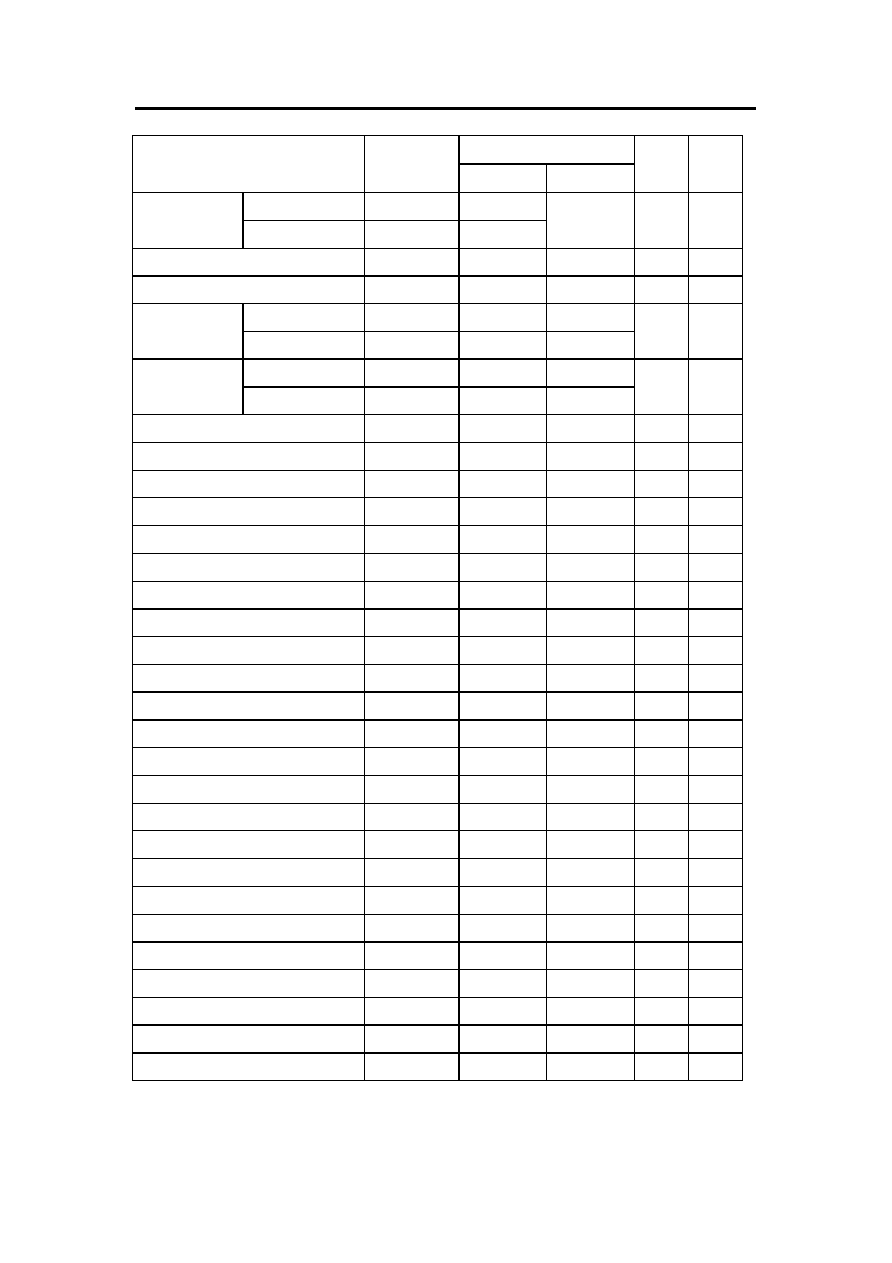
Pin Assignment
FRONT SIDE
BACK SIDE
PIN NAME PIN
NAME
PIN
NAME
PIN NAME PIN NAME PIN NAME PIN NAME
PIN
NAME
1 VSS 19 DQ7 37 DQ8 55
VSS
73
NC 91
VSS 109
A9 127
DQ27
2 VSS 20 DQ39 38 DQ40 56
VSS
74
CK1
92
VSS 110
BA1 128 DQ59
3 DQ0 21 VSS 39 DQ9 57
NC 75
VSS
93 DQ20 111 A10/AP 129 VDD
4 DQ32 22 VSS 40 DQ41 58
NC 76
VSS
94 DQ52 112
A11 130 VDD
5 DQ1 23 DQM0 41 DQ10 59
NC 77
NC 95 DQ21 113 VDD 131 DQ28
6 DQ33 24 DQM4 42 DQ42 60
NC 78
NC 96 DQ53 114 VDD 132 DQ60
7 DQ2 25 DQM1 43 DQ11 61
CK0
79
NC 97 DQ22 115 DQM2 133 DQ29
8 DQ34 26 DQM5 44 DQ43 62 CKE0 80
NC 98 DQ54 116 DQM6 134 DQ61
9 DQ3 27 VDD 45 VDD 63
VDD
81
VDD
99 DQ23 117 DQM3
135
DQ30
10 DQ35 28 VDD 46 VDD 64
VDD
82
VDD 100 DQ55 118 DQM7 136 DQ62
11 VDD 29 A0 47 DQ12 65
/RAS
83 DQ16 101 VDD 119
VSS 137 DQ31
12 VDD 30 A3 48 DQ44 66
/CAS
84 DQ48 102 VDD 120 VSS 138 DQ63
13 DQ4 31 A1 49 DQ13 67
/WE
85 DQ17 103
A6 121 DQ24 139 VSS
14 DQ36 32 A4 50 DQ45 68 CKE1 83 DQ49 104
A7 122 DQ56 140 VSS
15 DQ5 33 A2 51 DQ14 69
/CS0
87 DQ18 105
A8 123 DQ25 141
**SDA
16 DQ37 34 A5 52 DQ46 70
A12
88 DQ50 106 BA0 124 DQ57 142 **SCL
17 DQ6 35 VSS 53 DQ15 71
/CS1
89 DQ19 107 VSS 125 DQ26 143 VDD
18 DQ38 36 VSS 54 DQ47 72
*A13
90 DQ51 108 VSS 126 DQ58 144 VDD
* These pins are not used in this module.
** These pins should be NC in the system which does not support SPD.
Rev 1 April, 2001
1

V-Data
VDEBC2808
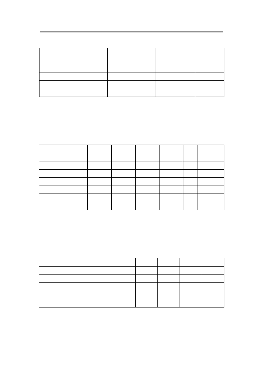
Pin Description
PIN NAME
FUNCTION
CK0~1
System Clock
Active on the positive edge to sample all inputs.
CKE0~1 Clock
Enable
Masks system clock to freeze operation from the next clock cycle. CKE
should be enabled at least on cycle prior new command. Disable input
buffers for power down in standby
/CS0~1 Chip Select
Disables or Enables device operation by masking or enabling all input
except CK, CKE and L(U)DQM
A0~A12 Address
Row / Column address are multiplexed on the same pins.
BA0~BA1 Banks Select
Selects bank to be activated during row address latch time.
Selects bank for read / write during column address latch time.
DQ0~DQ63 Data
Data inputs / outputs are multiplexed on the same pins.
DQM0~7 Data Mask
Makes data output Hi-Z,
/RAS
Row Address Strobe
Latches row addresses on the positive edge of the CLK with /RAS low
/CAS
Column Address Strobe
Latches Column addresses on the positive edge of the CLK with /CAS low
/WE
Write Enable
Enables write operation and row recharge.
VDD/VSS Power Supply/Ground
Power and Ground for the input buffers and the core logic.
SDA
Serial data I/O
EEPROM serial data I/O
SCL
Serial clock
EEPROM clock input
SA0~2
Address in EEPROM
EEPROM address input
NC
No Connection
This pin is recommended to be left No Connection on the device.
Rev 1 April, 2001
2

V-Data
VDEBC2808
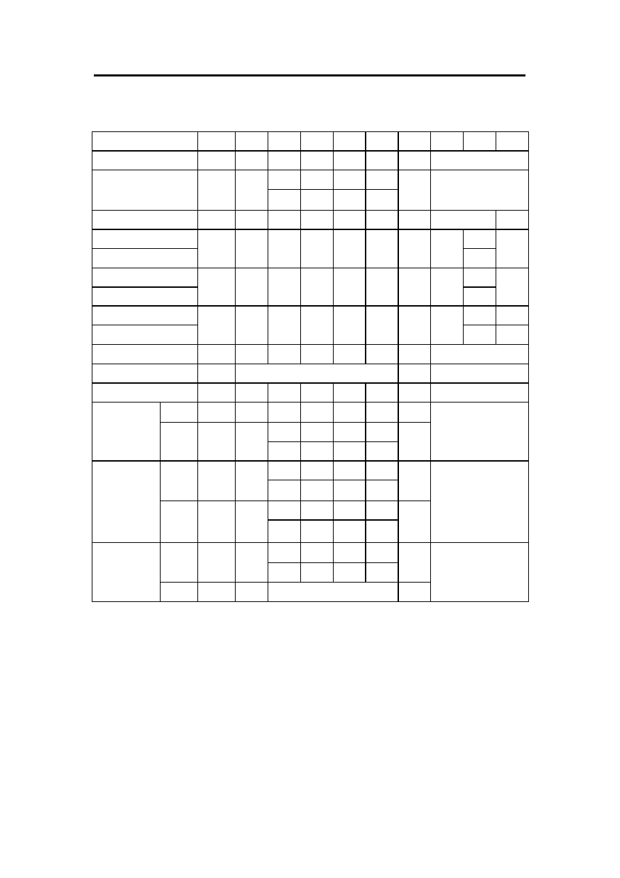
Block Diagram
DQ0
DQ1
DQ2
DQ3
DQ4
DQ5
DQ6
DQ7
DQ8
DQ9
DQ10
DQ11
DQ12
DQ13
DQ14
DQ15
DQ0
DQ1
DQ2
DQ3
DQ4
DQ5
DQ6
DQ7
DQ8
DQ9
DQ10
DQ11
DQ12
DQ13
DQ14
DQ15
DQ0
DQ1
DQ2
DQ3
DQ4
DQ5
DQ6
DQ7
DQ8
DQ9
DQ10
DQ11
DQ12
DQ13
DQ14
DQ15
DQ0
DQ1
DQ2
DQ3
DQ4
DQ5
DQ6
DQ7
DQ8
DQ9
DQ10
DQ11
DQ12
DQ13
DQ14
DQ15
DQ0
DQ1
DQ2
DQ3
DQ4
DQ5
DQ6
DQ7
DQ8
DQ9
DQ10
DQ11
DQ12
DQ13
DQ14
DQ15
DQ16
DQ17
DQ18
DQ19
DQ20
DQ21
DQ22
DQ23
DQ24
DQ25
DQ26
DQ27
DQ28
DQ29
DQ30
DQ31
/CS
/CS
/CS
/CS
LDQM
UDQM
LDQM
UDQM
DQ0
DQ1
DQ2
DQ3
DQ4
DQ5
DQ6
DQ7
DQ8
DQ9
DQ10
DQ11
DQ12
DQ13
DQ14
DQ15
/CS
LDQM
UDQM
DQ0
DQ1
DQ2
DQ3
DQ4
DQ5
DQ6
DQ7
DQ8
DQ9
DQ10
DQ11
DQ12
DQ13
DQ14
DQ15
/CS
LDQM
UDQM
DQ0
DQ1
DQ2
DQ3
DQ4
DQ5
DQ6
DQ7
DQ8
DQ9
DQ10
DQ11
DQ12
DQ13
DQ14
DQ15
/CS
LDQM
UDQM
DQ0
DQ1
DQ2
DQ3
DQ4
DQ5
DQ6
DQ7
DQ8
DQ9
DQ10
DQ11
DQ12
DQ13
DQ14
DQ15
/CS
LDQM
UDQM
LDQM
UDQM
LDQM
UDQM
DQ40
DQ41
DQ42
DQ43
DQ44
DQ45
DQ46
DQ47
DQ48
DQ49
DQ50
DQ51
DQ52
DQ53
DQ54
DQ55
DQ56
DQ57
DQ58
DQ59
DQ60
DQ61
DQ62
DQ63
DQ32
DQ33
DQ34
DQ35
DQ36
DQ37
DQ38
DQ39
/CS1
/CS0
DQM5
DQM4
DQM3
DQM6
DQM7
DQM1
DQM2
DQM0
D0
D4
D1
D3
D7
D5
D6
D2
/RAS
VSS
SCL
SPD
47K Ohms
SA0 SA1 SA2
A0 A1 A2
SDA
WP
VCC
/WE
/CAS
/RAS : D0 ~D7
/WE : D0 ~D7
/CAS : D0 ~D7
A0~A11
BA0/BA1:D0~D7
BA0/BA1
A0~A11:D0~D7
D0~D7
D0~D7
CK : 2 SDRAMs
CK : 2 SDRAMs
CK : 2 SDRAMs
CK : 2 SDRAMs
CKE : D0~D7
CKE0
CK2
CK1
CK3
CK0
3.3 pF
3.3 pF
10 Ohm
10 Ohm
10 Ohm
10 Ohm
Rev 1 April, 2001
3
V-Data
VDEBC2808
Absolute Maximum Ratings
Parameter Symbol
Value
Unit
Voltage on any pin relative to Vss
V
IN
, V
out
-1.0
~
4.6
V
Voltage on VDD supply relative to Vss
V
DD
, V
DDQ
-1.0
~
4.6
V
Storage temperature
T
STG
-55 ~ +150
Power dissipation
P
D
8
W
Short circuit current
I
OS
50
mA
Note : Permanent device damage may occur if ABSOLUTE MAXIMUM RATING are exceeded.
Functional operation should be restricted to recommended operating condition.
Exposure to higher than recommended voltage for extended periods of time could affect device reliability.
DC Operating Condition
Voltage referenced to Vss = 0V, T
A
= 0 to 70
Parameter Symbol
Min
Typ
Max
Unit
Note
Supply voltage
V
DD
, V
DDQ
3.0 3.3 3.6
V
Input logic high voltage
V
IH
2.0 3.0
V
DD
+0.3 V
1
Input logic low voltage
V
IL
-0.3 0 0.8
V 2
Output logic high voltage
V
OH
2.4 -
- V
I
OH
=-2mA
Output logic low voltage
V
OL
- - 0.4
V
I
OL
=2mA
Input leakage current
I
IL
-5 - 5
uA
3
Output leakage current
I
OL
-5 - 5
uA
4
Note : 1. V
IH
(max)=4.6V AC for pulse width 10ns acceptable.
2.V
IL
(min)=-1.5V AC for pulse width 10ns acceptable.
3.Any
input
0V
V
IN
V
DD
+ 0.3V, all other pins are not under test = 0V.
4.Dout is disabled, 0V V
OUT
V
DD
.
AC Operating Condition
Voltage referenced to Vss = 0V, T
A
= 0 to 70
Parameter Symbol
Value
Unit
Note
AC input high / low level voltage
V
IH
/ V
IL
2.4 / 0.4
V
Input timing measurement reference level voltage
Vtrip
1.4
V
Input rise / fall time
TR / tF
1
Ns
Output timing measurement reference level
Voutfef
1.4
V
Output load capacitance for access time measurement
CL
50
pF
2
Note: 1. 3.15V V
DD
3.6V
2. Output load to measure access times is equivalent to two TTL gates and one capacitor (30pF). For details,
refer to AC/DC output load circuit.
Rev 1 April, 2001
4
V-Data
VDEBC2808
Capacitance
TA=25, f-=1Mhz, VDD=3.3V
Parameter Pin
Symbol
Min
Max
Unit
CLK Cl1
25
40
pF
Input capacitance
A0~A11,BA0,BA1,CKE,/CS,/RAS,
/CAS,/WE,DQM
Cl2 40
55
pF
Data input / output capacitance DQM
CI/O
5
15
pF
Output load circuit
V
OH
(DC) = 2.4V,I
OH
= -2mA
V
OL
(DC) = 0.4V,I
OL
= 2mA
3.3 V
1200 ohms
870 ohms
50 pF
Output
DC Characteristics I
Parameter Symbol
Min
Max
Unit
Note
Input leakage current
I
LI
-1
1
uA
1
Output leakage current
I
LO
-1
1
uA
2
Output high voltage
V
OH
2.4
-
V
I
OH
= -4mA
Output low voltage
V
OL
-
0.4
V
I
OL
= 4mA
Note : 1.V
IN
= 0 TO 3.6V, All other pins are not tested under V
IN
= 0V.
2.D
OUT
is disabled, V
OUT
= 0 to 3.6.
Rev 1 April, 2001
5
V-Data
VDEBC2808
DC Characteristics II
Parameter Symbol
Test
condition
Speed
Unit
Note
Operating Current
IDD1
Burst length=1, One bank active
tRCtRC(min),I
OL
=0mA
700 mA
1
IDD2P
CKEV
IL
(max), tCK=min
16
Precharge standby
current in power
down mode
IDD2PS CKEV
IL
(max), tCK=
16
mA
IDD2N
CKEV
IH
(min), /CSV
IH
(min),
tCK=min input signals are
changed one time during 2clks.
All other pins VDD-0.2V or
0.2V
160
Precharge standby
current in Non power
down mode
IDD2NS
CKEV
IH
(min), tCK=
Input signals are stable.
800
mA
IDD3P
CKEV
IL
(max), tCK=min
60
Active standby
current in power
down mode
IDD3PS CKEV
IL
(max), tCK=
60
mA
IDD3N
CKEV
IH
(min), /CSV
IH
(min),
tCK=min input signals are
changed one time during 2clks.
All other pins VDD-0.2V or
0.2V
320
Active standby
current in Non power
down mode
IDD3NS
CKEV
IH
(min), tCK=
Input signals are stable.
320
mA
Burst mode operating
current
IDD4
t
CK
t
CK
(min),I
OL
=0 mA
All banks active
800 mA
1
Auto refresh current IDD5
tRRCtRRC(min), All banks
active
1920 mA
2
Self refresh current
IDD6
CKE0.2V
16 mA
Note: 1. IDD1 and IDD4 depend on output loading and cycle rates. Specified values are measured with the output
open.
2. Min. of tRRC is shown at AC characteristics.
Rev 1 April, 2001
6
V-Data
VDEBC2808
AC Characteristics
VDEBC2808
Parameter Symbol
Min Max
Unit Note
/CAS Latency = 3
tCK3
7.5
System clock
Cycle time
/CAS Latency = 2
tCK2
10
1000 ns
Clock high pulse width
tCHW
2.5
ns
1
Clock low pulse width
tCLW
2.5
ns
1
/CAS Latency = 3
tAC3
5.4
Access time form
clock
/CAS Latency = 2
tAC2
6
ns 2
Operation tRC
65
/RAS cycle time
Auto Refresh
tRRC
65
ns
/RAS to /CAS delay
tRCD
20
ns
/RAS active time
tRAS
45
100K
ns
/RAS precharge time
tRP
20
ns
/RAS to /RAS bank active delay
tRRD
15
ns
/CAS to /CAS delay
tCCD
1
CLK
Write command to data ≠ in delay
tWTL
0
CLK
Data ≠ in to precharge command
tDPL
2
CLK
Data ≠ in active command
tDAL
5
CLK
DQM to data ≠ out Hi-Z
tDQZ
2
CLK
DQM to data ≠ in mask
tDQM
0
CLK
Data ≠ out hold time
tOH
2.7
ns
Data ≠ input setup time
tDS
1.5
ns
1
Data ≠ input hold time
tDH
0.8
ns
1
Address setup time
tAS
1.5
ns
1
Address hold time
tAH
0.8
ns
1
CKE setup time
tCKS
1.5
ns
1
CKE hold time
tCKH
0.8
ns
1
Command setup time
tCS
1.5
ns
1
Command hold time
tCH
0.8
ns
1
CLK to data output in low Z-time
tOLZ
1
ns
MRS to new command
tMRD
2
CLK
Power down exit time
tPDE
1
CLK
Self refresh exit time
tSRE
1
CLK
3
Refresh time
tREF
64
ms
Note : 1. Assume tR / tF (input rise and fall time) is 1 ns.
2. Access times to be measured with input signals of 1v / ns edge rate.
3.A new command can be given tRRC after self refresh exit.
Rev 1 April, 2001
7
V-Data
VDEBC2808
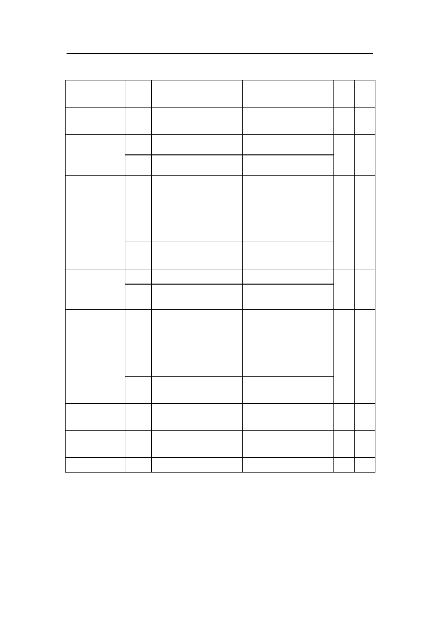
Command Truth-Table
Command CKEn-1
CKEn
/CS
/RAS
/CAS
/WE
DQM
ADDR
A10/AP
BA
Mode
Register
Set
H X L L L L X
OP
code
H X X X
No Operation
H
X
L H H H
X X
Bank Active
H
X
L
L
H
H
X
RA
V
Read
L
Read with Auto Precharge
H X L H L H X CA
H
V
Write
L
Write with Auto Precharge
H X L H L L X CA
H
V
Precharge All Bank
H X
Precharge select Bank
H X L L H L X X
L V
Burst
Stop
H X L H H L X
X
DQM H
X
V
X
Auto
Refresh
H H L L L H X
X
Entry
H L L L L H X
H X X X
Self Refresh
Exit L H
L H H H
X
X
H X X X
Entry
H L
L H H H
X
H X X X
Precharge
Power down
Exit L H
L H H H
X
X
H X X X
Entry
H L
L V V V
X
Clock Suspend
Exit L H
X
X
X
Rev 1 April, 2001
8

V-Data
VDEBC2808
Package Information
2.66
2.50
2-R 0.078 Min
(2.00 Min)
0.18
(4.60)
0.91
(23.20)
1.29
(32.80)
0.
24
(6
.0
)
0.13
0.
79
(2
0
.
0
0
)
(3.30)
(63.60)
(67.56)
Detail Z
0.16
±
0.0039
(4.00
±
0.10)
0.06
±
0.0039
(1.50
±
0.1)
2-
0.07
(1.80)
1.
25
(3
1
.
7
5
)
0.16
±
0.039
(4.00
±
0.10)
0.083
(2.10)
0.10
(2.50)
Z
Y
0.15
(3.70)
0.110 Max
0.04
±
0.0039
(1.00
±
0.10)
0.
12
5
M
i
n
(3
.
2
0
Mi
n
)
(2.40 Max)
0.
1
5
7 M
i
n
(4
.
0
0
Mi
n
)
1
59
61
143
2
6
0
62
144
0.03 TYP
0.024
±
0.001
0.008
±
0.006
(0.200
±
0.150)
(0.600
±
0.050)
(0.80 TYP)
0.
10
0
M
i
n
(2
.
5
4
0
Mi
n
)
Detail Y
Rev 1 April, 2001
9