Advanced Power
N-CHANNEL ENHANCEMENT MODE
Electronics Corp.
POWER MOSFET
Repetitive Avalanche Rated
BV
DSS
700V
Fast Switching Speed
R
DS(ON)
4.4
Simple Drive Requirement
I
D
2.5A
RoHS Compliant
Description
Absolute Maximum Ratings
Symbol
Units
V
DS
Drain-Source Voltage
V
V
GS
Gate-Source Voltage
V
I
D
@T
C
=25
Continuous Drain Current, V
GS
@ 10V
A
I
D
@T
C
=100
Continuous Drain Current, V
GS
@ 10V
A
I
DM
Pulsed Drain Current
1
A
P
D
@T
C
=25
Total Power Dissipation
W
W/
E
AS
Single Pulse Avalanche Energy
2
mJ
I
AR
Avalanche Current
A
T
STG
T
J
Operating Junction Temperature Range
Thermal Data
Symbol
Value
Units
Rthj-c
Thermal Resistance Junction-case
Max.
4.3
/W
Rthj-a
Thermal Resistance Junction-ambient
Max.
65
/W
Data & specifications subject to change without notice
Rating
700
Pb Free Plating Product
AP03N70I-H
2.5
1.6
Storage Temperature Range
-55 to 150
8
29
Linear Derating Factor
0.23
Parameter
2.5
Parameter
-55 to 150
32
200417062-1/4
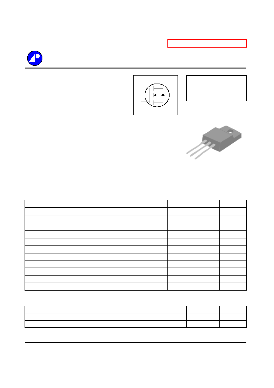
�30
G
D
S
G
D
S
TO-220CFM(I)
AP03N70 series are specially designed as main switching devices for
universal 90~265VAC off-line AC/DC converter applications.
TO-220CFM type provide high blocking voltage to overcome voltage surge
and sag in the toughest power system with the best combination of fast
switching,ruggedized design and cost-effectiveness.

Electrical Characteristics@T
j
=25
o
C(unless otherwise specified)
Symbol
Parameter
Test Conditions
Min.
Typ. Max. Units
BV
DSS
Drain-Source Breakdown Voltage
V
GS
=0V, I
D
=1mA
700
-
-
V
B
V
DSS
/T
j
Breakdown Voltage Temperature Coefficient
Reference to 25
, I
D
=1mA
-
0.6
-
V/
R
DS(ON)
Static Drain-Source On-Resistance
V
GS
=10V, I
D
=1.6A
-
-
4.4
V
GS(th)
Gate Threshold Voltage
V
DS
=V
GS
, I
D
=250uA
2
-
4
V
g
fs
Forward Transconductance
V
DS
=10V, I
D
=1.6A
-
2
-
S
I
DSS
Drain-Source Leakage Current (T
j
=25
o
C)
V
DS
=600V, V
GS
=0V
-
-
10
uA
Drain-Source Leakage Current (T
j
=150
o
C)
V
DS
=480V
,
V
GS
=0V
-
-
100
uA
I
GSS
Gate-Source Leakage
V
GS
=�30V
-
-
�100
nA
Q
g
Total Gate Charge
3
I
D
=1A
-
12
20
nC
Q
gs
Gate-Source Charge
V
DS
=480V
-
3
-
nC
Q
gd
Gate-Drain ("Miller") Charge
V
GS
=10V
-
4
-
nC
t
d(on)
Turn-on Delay Time
3
V
DD
=300V
-
8.5
-
ns
t
r
Rise Time
I
D
=2.5A
-
6
-
ns
t
d(off)
Turn-off Delay Time
R
G
=10
,
V
GS
=10V
-
19
-
ns
t
f
Fall Time
R
D
=120
-
8
-
ns
C
iss
Input Capacitance
V
GS
=0V
-
590
950
pF
C
oss
Output Capacitance
V
DS
=25V
-
50
-
pF
C
rss
Reverse Transfer Capacitance
f=1.0MHz
-
6
-
pF
Source-Drain Diode
Symbol
Parameter
Test Conditions
Min.
Typ. Max. Units
V
SD
Forward On Voltage
3
I
S
=3A, V
GS
=0V
-
-
1.5
V
t
rr
Reverse Recovery Time
2
I
S
=3A, V
GS
=0V,
-
407
-
ns
Q
rr
Reverse Recovery Charge
dI/dt=100A/�s
-
2110
-
nC
Notes:
1.Pulse width limited by safe operating area.
2.Starting T
j
=25
o
C , V
DD
=50V , L=15mH , R
G
=25
, I
AS
=3A.
3.Pulse width <300us , duty cycle <2%.
AP03N70I-H
2/4

Fig 1. Typical Output Characteristics
Fig 2. Typical Output Characteristics
Fig 3. Normalized BV
DSS
v.s. Junction
Fig 4. Normalized On-Resistance
Temperature
v.s. Junction Temperature
Fig 5. Forward Characteristic of
Fig 6. Gate Threshold Voltage v.s.
Reverse Diode
Junction Temperature
3/4
AP03N70I-H
0
1
2
3
4
0
5
10
15
20
25
V
DS
, Drain-to-Source Voltage (V)
I
D
, Dr
a
i
n C
u
r
r
e
nt
(A
)
T
C
=25
o
C
5.0V
4.5V
V
G
=4.0V
10V
6.0V
0
1
1
2
2
3
0
5
10
15
20
25
V
DS
, Drain-to-Source Voltage (V)
I
D
, Dr
a
i
n C
u
r
r
e
nt
(A
)
T
C
=150
o
C
V
G
=3.5V
4.5V
4.0V
10V
5.0V
0.0
1.0
2.0
3.0
-50
0
50
100
150
T
j
, Junction Temperature (
o
C)
N
o
rmalize
d
R
DS(ON)
I
D
=1.6A
V
G
=10V
0.8
0.9
1.0
1.1
1.2
-50
0
50
100
150
T
j
, Junction Temperature (
o
C)
N
o
rmalize
d
BV
DSS
(V
)
0.01
0.1
1
10
100
0.1
0.3
0.5
0.7
0.9
1.1
1.3
V
SD
, Source-to-Drain Voltage (V)
I
S
(A
)
T
j
= 25
o
C
T
j
= 150
o
C
1
2
3
4
5
-50
0
50
100
150
T
j
, Junction Temperature (
o
C)
V
GS(t
h)
(V
)

AP03N70I-H
Fig 7. Gate Charge Characteristics
Fig 8. Typical Capacitance Characteristics
Fig 9. Maximum Safe Operating Area
Fig 10. Effective Transient Thermal Impedance
Fig 11. Switching Time Waveform
Fig 12. Gate Charge Waveform
4/4
0.01
0.1
1
0.00001
0.0001
0.001
0.01
0.1
1
10
t , Pulse Width (s)
N
o
rmalize
d
T
h
e
rmal Re
spon
se
(
R
th
jc
)
P
DM
Duty factor = t/T
Peak T
j
= P
DM
x R
thjc
+ T
C
t
T
0.02
0.01
0.05
0.1
0.2
Duty factor=0.5
Single Pulse
t
d(on)
t
r
t
d(off)
t
f
V
DS
V
GS
10%
90%
Q
V
G
10V
Q
GS
Q
GD
Q
G
Charge
0
4
8
12
16
0
4
8
12
16
Q
G
, Total Gate Charge (nC)
V
GS
,
G
a
te
to S
o
u
rc
e
Voltage
(
V
)
I
D
=1A
V
DS
=480V
1
100
10000
1
5
9
13
17
21
25
29
V
DS
, Drain-to-Source Voltage (V)
C (
p
F)
f=1.0MHz
C
iss
C
oss
C
rss
0.01
0.1
1
10
1
10
100
1000
10000
V
DS
, Drain-to-Source Voltage (V)
I
D
(A
)
10us
100us
1ms
10ms
100ms
T
c
=25
o
C
Single Pulse