Advanced Power
N-CHANNEL INSULATED GATE
Electronics Corp.
BIPOLAR TRANSISTOR
High Input Impedance
V
CE
High Pick Current Capability
I
CP
3.3V Gate Drive
Strobe Flash Applications
Absolute Maximum Ratings
Electrical Characteristics@T
j
=25
o
C(unless otherwise specified)
Symbol
Min.
Typ.
Max. Units
I
GES
-
-
10
uA
I
CES
-
-
10
uA
V
CE(sat)
-
3.8
6
V
V
GE(th)
-
-
1
V
Q
g
-
74
120
nC
Q
ge
-
8
-
nC
Q
gc
-
34
-
nC
t
d(on)
-
20
-
ns
t
r
-
100
-
ns
t
d(off)
-
400
-
ns
t
f
-
3
-
�
s
C
ies
-
3020 4830
pF
C
oes
-
220
-
pF
C
res
-
50
-
pF
Rth
JA
1
-
-
50
/W
Notes:
1.Surface mounted on 1 in
2
copper pad of
FR4 board ; 125
/W when mounted on Min. copper pad.
Data and specifications subject to change without notice
Thermal Resistance Junction-Ambient
V
GE
=4.5V
Fall Time
Input Capacitance
Output Capacitance
f=1.0MHz
V
GE
=� 6V, V
CE
=0V
T
STG
Turn-off Delay Time
V
GE
=0V
I
C
=15A
R
G
=10
Rise Time
T
J
Gate-Collector Charge
Turn-on Delay Time
Collector-Emitter Saturation Voltage
Gate Threshold Voltage
Total Gate Charge
Gate-Emitter Leakage Current
Collector-Emitter Leakage Current
A
Reverse Transfer Capacitance
V
CE
=450V, V
GE
=0V
V
GE
=3.3V, I
CP
=130A (Pulsed)
V
CE
=V
GE
, I
C
=250uA
I
C
=40A
V
CE
=360V
V
GE
=5V
V
CE
=25V
Test Conditions
AP28G45GEM
Symbol
V
CE
450V
130A
Rating
Collector-Emitter Voltage
Units
V
450
� 6
130
� 8
Parameter
Storage Temperature Range
Pulsed Collector Current, V
GE
@ 3.3V
Parameter
Maximum Power Dissipation
V
GE
I
CP
I
GEP
Pulsed Gate-Emitter Voltage
P
D
@T
C
=25
1
Operating Junction Temperature Range
-55 to 150
-55 to 150
W
Pb Free Plating Product
V
2.5
201117031
V
CC
=200V
V
Gate-Emitter Voltage
Gate-Emitter Charge
G
C
E
E
E
E
G
C
C
C
C
SO-8
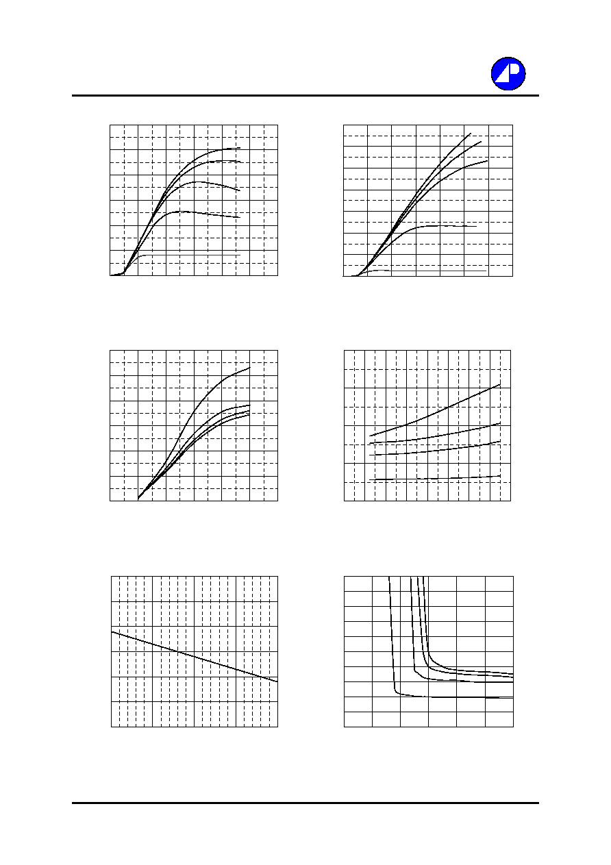
Fig 1. Typical Output Characteristics
Fig 2. Typical Output Characteristics
Fig 3. Collector Current v.s.
Fig 4. Collector- Emitter Saturation Voltage
Gate-Emitter Voltage
v.s. Junction Temperature
Fig 5. Gate Threshold Voltage
Fig 6. Collector Current v.s.
v.s. Junction Temperature
Gate-Emitter Voltage
AP28G45GEM
0.0
0.2
0.4
0.6
0.8
1.0
1.2
-50
0
50
100
150
Junction Temperature (
o
C )
V
GE
(t
h)
,
G
ate
Th
re
sh
old V
o
ltage
(
V
)
1
3
5
7
9
0
20
40
60
80
100
120
140
160
Junction Temperature (
o
C)
V
CE(
s
a
t
)
,
S
atu
r
ation
V
o
ltage
(
V
)
V
GE
=4.0V
I
C
=120A
I
C
=50A
I
C
=100A
I
C
=130A
0
20
40
60
80
100
120
140
0
1
2
3
4
5
6
7
V
CE
, Collector-Emitter Voltage (V)
I
C
, C
o
l
l
ect
o
r
C
u
r
r
e
nt
(A
)
T
A
= 150
o
C
5.0V
4.0V
3.3 V
2.0V
V
G
=1.0V
0
40
80
120
160
200
240
0
2
4
6
8
10
12
V
CE
, Collector-Emitter Voltage (V)
I
C
, C
o
l
l
ect
o
r
C
u
r
r
e
nt
(A
)
T
A
=25
o
C
5.0V
4.0V
3.3V
2.0V
V
G
=1.0V
0
2
4
6
8
10
0
1
2
3
4
5
6
V
GE
, Gate-Emitter Voltage(V)
V
CE
,
C
olle
c
t
or-
E
mitte
r Voltage
(
V
)
I
C
= 130 A
120A
100A
50A
T
A
=25
o
C
0
40
80
120
160
200
240
0
1
2
3
4
5
6
V
GE
, Gate-Emitter Voltage (V)
I
C
,
Co
lle
c
t
o
r
Cu
rre
n
t
(
A
)
V
CE
=6.0V
25
o
C
70
o
C
125
o
C
T
A
=150
o
C

Fig 7. Typical Capacitance Characterisitics Fig 8. Maximum Pulse Collector Current
Fig 9. Switching Time Test Circuit
Fig 10. Switching Time Waveform
Fig 11. Gate Charge Test Circuit
Fig 12. Gate Charge Waveform
AP28G45GEM
t
d(on)
t
r
t
d(off)
t
f
V
CE
V
GE
10%
90%
TO THE
OSCILLOSCOPE
-
+
5V
C
G
E
V
CE
V
GE
R
G
R
C
V
CC
=200 V
10
100
1000
10000
1
5
9
13
17
21
25
29
V
CE
, Collector-Emitter Voltage (V))
C (
p
F)
f=1.0MHz
Cies
Coes
Cres
V
CC
=360V
TO THE
OSCILLOSCOPE
-
+
C
G
V
CE
V
GE
I
C
I
G
1~3mA
E
0
2
4
6
8
10
12
0
40
80
120
160
200
Q
G
, Gate Charge (nC)
V
GE
,
G
a
te
-
E
mitte
r Voltage
(
V
)
I
CP
=40A
V
CE
=360V
0
40
80
120
160
0
2
4
6
8
V
GE
, Gate-to-Emitter Voltage (V)
I
CP
,
Pe
ak C
o
lle
c
t
or C
u
rre
n
t
(
A
)
T
A
=25
o
C