Advanced Analog Technology, Inc.
≠
≠
≠
Advanced Analog Technology, Inc
.
≠
Page 1 of 21 V 1.0
AAT1201
Details are subject to change without notice
250-mA MULTI-INPUT LOW-DROPOUT REGULATOR
WITH DUAL-OUTPUT POWER MANAGEMENT
Features
Complete Power Management
Automatic Input Voltage Selection
Input Voltage Source Detector with Hysteresis
250-mA Load Current Capability with
VCC50 or VSB50 or AUX33 Input Source
Integrated Low
( )
on
DS
r
Switch
Dual Regulated Output 3.3V (fixed) & 2.5V
(fixed)
Output Short Circuit Protection (SCP)
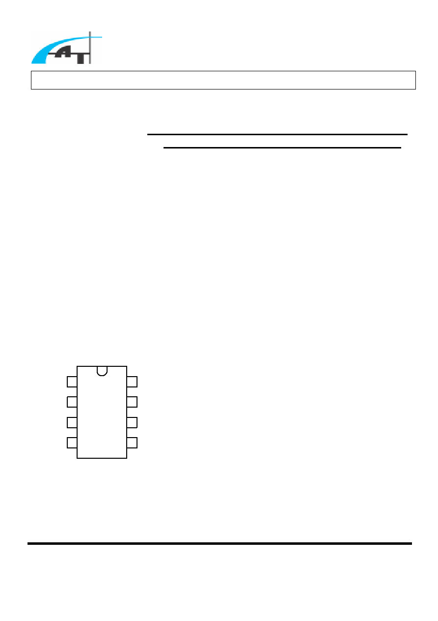
Pin Configuration
Description
The AAT1201 is a multi-input low-dropout
regulator (LDO) designed for LAN card. It
provides dual constant output supply 3.3V & 2.5V
at the output capable of driving a 250-mA load.
The output (OUT25) can be disabled by
connecting EN25 pin to GND.
The AAT1201 provides dual regulated power
output for systems with multiple input sources and
require dual constant voltage source with a
low-dropout voltage. This is an intelligent power
source selection device with a LDO regulator for
either VCC50 or VSB50 inputs, and a
low-resistance bypass switch for the AUX33
input.
The AAT1201 allows transitions to progress
smoothly from one input supply to another without
generating a glitch outside of the specified range
of the 3.3-V & 2.5-V output. The device is
equipped with an incorporated reverse-blocking
scheme to prevent excess leakage from the input
terminals in the event when the output voltage is
greater than the input voltage.
The input voltage is prioritized in the following
order: VCC50, VSB50, AUX33.
VSB50
VCC50
OUT33
AUX33
GND
GND
EN25
OUT25
1
2
3
4
8
7
6
5
( 8-PIN SOP )
TOP VIEW
Advanced Analog Technology, Inc.
≠
≠
≠
Advanced Analog Technology, Inc
.
≠
Page 2 of 21 V 1.0
AAT1201
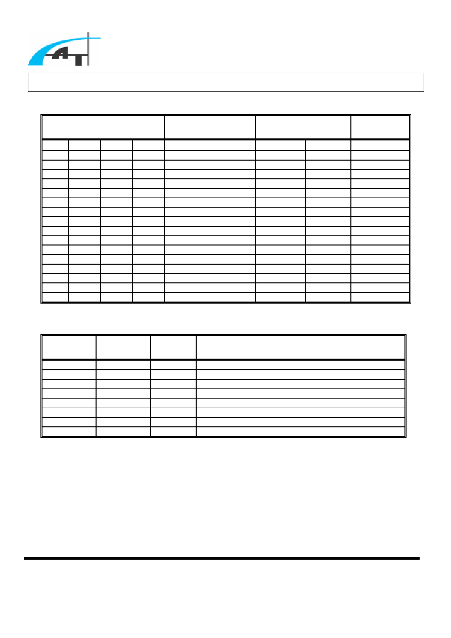
Function Table
INPUT VOLTAGE STATUS
(V)
INPUT SELECTED
OUTPUTV
OUTPUT
ImA
EN25 VCC50 VSB50 AUX33 VCC50/VSB50/AUX33
OUT33
OUT25 Iout33+Iout25
Hi 0 0 0
None
0
0
0
Lo
0 0 0
None
0
0
0
Hi 0 0 3.3
AUX33
3.3
2.5
250
Lo
0
0
3.3 AUX33
3.3 0 250
Hi 0 5 0
VSB50
3.3
2.5
250
Lo
0 5 0
VSB50
3.3
0
250
Hi 0 5.0 3.3
VSB50
3.3
2.5
250
Lo 0 5.0 3.3
VSB50
3.3
0
250
Hi 5 0 0
VCC50
3.3
2.5
250
Lo
5 0 0
VCC50
3.3
0
250
Hi 5 0 3.3
VCC50
3.3
2.5
250
Lo 5 0 3.3
VCC50
3.3
0
250
Hi 5 5 0
VCC50
3.3
2.5
250
Lo
5 5 0
VCC50
3.3
0
250
Hi 5.0 5.0 3.3
VCC50
3.3
2.5
250
Lo 5.0 5.0 3.3
VCC50
3.3
0
250
Pin Description
TERMINAL
NAME
TERMINAL
NO.
I/O Description
VSB50
1
I
5V Standby Supply Input
VCC50
2
I
5V Main Supply Input
OUT33
3
O
3.3V Regulated Output
AUX33
4
I
3.3V Auxiliary Supply Input
OUT25
5
O
2.5V Regulated Output
EN25
6
I
Enable Input of OUT25
GND
7
I
Ground
GND
8
I
Ground
Advanced Analog Technology, Inc.
≠
≠
≠
Advanced Analog Technology, Inc
.
≠
Page 3 of 21 V 1.0
AAT1201
Absolute Maximum Ratings
∑ Main Supply Voltage,
(
)
50
VCC
V
..............................................................
5
.
0
-
V~7V
∑ Standby Supply Voltage,
(
)
50
VSB
V
............................................................
5
.
0
-
V~7V
∑ Auxiliary Supply Voltage,
(
)
33
AUX
V
..........................................................
5
.
0
-
~7V
∑ Output Current Limit,
(
)
LIMIT
I
................................................................1.5A
∑ Continuous Power Dissipation,
d
P see Note 1...................................... 1.1W
∑ Electrostatic Discharge Susceptibility, Human Body Mode..............................2kV
∑ Operating Free-Air Temperature Range,
C
T ..............................................0 to
+70
∑ Storage Temperature Range,
storage
T
.......................................................
45
-
to
+125
∑ Operating Junction Temperature Range,
J
T ...............................................
5
-
to
+130
∑ Lead TemperatureSoldering for 10 seconds,
(
)
LEAD
T
..............................260
Note 1
The device deteriorates with increase in ambient temperature,
C
T
. See Thermal Information section.
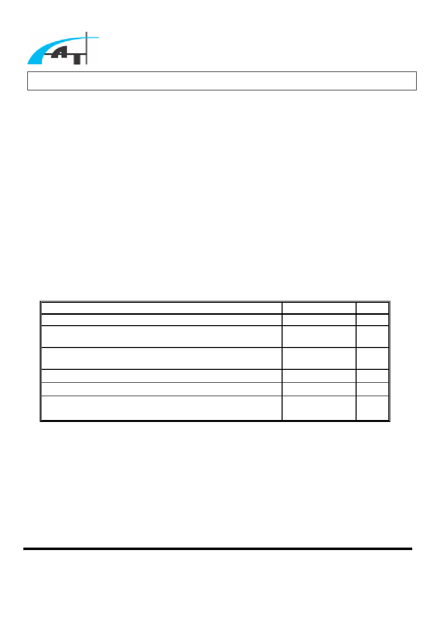
Recommended Operating Conditions
Parameter Min Typ
Max
Unit
5V Main Supply Input, VCC50
4.5
-
5.5
V
5V Standby Supply Input,
VSB50
4.5 - 5.5 V
3.3V Auxiliary Supply Input,
AUX33
3.0 - 3.6 V
Load Capacitance,
L
C
4.23 4.70 5.17 µF
Load Current,
L
I
0 -
250
mA
Operating Free-Air Temperature,
C
T
0 - 70

Advanced Analog Technology, Inc.
≠
≠
≠
Advanced Analog Technology, Inc
.
≠
Page 4 of 21 V 1.0
AAT1201
Electrical Characteristics Over Recommended Operating Free-Air Temperature, T
C
=
0 to 70 ,
L
C
= 4.7µF (unless otherwise specified)
Parameter Symbol Test
Condition Min
Typ
Max
Unit
5V Inputs
VCC50
VSB50
4.5 5.0 5.5 V
3.3V Output
OUT33
33
out
I
+
25
out
I
= 250mA
3.135 3.300 3.465 V
2.5V Output
OUT25
33
out
I
=0,
25
out
I
= 200mA
2.375 2.500 2.625 V
Line Regulation Voltage
(
)
VI
O
V
VSB50 or VCC50 = 4.5V to 5.5V
-
2
-
mV
Load Regulation Voltage
(
)
IO
O
V
20 mAI
L
250 mA
- 40 - mV
Quiescent Supply Current
50
I
From VCC50 VSB50 Terminals,
L
I = 0 to 250mA
- 1.0 3.0
mA
AUX
I
From AUX33 Terminal,
L
I = 0A
- 1.0 3.0
mA
Out33 Load Current
33
L
I
0.25
-
-
Out25 Load Current
25
L
I
0.2
-
-
Output Current Limit
LIMIT
I
Out33 or Out25 Output Shortened to
0V
- - 1.5
A
Thermal Shutdown
(Note 2)
TSD
T
150 - 180
Thermal Hysteresis
(Note 2)
hys
T
- 15 -
Load Capacitance
L
C
Minimal ESR to Insure Stability of
Regulated Output
- 4.7 - µF
Reverse Leakage Output
Current
(
)
REV
Ikg
I
Tested for Grounded Input
AUX33, VSB50 or VCC50 = GND,
Out33 = 3.3V
- - 50
µA
Threshold Voltage, Low
LO
V
VSB50 or VCC50
3.85 4.05 4.25 V
Threshold Voltage, High
HI
V
VSB50 or VCC50
4.1 4.3 4.5 V
Auxiliary Switch
Resistance
SWITCH
R
VSB50 = VCC50 = 0V,
AUX33 = 3.3V,
L
I = 150mA
- - 0.4
Without Copper for Heat Spreading
-
100
-
Thermal Impedance,
Junction-to-Ambient
(Note 3)
JA
R
With Copper for Heat Spreading
-
70
-
/W
Note 2
Design targets only. Not tested in production.
Note 3Please refer to "Thermal Information"

Advanced Analog Technology, Inc.
≠
≠
≠
Advanced Analog Technology, Inc
.
≠
Page 5 of 21 V 1.0
AAT1201
Block Diagram