Advanced Analog Technology, Inc.
≠
≠
≠
Advanced Analog Technology, Inc
.
≠
Page 1 of 14 V1.0
AAT1343
Details are subject to change without notice
2-CHANNEL SWITCHING REGULATOR
FEATURES
Complete PWM Power Control Circuitry
Precision Reference2.5V ± 1% (25
o
C)
Under-Voltage Lockout (UVLO) Protection
Open Drain Output
Output Short Circuit Protection
Low Dissipation Current1.6mA
Dead-Time Control0 % to 100%
Wide Operating Frequency
10kHz to 800kHz
DD
V
Range4.0V to 14.0V
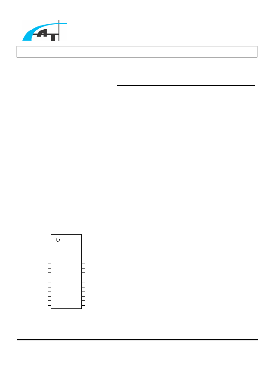
PIN CONFIGURATION
1
2
3
4
5
6
7
8
16
15
14
13
12
11
10
9
IE1
OE1
DTC1
GND
OUT1
V
REF
NE2
SCP
IE2
OE2
DTC2
OUT2
TOP VIEW
NE1
V
DD
TSSOP-16 PACKAGE
R
t
C
t
GENERAL DESCRIPTION
The AAT1343 provides an integrated two-channel
pulse-width-modulation (PWM) solution for the
power supply of DC-DC system; this device offers
the systems engineer flexibility to tailor-make the
power supply circuitry for specific applications.
Each channel contains its own error amplifier,
PWM comparator, dead≠time control (DTC) and
output driver. The under-voltage protection,
oscillator, short circuit protection and voltage
reference circuit are the common features for these
two channels.
Both channels of AAT1343 can be used for DC-DC
converter operations including step-up, step-down,
and inverting. Dead-time control can be set to
provide 0% to 100% dead-time through a resistive
divider network. Soft-start can be implemented by
paralleling the DTC resistor with a capacitor. Two
dead-time control inputs are assigned for channel 1
(CH1) and channel 2 (CH2) individually, and
dead-time control inputs can be used to control on /
off operation.
With a minimal number of external components, the
AAT1343 offers a simple and cost effective
solution.

Advanced Analog Technology, Inc.
≠
≠
≠
Advanced Analog Technology, Inc
.
≠
Page 2 of 14 V1.0
AAT1343
PIN DESCRIPTION
PIN NO. NAME I/O
DESCRIPTION
1
t
C
I External Timing Capacitor
2
t
R
I External Timing Resistor
3 NE1
I
Noninverting Input of Error Amplifier 1
4
IE1
I Inverting Input of Error Amplifier 1
5
OE1
I Output of Error Amplifier 1
6
DTC1
I Output 1 Dead-Time / Soft-Start Setting
7 OUT1
O
Output
1
8 GND
Ground
9 V
DD
I
Power
Supply
10 OUT2
O
Output
2
11
DTC2
I Output 2 Dead-Time / Soft-Start Setting
12
OE2
I Output of Error Amplifier 2
13
IE2
I Inverting Input of Error Amplifier 2
14 NE2
I
Noninverting Input of Error Amplifier 2
15
SCP
I Timer Latch Setting
16
REF
V
O Reference Voltage (2.5V) Output

Advanced Analog Technology, Inc.
≠
≠
≠
Advanced Analog Technology, Inc
.
≠
Page 3 of 14 V1.0
AAT1343
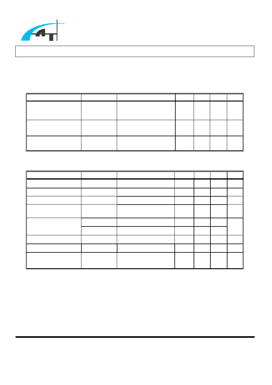
ABSOLUTE MAXIMUM RATINGS
CHARACTERISTICS SYMBOL
VALUE
UNIT
Supply Voltage
DD
V
14.0 V
Input Voltage (
-
IE
, DTC)
I
V
DD
V
V
Output Voltage
O
V
DD
V +0.3
V
Output Current
O
I
120 mA
Operating Free-Air Temperature Range
C
T
20
-
to
85
+
o
C
Storage Temperature Range
storage
T
45
-
to
125
+
o
C
Power Dissipation
d
P
500 mW
RECOMMENDED OPERATING CONDITIONS
CHARACTERISTICS SYMBOL
MIN
MAX
UNIT
Supply Voltage,
DD
V
DD
V
4.0 14.0 V
Input Voltage at IE1 and IE2
cm
V
0.5 1.6 V
Output Voltage
O
V
0
DD
V
V
Oscillation (OSC) Capacitance
OSC
C
100 15,000 pF
Oscillation (OSC) Resistance
OSC
R
5.1 50.0
k
Oscillation (OSC) Frequency
OSC
f
10 800 kHz
Output Current,
1
OUT
I
,
2
OUT
I
O
I
- 100 mA
Operating Free-Air Temperature
C
T
20
-
85
o
C

Advanced Analog Technology, Inc.
≠
≠
≠
Advanced Analog Technology, Inc
.
≠
Page 4 of 14 V1.0
AAT1343
ELECTRICAL CHARACTERISTICS,
DD
V
= 6.0V (UNLESS OTHERWISE
SPECIFIED) (SEE NOTE 1)
OSCILLATOR
PARAMETER
SYMBOL
TEST CONDITION
MIN
TYP MAX UNIT
Frequency
OSC
f
OSC
C
= 220pF,
OSC
R
= 10
k
320 400 480 kHz
Frequency Changes
with
DD
V
V
f
DD
V = 4.0V to 14.0V,
C
T = 25
o
C,
OSC
C
= 220pF,
OSC
R
= 10
k
- 1 - %
UNDER VOLTAGE PROTECTION
PARAMETER SYMBOL
TEST
CONDITION
MIN TYP
MAX
UNIT
Upper Threshold
Voltage
UPH
V
C
T = 25
o
C
2.6 2.9 3.2 V
Lower Threshold
Voltage
UPL
V
C
T = 25
o
C
2.23
2.53 2.83 V
Hysteresis
(
UPH
V
≠
UPL
V
)
HYS
V
C
T = 25
o
C
- 0.37 - V
SHORT CIRCUIT PROTECTION CONTROL
PARAMETER SYMBOL
TEST
CONDITION
MIN
TYP
MAX
UNIT
Input Threshold
Voltage
1
r
V
CH1, CH2
0.95
1.05 1.15
V
Short-Circuit
Detection Threshold
Voltage
2
r
V
1.48 1.64 1.80 V
SCP Terminal Source
Current
SCP
I
5
.
3
-
5
.
2
-
5
.
1
-
A
µ
Stand-by Voltage
STB
V
- 50
100
mV
Latch Voltage
LT
V
- 30
100
mV
Note 1: Typical values of all parameters are specified at
C
T
=25
o
C.
Advanced Analog Technology, Inc.
≠
≠
≠
Advanced Analog Technology, Inc
.
≠
Page 5 of 14 V1.0
AAT1343
ELECTRICAL CHARACTERISTICS,
DD
V
= 6.0V (UNLESS OTHERWISE
SPECIFIED) (SEE NOTE 1) (CONT.)
REFERENCE VOLTAGE
PARAMETER SYMBOL
TEST
CONDITION
MIN
TYP
MAX UNIT
Reference Voltage
REF
V
mA
1
I
REF
-
=
,
C
T = 25
o
C 2.480 2.505 2.530 V
Input Voltage
Regulation
RI
V
mA
1
I
REF
-
=
,
DD
V
= 4.0V to 14.0V
- 1 5
mV
Output Voltage
Regulation
RO
V
mA
1
.
0
I
REF
-
=
to
0
.
3
-
mA
- 1 10
mV
EA (ERROR AMPLIFIER)
PARAMETER
SYMBOL
TEST CONDITION
MIN
TYP MAX UNIT
Input Offset Voltage
IO
V
CH1, CH2, Unity Gain
- - 6
mV
Input Bias Current
IB
I
CH1, CH2
-
15
±
100
±
nA
Input Voltage Range
IR
V
CH1, CH2
0.5 - 1.6 V
Open-Loop Voltage
Gain
VO
A
70 85 - dB
+
OS
V
2.3 2.5 -
Output Voltage Swing
-
OS
V
- 0.7
0.9
V
Output Sink Current
+
OS
I
OE=1.25V
3 20 - mA
Output Source Current
-
OS
I
OE=1.25V
75
-
45
-
-
A
µ
Common-Mode
Rejection Ratio
CMRR
60 80 - dB