 | –≠–ª–µ–∫—Ç—Ä–æ–Ω–Ω—ã–π –∫–æ–º–ø–æ–Ω–µ–Ω—Ç: AAT1403A | –°–∫–∞—á–∞—Ç—å:  PDF PDF  ZIP ZIP |

Advanced Analog Technology, Inc.
≠
≠
≠
Advanced Analog Technology, Inc
.
≠
Page 1 of 27 V1.0
AAT1403A
Details are subject to change without notice
SIX-CHANNEL DIGITAL STILL CAMERA POWER SUPPLY
FEATURES
Complete PWM Power Control Circuitry
Input Voltage Range: 1.4V to 6.5V
Low Start-Up Voltage: 1.4V (CH6)
Separate On/Off Control for CH1~CH6
Supports Synchronous Boost Rectification (CH6)
Supports Synchronous Buck Rectification (CH1, 5)
Supports Boost Conversion (CH2, 4)
Supports White LED Driver (CH4)
Supports Inverting Conversion (CH3)
Totem Pole Output
Short Circuit Protection
VQFN40 and LQFP48 Package
Oscillator Frequency: 500 kHz (
±15%)
APPLICATIONS
Digital Cameras
CCD Imaging Devices
Camcorders
GENERAL DESCRIPTION
The AAT1403A provides an integrated six-channel
pulse-width-modulation (PWM) solution for the power
supply of DC-DC converter; this device offers system
engineer flexibility to tailor-make the power supply
circuitry for specific applications. Each channel
contains its own error amplifier, PWM comparator,
dead-time control and output driver. The under-voltage
protection, oscillator, short circuit protection and
voltage reference circuit are the common features for
the six channels.
In addition to two boost conversions and one inverting
conversion, AAT1403A also has three synchronous
rectifiers.
Advanced Analog Technology, Inc.
≠
≠
≠
Advanced Analog Technology, Inc
.
≠
Page 2 of 27 V1.0
AAT1403A
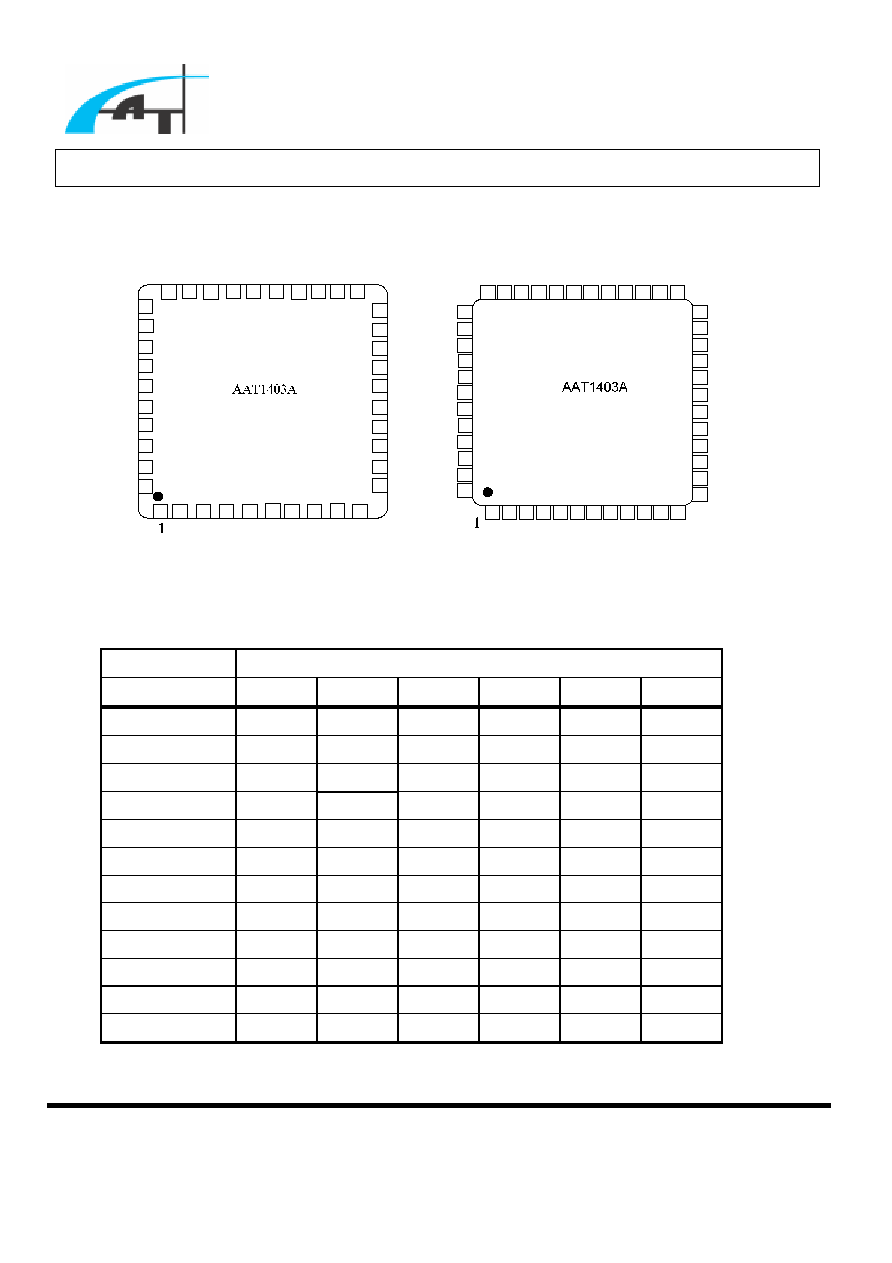
PIN CONFIGURATION
(VQFN-40) (LQFP-48)
FUNCTION TABLE
Condition Channel
Status
-
SD
CH1 CH2 CH3 CH4 CH5 CH6
SD1=
"Lo"
Off
SD1= "Hi"
On
SD2=
"Lo"
Off
SD2=
"Hi"
On
SD3=
"Lo"
Off
SD3=
"Hi"
On
SD4=
"Lo"
Off
SD4=
"Hi"
On
SD5=
"Lo"
Off
SD5=
"Hi"
On
SD6=
"Lo"
Off
SD6= "Hi"
On

Advanced Analog Technology, Inc.
≠
≠
≠
Advanced Analog Technology, Inc
.
≠
Page 3 of 27 V1.0
AAT1403A
PIN DESCRIPTION (VQFN-40)
Pin No
Name
I/O Function
1
SD1
I
ON/OFF Control for Channel 1 (CH1)
2
SD5
I
ON/OFF Control for Channel 5 (CH5)
3
SD6
I
ON/OFF Control for Channel 6 (CH6)
4
IE1
I
Inverted Input for Error Amplifier 1 (EA1)
5
IE5
I
Inverted Input for Error Amplifier 5 (EA5
6
IE6
I
Inverted Input for Error Amplifier 6 (EA6)
7
DTC1
I
Dead Time Control of Channel 1 (CH1)
8
OE1
O
Output for Error Amplifier 1 (EA1)
9
DTC5
I
Dead Time Control of Channel 5 (CH5)
10
OE5
O
Output for Error Amplifier 5 (EA5)
11
DTC6
I
Dead Time Control of Channel 6 (CH6)
12
OE6
O
Output for Error Amplifier 6 (EA6)
13
VB
O
Reference Voltage 2.77V Output
14 GND P
Ground
15
DD
V
P Power
Supply
16
REF
V
O
Reference Voltage 1.26V Output
17
SCP
-
Short Circuit Protect Capacitor Connection Pin
18
SD4
I
ON/OFF Control for Channel 4 (CH4)
19
SD3
I
ON/OFF Control for Channel 3 (CH3)
20
SD2
I
ON/OFF Control for Channel 2 (CH2)
21
IE4A
I
Inverted Input 2 for Error Amplifier 4 (EA4)
22
IE4
I
Inverted Input for Error Amplifier 4 (EA4)
23
IE3
I
Inverted Input for Error Amplifier 3 (EA3)
24
IE2
I
Inverted Input for Error Amplifier 2 (EA2)
25
OE4
O
Output for Error Amplifier 4 (EA4)
26
OE3
O
Output for Error Amplifier 3 (EA3)
27
OE2
O
Output for Error Amplifier 2 (EA2)
28
DTC4
I
Dead Time Control of Channel 4 (CH4)
29
DTC3
I
Dead Time Control of Channel 3 (CH3)
30
DTC2
I
Dead Time Control of Channel 2 (CH2)
31
OUT2
O
CH2 Totem Pole Type Output
32
OUT3
O
CH3 Totem Pole Type Output
33
OUT4
O
CH4 Totem Pole Type Output
34
OUT6_2
O
CH6 Synchronous Rectifier Side Output
35
PVDD
P
Output Buffer Power Supply
36
OUT6_1
O
CH6 Totem Pole Type Output
37
OUT5_1
O
CH5 Totem Pole Type Output
38
OUT5_2
O
CH5 Synchronous Rectifier Side Output
39
OUT1_1
O
CH1 Totem Pole Type Output
40
OUT1_2
O
CH1 Synchronous Rectifier Side Output

Advanced Analog Technology, Inc.
≠
≠
≠
Advanced Analog Technology, Inc
.
≠
Page 4 of 27 V1.0
AAT1403A
PIN DESCRIPTION (LQFP-48)
Pin No
Name
I/O Function
1 NC -
2
SD1
I
ON/OFF Control for Channel 1 (CH1)
3
SD5
I
ON/OFF Control for Channel 5 (CH5)
4
SD6
I
ON/OFF Control for Channel 6 (CH6)
5
IE1
I
Inverted Input for Error Amplifier 1 (EA1)
6
IE5
I
Inverted Input for Error Amplifier 5 (EA5)
7
IE6
I
Inverted Input for Error Amplifier 6 (EA6)
8
DTC1
I
Dead Time Control of Channel 1 (CH1)
9
OE1
O
Output for Error Amplifier 1 (EA1)
10
DTC5
I
Dead Time Control of Channel 5 (CH5)
11
OE5
O
Output for Error Amplifier 5 (EA5)
12 NC -
13 NC -
14
DTC6
I
Dead Time Control of Channel 6 (CH6)
15
OE6
O
Output for Error Amplifier 6 (EA6)
16
VB
O
Reference Voltage 2.77V Output
17 GND P
Ground
18
DD
V
P Power
Supply
19
REF
V
O
Reference Voltage 1.26V Output
20
SCP
-
Short Circuit Protect Capacitor Connection Pin
21
SD4
I
ON/OFF Control for Channel 4 (CH4)
22
SD3
I
ON/OFF Control for Channel 3 (CH3)
23
SD2
I
ON/OFF Control for Channel 2 (CH2)
24 NC -
25 NC -
26
IE4A
I
Inverted Input 2 for Error Amplifier 4 (EA4)
27
IE4
I
Inverted Input for Error Amplifier 4 (EA4)
28
IE3
I
Inverted Input for Error Amplifier 3 (EA3)
29
IE2
I
Inverted Input for Error Amplifier 2 (EA2)
30
OE4
O
Output for Error Amplifier 4 (EA4)
31
OE3
O
Output for Error Amplifier 3 (EA3)
32
OE2
O
Output for Error Amplifier 2 (EA2)
33
DTC4
I
Dead Time Control of Channel 4 (CH4)
34
DTC3
I
Dead Time Control of Channel 3 (CH3)
35
DTC2
I
Dead Time Control of Channel 2 (CH2)
36 NC -
37 NC -
38
OUT2
O
CH2 Totem Pole Type Output
39
OUT3
O
CH3 Totem Pole Type Output
40
OUT4
O
CH4 Totem Pole Type Output
41
OUT6_2
O
CH6 Synchronous Rectifier Side Output
42
PVDD
P
Output Buffer Power Supply
43
OUT6_1
O
CH6 Totem Pole Type Output
44
OUT5_1
O
CH5 Totem Pole Type Output
45
OUT5_2
O
CH5 Synchronous Rectifier Side Output
46
OUT1_1
O
CH1 Totem Pole Type Output
47
OUT1_2
O
CH1 Synchronous Rectifier Side Output
48 NC -

Advanced Analog Technology, Inc.
≠
≠
≠
Advanced Analog Technology, Inc
.
≠
Page 5 of 27 V1.0
AAT1403A
BLOCK DAIGRAM
C H 1
S y n c h r o n o u s
B u c k
C H 2
B o o s t
C H 3
I n v e r t i n g
C H 4
B o o s t
I E 1
O E 1
D T C 1
S D 1
D T C 3
S D 3
I E 3
O E 3
D T C 2
S D 2
I E 2
O E 2
D T C 4
S D 4
I E 4
O E 4
O U T 4
O U T 2
O U T 3
O U T 1 _ 1
P V D D
O U T 1 _ 2
o s c
E A 4
1 .2 4 5 V & 0 .3 7 V
S C P 4
S C P 3
S C P 1
S C P 2
1 . 2 4 5 V
1 . 2 4 5 V
0 . 7 8 3 V
E A 1
E A 2
E A 3
V
D D
G N D
S C P
V
R E F
V B
O S C & S C P & U V L O & V
R E F
C H 5
S y n c h r o n o u s
B u c k
D T C 5
S D 5
I E 5
O E 5
O U T 5 _ 2
O U T 5 _ 1
S C P 5
1 . 2 4 5 V
E A 5
I E 4 A
( W L E D )
C H 6
S y n c h r o n o u s
B o o s t
D T C 6
S D 6
I E 6
O E 6
O U T 6 _ 2
O U T 6 _ 1
S C P 6
1 . 2 4 5 V
E A 6