Advanced Analog Technology, Inc.
≠
≠
≠
Advanced Analog Technology, Inc
.
≠
Page 1 of 10 V 1.0
AAT7205
Details are subject to change without notice.
8+1-CHANNEL BUFFER FOR TFT LCD
FEATURES
8 Channels with Output Current:
mA
30
±
(MAX)
1
com
V
with Output Current:
mA
100
±
(MAX)
Unity Gain Buffer Capable of Driving
Large Capacitive Loads
Input Range Matched to LCD Reference
Requirements
Specified for
20
-
o
C to +85
o
C...6.5V to
16V
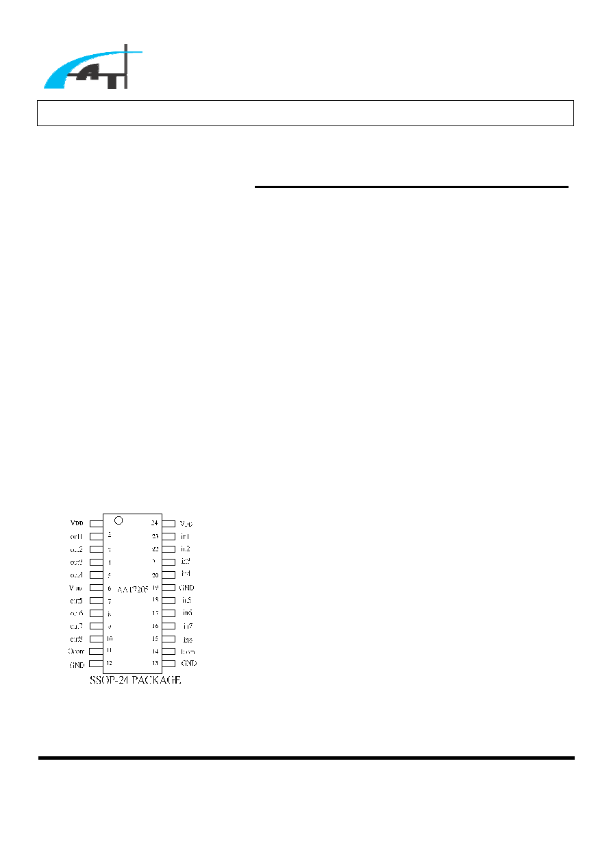
SSOP-24 Package
GENERAL DESCRIPTION
The AAT7205 is specially designed for thin
film transistor liquid crystal display (TFT
LCD). It is a buffer with 8+1 channels which
delivers output current up to 30mA. This
device is equipped with a
com
V
buffer circuit,
two rail-to-rail buffer amplifier circuits, and 6
buffer amplifiers circuits. Each buffer is
capable of driving heavy capacitive loads and
offers fast load current (
com
V
: 100mA, the
others: 30mA).
PIN CONFIGURATION
TOP VIEW
Advanced Analog Technology, Inc.
≠
≠
≠
Advanced Analog Technology, Inc
.
≠
Page 2 of 10 V 1.0
AAT7205
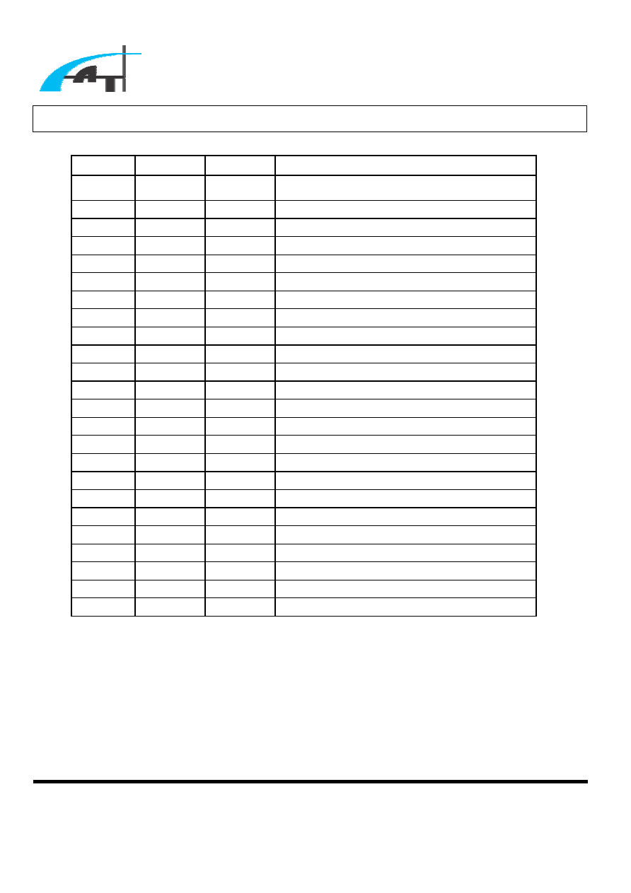
PIN DESCRIPTION
PIN NO.
NAME
I/O
DESCRIPTION
1
DD
V
I
Power Supply
2 out1 O
Buffer
Channel
1 Output
3 out2 O
Buffer
Channel
2 Output
4 out3 O
Buffer
Channel
3 Output
5
out4
O
Buffer Channel 4 Output
6
DD
V
I Power
Supply
7
out5
O
Buffer Channel 5 Output
8
out6
O
Buffer Channel 6 Output
9
out7
O
Buffer Channel 7 Output
10
out8
O
Buffer Channel 8 Output
11
com
O
O
Com Buffer Output
12 GND I
Ground
13 GND I
Ground
14
com
I
I
Com Buffer Input
15
in8
I
Buffer Channel 8 Input
16
in7
I
Buffer Channel 7 Input
17
in6
I
Buffer Channel 6 Input
18
in5
I
Buffer Channel 5 Input
19 GND I
Ground
20
in4
I
Buffer Channel 4 Input
21
in3
I
Buffer Channel 3 Input
22
in2
I
Buffer Channel 2 Input
23
in1
I
Buffer Channel 1 Input
24
DD
V
I Power
Supply

Advanced Analog Technology, Inc.
≠
≠
≠
Advanced Analog Technology, Inc
.
≠
Page 3 of 10 V 1.0
AAT7205
ABSOLUTE MAXIMUM RATINGS
CHARACTERISTICS SYMBOL VALUE UNIT
Supply Voltage
DD
V
+18 V
Input Voltage
I
V
5
.
0
-
to
5
.
0
V
DD
+
V
Output Voltage
O
V
5
.
0
-
to
5
.
0
V
DD
+
V
Output Loading Current for Gamma
Rail-to-Rail Buffer
30
±
mA
Output Loading Current for Com Buffer
L
I
100
±
mA
Maximum Junction Temperature
T
J
+125
o
C
Operating Temperature
C
T
20
-
to +85
o
C
Storage Temperature
storage
T
45
-
to +125
o
C
Lead Temperature (Soldering for 10
Seconds)
---
260
o
C
Note1: Values beyond absolute maximum ratings may cause permanent damage to the device.

Advanced Analog Technology, Inc.
≠
≠
≠
Advanced Analog Technology, Inc
.
≠
Page 4 of 10 V 1.0
AAT7205
ELECTRICAL CHARACTTERISTICS
(V
DD
=10V, T
C
=25
o
C UNLESS
OTHERWISE SPECIFIED)
POWER SUPPLY PERFORMANCE
PARAMETER
TEST
CONDITIONS
MN
TYP
MAX
UNITS
Power Supply Rejection
Ratio
PSRR
DD
V
is Moved from 6.5V
to 15.5V
80 dB
Supply Current
S
I
7.4
mA
INPUT CHARACTERISTICS
PARAMETER
TEST
CONDITIONS
MIN
TYP
MAX
UNITS
Input Offset Voltage
OS
V
I
V =
DD
V
/2,
O
V =
DD
V
/2
2 12 mV
Input Bias Current
B
I
I
V =
DD
V
/2,
O
V =
DD
V
/2
2 50 nA

Advanced Analog Technology, Inc.
≠
≠
≠
Advanced Analog Technology, Inc
.
≠
Page 5 of 10 V 1.0
AAT7205
ELECTRICAL CHARACTTERISTICS (V
DD
=10V, T
C
=25
o
C UNLESS
OTHERWISE SPECIFIED) (CONT.)
OUTPUT CHARACTERISTICS
PARAMETER
TEST
CONDITIONS
MIN
TYP
MAX
UNITS
L
I =5mA(Buffer 1,8)
I
V =0V
0.08 0.15 V
Output Swing Low
OL
V
L
I =10mA
(Buffer 2,3,4,5,6,7)
I
V =1V
1.02
1.05 V
L
I =
5
-
mA
(Buffer 1,8)
I
V =10V
9.85
9.92 V
Output Swing High
OH
V
L
I =
10
-
mA
(Buffer 2,3,4,5,6,7)
I
V =9V
8.95
8.98 V
OL
V
L
I =10mA
I
V =5V
5.02
5.04 V
Output Swing
(Buffer 2,3,4,5,6,7)
OH
V
L
I =
10
-
mA
I
V =5V
4.96
4.98 V
OL
V
L
I =50mA
I
V =5V
5.03
5.05 V
Output Swing (COM)
OH
V
I
L
=
50
-
mA
I
V =5V
4.95
4.97 V
(Buffer 2~7 )
70
±
mA
Short Circuit Current
I
SC
(Com Buffer, Buffer1,8)
180
±
mA
AC Characteristics
Parameter
Test
Conditions
Min
Typ Max Units
Slew Rate [Note 2]
SR
I
V =2V to 8V, 20% to 80%
1 V/
s
µ
Settling Time
s
t
I
V =4.5V to 5.5V 0.1%
I
V =5.5V to 4.5V 0.1%
5
s
µ
Note 2: Slew rate is measured on rising and falling edges.