 | –≠–ª–µ–∫—Ç—Ä–æ–Ω–Ω—ã–π –∫–æ–º–ø–æ–Ω–µ–Ω—Ç: AAT8636 | –°–∫–∞—á–∞—Ç—å:  PDF PDF  ZIP ZIP |
Advanced Analog Technology, Inc.
≠
≠
≠
Advanced Analog Technology, Inc
.
≠
Page 1 of 16 V 1.0
AAT8636 Series
Details are subject to change without notice
ONE-CELL LI-ION BATTERY PROTECTION IC
FEATURES
∑
Ideal for One-Cell Rechargeable Li-Ion Battery
Pack.
∑
Low Current Consumption
A
0
.
3
µ
..............Supply Current (Typical)
A
1
.
0
µ
..............Standby Current
∑
High Withstand Voltage
Absolute Maximum Ratings..22V (
VN
V
DD
-
)
∑
High Accuracy Voltage Detection
Over Charge Detector...............
mV
20
±
Over Discharge Detector..........
%
5
.
2
±
∑
Over Current and Short Circuit Protection
∑
Wide Operating Temperature Range
C
40
o
-
to
C
85
o
∑
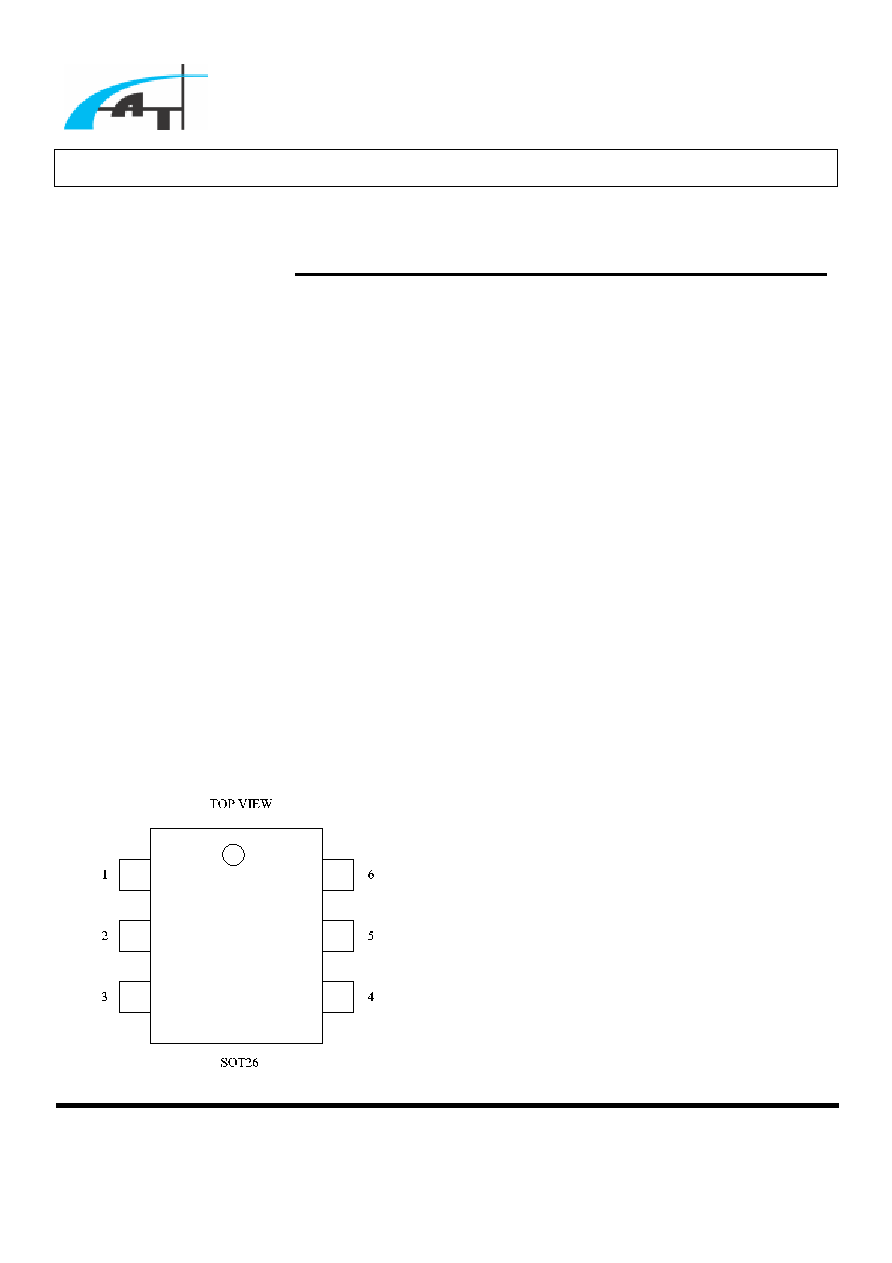
Ultra Small Package........SOT26
PIN CONFIGURATION
OUT
D
VN
OUT
C
GND
ext
C
DD
V
GENERAL DESCRIPTION
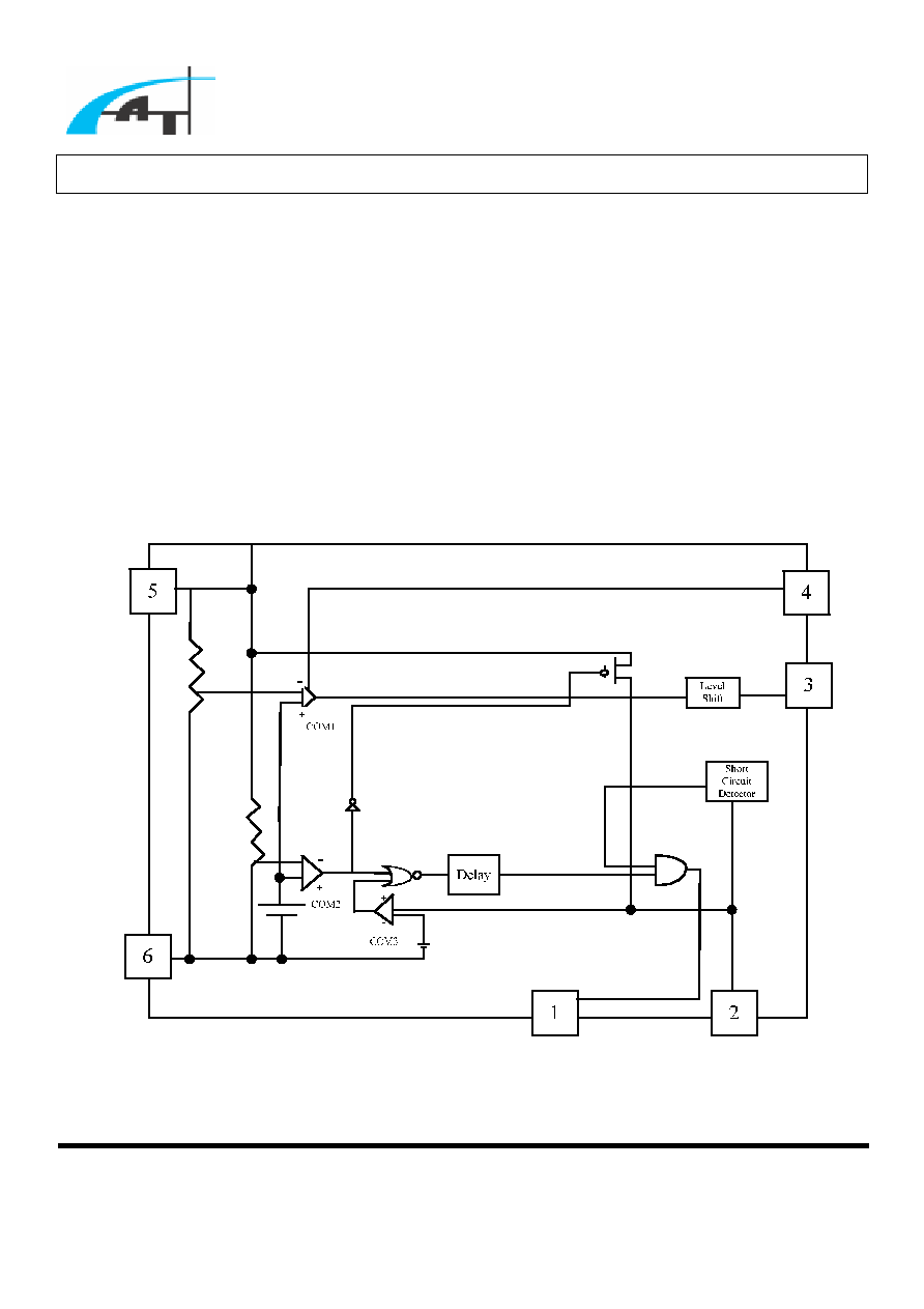
The AAT8636 series are protection ICs designed
to safeguard one-cell rechargeable Li-Ion battery
pack against over charge, over discharge, over
current, and short circuit. The AAT8636 series
use advanced high voltage CMOS process to
provide high accuracy voltage detection and low
current consumption.
The AAT8636 series incorporate a reference unit
and three voltage detectors. During the charging
process, when the cell voltage (
DD
V ) is charged to
a value higher than the over charge threshold
voltage (
1
C
V ), the over charge detector (COM1)
will switch the output pin (
OUT
C
) to a low level
within a delay time (
1
C
t ), and thus turning off the
MOSFET connected to the charging path. The
OUT
C
pin may change to high level again when
the
DD
V
voltage falls below "
HYS
1
C
V
V
-
", or
when
DD
V falls below
1
C
V while the charger is
disconnected from the battery pack.
During the discharging process, when the
DD
V
drops to a value lower than the over-discharge
threshold voltage (
1
D
V
), the over-discharge
detector (COM2) will switch
OUT
D
to low level
within a delay time (
1
D
t ), and thus turning off the
MOSFET connecting to the discharging path. In
the mean time, the AAT8636 series will enter a
low current standby mode. Once into standby
mode, the systems can only be released from
Advanced Analog Technology, Inc.
≠
≠
≠
Advanced Analog Technology, Inc
.
≠
Page 2 of 16 V 1.0
AAT8636 Series
standby mode right after the battery pack is
connected to a charger.
The conditions of over current and short circuit
protection are both determined by the voltage at
the VN pin. As the voltage of VN pin reaches a
value higher than
OC
V
, which indicates an
undesirable large current is flowing through the
path,
OUT
D
will be switched to low and the path
is cut-off right after an internally pre-set delay
time (
OC
t
) elapses. In the case of short circuit, i.e.
VN rises above
short
V
, the path will also be cut-off
but with almost no delay time. Once the over
current or factors contributing to short circuit is
removed, the built-in resistor at the VN pin,
typically 100
k
, will pull VN down to GND and
bring the IC back to standard operation.
Together with the application circuit, the
AAT8636 series will function as a consummate
protector, which promotes safe usage and the
sustainability of Li-Ion battery packs.
BLOCK DIAGRAM
GND
DD
V
OUT
C
OUT
D
VN
ext
C

Advanced Analog Technology, Inc.
≠
≠
≠
Advanced Analog Technology, Inc
.
≠
Page 3 of 16 V 1.0
AAT8636 Series
PIN DESCRIPTION
Pin No.
Symbol
Description
1
OUT
D
Output of Over-Discharge Detection
2
VN
Pin for Charger Negative Input
3
OUT
C
Output of Over-Charge Detection
4
ext
C
Pin for External Capacitor Setting COM1 Delay Time
5
DD
V
Power Supply
6 GND
Ground
TYPICAL APPLICATION
DD
V
GND
VN
ext
C
OUT
D
OUT
C
1
C
3
C
2
C
F
1
.
0
µ
F
1
.
0
µ
F
01
.
0
µ
1
R
2
R
100
k
1
+
-
Advanced Analog Technology, Inc.
≠
≠
≠
Advanced Analog Technology, Inc
.
≠
Page 4 of 16 V 1.0
AAT8636 Series
ABSOLUTE MAXIMUM RATINGS
Symbol Item
Rating Unit
DD
V
Supply Voltage
3
.
0
-
to 12
V
VN VN
Pin
22
V
DD
-
to
DD
V +0.3
V
Cext
V
Input Voltage
ext
C
Pin
GND
3
.
0
-
to V
DD
+0.3
V
Cout
V
OUT
C
Pin
22
V
DD
-
to
DD
V +0.3
V
Dout
V
Output Voltage
OUT
D
Pin
GND
3
.
0
-
to
DD
V +0.3
V
d
P
Power Dissipation
160
mW
C
T
Operating Temperature Range
40
-
to +85
storage
T
,
j
T
Storage and Junction Temperature
50
-
to +120
ABSOLUTE MAXIMUM RATINGS
Stresses beyond those listed under "Absolute Maximum Ratings" may cause permanent damage to the
device. Exposure to absolute maximum rating conditions for extended period of time may affect device
reliability.

Advanced Analog Technology, Inc.
≠
≠
≠
Advanced Analog Technology, Inc
.
≠
Page 5 of 16 V 1.0
AAT8636 Series
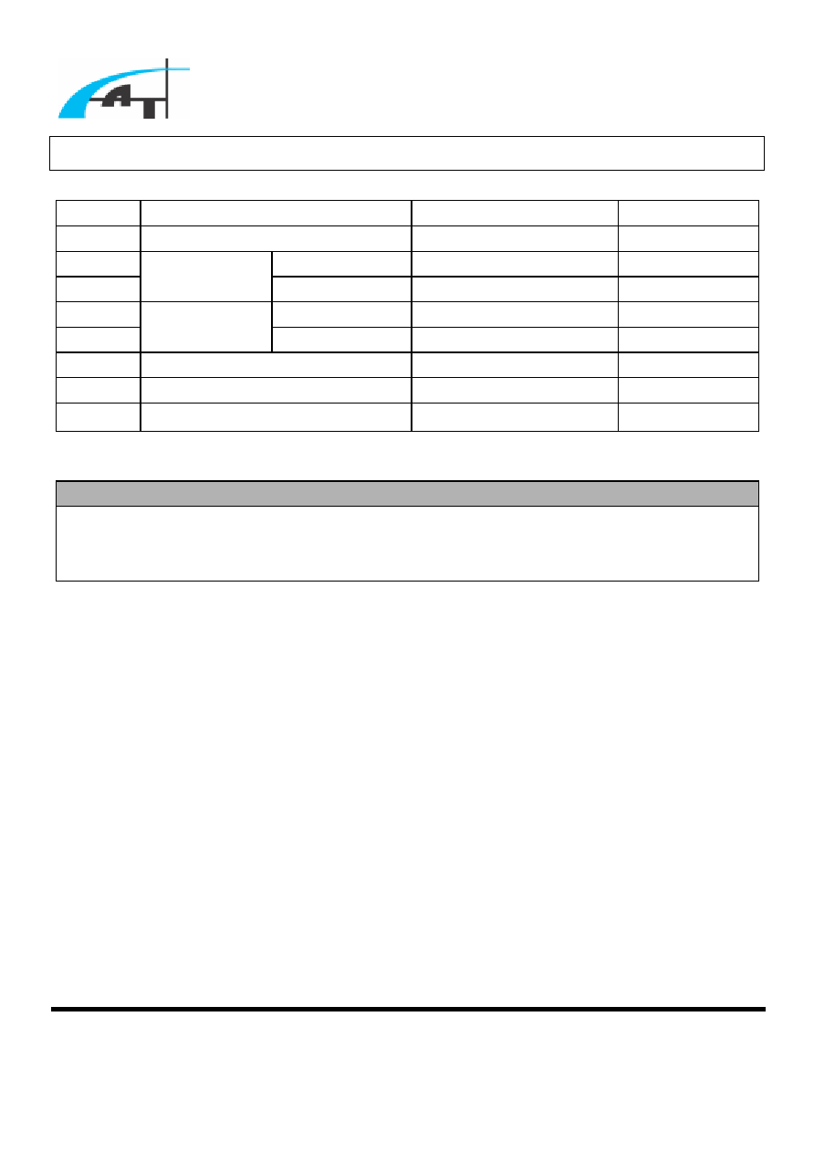
ELECTRICAL CHARACTERISTICS
∑AAT8636A
oper
T
=25
Symbol Item
Conditions
Min
Typ
Max
Unit
1
DD
V
Operating Input Voltage
Voltage Defined as
GND
V
DD
-
1.5 10.0
V
1
C
V Over Charge Threshold Voltage
Detect Rising Edge of Supply
Voltage
4.33 4.35 4.37 V
HYS
V
Over Charge Threshold
Hysteresis Range
0.15 0.20 0.25 V
1
C
t Over Charge Delay Time
F
01
.
0
C
3
µ
=
,
DD
V =3.6V to
4.4V
60 75 90
ms
1
D
V
Over Discharge Threshold
Voltage
Detect Falling Edge of
Supply Voltage
2.437 2.500 2.563 V
1
D
t Over Discharge Delay Time
DD
V =3.6V to 2.4V
7 10 13
ms
OC
V Over Current Detection
Voltage
Detect Rising Edge of VN
Pin Voltage
0.17 0.20 0.23 V
OC
t
Over Current Detection Delay
Time
DD
V =3.0V
9 13 17
ms
short
V
Short Circuit Detection Voltage
DD
V =3.0V 2
.
1
V
DD
-
9
.
0
V
DD
-
6
.
0
V
DD
-
V
short
t
Short Circuit Detection Delay
Time
DD
V =3.0V
5 50
s
µ
short
R
Reset Resistance for Over
Current Protection
DD
V =3.6V, VN=1.0V
50 100 150
k
1
OL
V
Nch ON Voltage of
OUT
C
OL
I =50
A
µ
,
DD
V =4.4V
0.35
0.50
V
1
OH
V
Pch ON Voltage of
OUT
C
OH
I
=
50
-
A
µ
,
DD
V =3.9V
3.4 3.7 V
2
OL
V
Nch ON Voltage of
OUT
D
OL
I =50
A
µ
,
DD
V =2.4V
0.2
0.5
V
2
OH
V
Pch ON Voltage of
OUT
D
OH
I
=
50
-
A
µ
,
DD
V =3.9V
3.4 3.7 V
DD
I
Supply Current
DD
V =3.9V,VN =0V
3.0
5.0
A
µ
dby
tan
s
I
Standby Current
DD
V =2.0V
0.1
A
µ