 | –≠–ª–µ–∫—Ç—Ä–æ–Ω–Ω—ã–π –∫–æ–º–ø–æ–Ω–µ–Ω—Ç: AZ3842 | –°–∫–∞—á–∞—Ç—å:  PDF PDF  ZIP ZIP |
CURRENT MODE PWM CONTROLLER AZ3842/3/4/5
Advanced Analog Circuits
Data Sheet
1
March 2003
Rev: 1.0
General Description
The AZ3842/3/4/5 are high performance fixed fre-
quency current-mode PWM controller series.
These integrated circuits are optimized for off-line and
DC-DC converter applications with minimum external
components. They feature under-voltage lockout
(UVLO) circuit for low start-up current, trimmed
oscillator for precise duty cycle control, current sense
comparator providing maximum current limiting and a
totem pole output stage for increasing output current.
In addition, these ICs also feature accurate protection
against over-temperature, over-current and maximal
output power.
The AZ3842 and AZ3844 have UVLO thresholds of
15.5V(on) and 10V(off); The corresponding thresholds
for AZ3843 and AZ3845 are 8.4 V(on) and 7.8V(off).
The AZ3842 and AZ3843 can operate approaching
100% duty cycle; AZ3844 and AZ3845 can operate
from zero to 50% duty cycle.
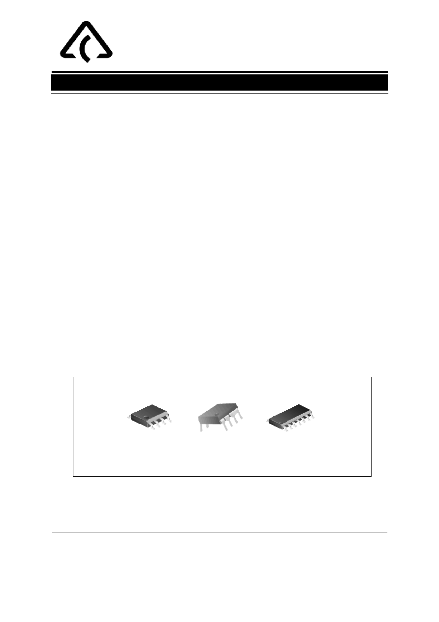
These ICs are available in 3 packages: SOIC-8, DIP-8
and SOIC-14.
Features
∑
Robust V
REF
Line/Load Regulation
Low Line Regulation : 4mV
Low Load Regulation : 4mV
∑
High Stability of Reference Voltage over a Full
Temperature Range: 0.2mV/
o
C
∑
Operating Frequency up to 500KHz
∑
High PWM Frequency Stability over a Full Tem-
perature Range: 2.5%
∑
High PWM Frequency Stability under a Full Sup-
ply Voltage Range: 0.2%
∑
Accurate Over-temperature Protection with Hys-
teresis
∑
UVLO with Hysteresis
Applications
∑
Off-line Converter
∑
DC-DC Converter
∑
Voltage Adapter
∑
CRT Monitor Power Supply
∑
Desktop Power Supply
∑
DVD/STB Power Supply
SOIC-8
DIP-8
SOIC-14
Figure 1. Package Types of AZ3842/3/4/5

CURRENT MODE PWM CONTROLLER AZ3842/3/4/5
Advanced Analog Circuits
Data Sheet
2
March 2003
Rev: 1.0
Figure 2. Pin Configuration of AZ3842/3/4/5 (Top View)
P/M Package
(DIP-8/SOIC-8)
(SOIC-14)
Pin Configuration
COMP
I
SENSE
V
FB
R
T
/C
T
8 V
REF
7 V
CC
6 OUTPUT
5 GND
1
2
3
4
N/C
V
FB
N/C
I
SENSE
N/C
R
T
/C
T
COMP
14 V
REF
13 N/C
12 V
CC
11 PWR V
C
10 OUTPUT
9 GND
8 PWR GND
1
2
3
4
5
6
7
Pin Description
Pin Number
Pin Name
Function
8-pin
14-pin
1
1
COMP
This pin is the Error Amplifier output and is made available for loop compensation.
2
3
V
FB
The inverting input of the Error Amplifier. It is normally connected to the switching
power supply output through a resistor divider.
3
5
I
SENSE
A voltage proportional to inductor current is connected to this input. The PWM uses
this information to terminate the output switch conduction.
4
7
R
T
/C
T
The Oscillator frequency and maximum Output duty cycle are programmed by con-
necting resistor R
T
to V
REF
and capacitor C
T
to ground. Operation to 500 kHz is pos-
sible.
5
GND
The combined control circuitry and power ground.
6
10
OUTPUT
This output directly drives the gate of a power MOSFET. Peak currents up to 1.0 A
are sourced and sunk by this pin.
7
12
V
CC
The positive supply of the control IC.
8
14
V
REF
This is the reference output. It provides charging current for capacitor C
T
through
resistor R
T
.
8
PWR GND
This pin is a separate power ground return that is connected back to the power source.
It is used to reduce the effects of switching transient noise on the control circuitry.
11
PWR V
C
The Output high state (V
OH
) is set by the voltage applied to this pin. With a separate
power source connection, it can reduce the effects of switching transient noise on the
control circuitry.
9
GND
This pin is the control circuitry ground return and is connected back to the power
source ground.
2,4,6,13
N/C
No connection. These pins are not internally connected.
M Package

CURRENT MODE PWM CONTROLLER AZ3842/3/4/5
Advanced Analog Circuits
Data Sheet
3
March 2003
Rev: 1.0
Functional Block Diagram
Figure 3. Functional Block Diagram of AZ3842/3/4/5
V
CC
GND
R
T
/C
T
V
FB
I
SENSE
COMP
V
CC
(PWR V
C
)
V
REF
OUTPUT
A(B)
OSC
VREF
GOOD
LOGIC
OVER TEMP
PROTECT
T
INTERNAL
BIAS
2R
R
S/R
5V
REF
UVLO
2.50V
PWN
LATCH
CURRENT
SENSE
COMPARATOR
ERROR
AMP
34V
1V
7(12)
5(9)
4(7)
2(3)
1(1)
3(5)
7(11)
8(14)
6(10)
S
R
Note: Toggle flip-flop used
for 3844/45 only
(Note)
5(8)
GND
(PWR GND)
A for 8-pin
B for 14-pin
Package
Temperature Range
Part Number
Marking ID
Packing Type
SOIC-8
-40
o
C~85
o
C
AZ3842/3/4/5M
3842/3/4/5M
Tape/Reel/Tube
DIP-8
AZ3842/3/4/5P
AZ3842/3/4/5P
Tube
SOIC-14
AZ3842/3/4/5MM
AZ3842/3/4/5MM
Tape/Reel
Ordering Information

CURRENT MODE PWM CONTROLLER AZ3842/3/4/5
Advanced Analog Circuits
Data Sheet
4
March 2003
Rev: 1.0
Parameter
Symbol
Value
Unit
Supply Voltage
Vcc
30
V
Output Current
Io
1
A
Analog Inputs (8-pin: pin2,3, 14-pin: pin3,5)
V(ANA)
-0.3 to 6.3
V
Error Amp Output Sink Current
I
SINK
(E.A)
10
mA
Power Dissipation at T
A
< 25
o
C (DIP-8)
P
D
(Note 3)
1000
mW
Power Dissipation at T
A
<25
o
C (SOIC-8)
P
D
(Note 3)
460
mW
Power Dissipation at T
A
<25
o
C (SOIC-14)
P
D
(Note 3)
725
mW
Storage Temperature Range
T
STG
-65 ~+150
o
C
Lead Temperature (Soldering, 10sec)
T
LEAD
+300
o
C
Note 1:
Stresses greater than those listed under "Absolute Maximum Ratings" may cause permanent damage to the
device. These are stress ratings only, and functional operation of the device at these or any other conditions beyond those indi-
cated under "Recommended Operating Conditions" is not implied. Exposure to "Absolute Maximum Ratings" for extended
periods may affect device reliability.
Note 2: All voltages are with respect to pin 5 and all currents are positive into specified terminal.
Note 3: Board thickness 1.6mm, board dimension 90mm
x
90mm.
Absolute Maximum Ratings (Note 1, 2)
Parameter
Symbol
Min
Max
Unit
Oscillation Frequency
f
500
KHz
Ambient Temperature
T
A
-40
85
o
C
Recommended Operating Conditions
CURRENT MODE PWM CONTROLLER AZ3842/3/4/5
Advanced Analog Circuits
Data Sheet
5
March 2003
Rev: 1.0
Parameter
Symbol
Conditions
Min
Typ
Max
Unit
REFERENCE SECTION
Reference Output Voltage
V
REF
T
J
=25
o
C, I
REF
=1mA
4.90
5.00
5.10
V
Line Regulation
V
REF
12V
V
CC
25V
4
15
mV
Load Regulation
V
REF
1mA
I
REF
20mA
4
15
mV
Short Circuit Output Current
I
SC
T
A
=25
o
C
-100
-180
mA
Temperature Stability
0.2
0.4
mV/
o
C
Output Noise Voltage
(Note 6)
50
µV
Long Term Stability
T
A
=85
o
C, 1000 hours
5
25
mV
OSCILLATOR SECTION
Oscillation Frequency
f
T
J
=25
o
C
47
52
57
KHz
Frequency Change with Voltage
f/f
12V
V
CC
25V
0.2
1
%
Oscillator Amplitude
V
OSC
Pin 4, peak to peak (Note 6)
1.7
V
Temperature Stability
(Note 6)
2.5
%
ERROR AMPLIFIER SECTION
Input Bias Current
I
BIAS
(Note 6)
-0.1
-2
µA
Input Voltage
V
I
Vpin 1=2.5V
2.42
2.50
2.58
V
Open Loop Voltage Gain
A
VOL
2V
V
O
4V
65
90
dB
Power Supply Rejection Ratio
PSRR
12V
V
CC
25V
60
70
dB
Output Sink Current
I
SINK
Vpin2=2.7V, Vpin1=1.1V
2
4
mA
Output Source Current
I
SOURCE
Vpin2=2.3V, Vpin1=5V
-0.5
-0.8
mA
High Output Voltage
V
OH
Vpin2=2.3V, R
L
=15k
to GND
5
6
V
Low Output Voltage
V
OL
Vpin2=2.7V, R
L
=15k
to Pin 8
0.8
1.1
V
CURRENT SENSE SECTION
Gain
GV
(Note 4, 5)
2.85
3
3.15
V/V
Maximum Input Signal
V
I
(MAX)
Vpin1=5V(Note 4)
0.9
1
1.1
V
Power Supply Rejection Ratio
PSRR
12V
V
CC
25V (Note 4, 6)
70
dB
Input Bias Current
I
BIAS
-3
-10
µA
Delay to Output
Vpin3 = 0 to 2V (Note 6)
150
300
ns
OUTPUT SECTION
Low Output Voltage
V
OL
I
SINK
= 20mA
0.1
0.4
V
I
SINK
= 200mA
1.4
2.2
V
High Output Voltage
V
OH
I
SOURCE
= 20mA
13
14
V
I
SOURCE
= 200mA
12
13
V
Rise Time
t
R
T
J
=25
o
C, C
L
=1nF (Note 6)
50
150
ns
(V
CC
=15V, R
T
=10k
C
T
=3.3nF, T
A
= -40
o
C to +85
o
C, unless otherwise specified.)
Electrical Characteristics