ABB Semiconductors AG reserves the right to change specifications without notice.
V
RRM
=
400 V
I
FAVM
=
11350 A
I
FRMS
=
17800 A
I
FSM
=
85000 A
V
F0
=
0.74 V
r
F
=
0.018 m
Doc. No. 5SYA1159-01 Oct.00
∑ Optimized for high current rectifiers
∑ Very low on-state voltage
∑ Very low thermal resistance
Blocking
V
RRM
Repetitive peak reverse voltage
400 V
Half sine wave, t
P
= 10 ms, f = 50 Hz
V
RSM
Maximum peak reverse voltage
450 V
Half sine wave, t
P
= 10 ms
I
RRM
Repetitive peak reverse current
50 mA T
j
= 170 ∞C
V
R
= V
RRM
Mechanical
F
M
Mounting force
min.
35 kN
max.
40 kN
a
Acceleration:
Device unclamped
Device clamped
50
200
m/s
2
m/s
2
m
Weight
0.22 kg
D
S
Surface creepage distance
4 mm
D
a
Air strike distance
4 mm
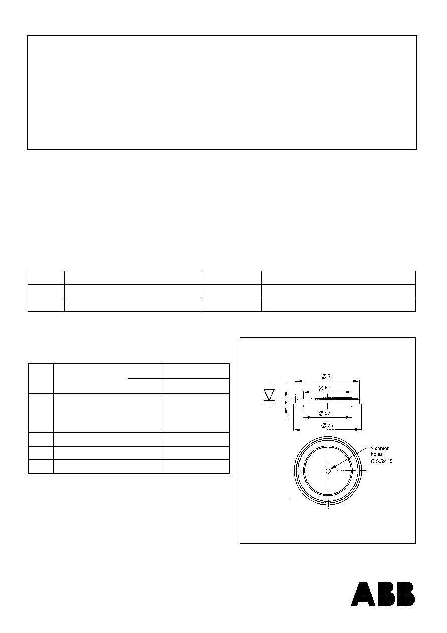
Fig. 1
Outline drawing.
All dimensions are in millimeters and represent
nominal values unless stated otherwise.
Rectifier Diode
5SDD 0120C0400
5SDD 0120C0400
ABB Semiconductors AG reserves the right to change specifications without notice.
page 2 of 4
Doc. No. 5SYA1159-01 Oct.00
On-state
I
FAVM
Max. average on-state current
11350 A
I
FRMS
Max. RMS on-state current
17800 A
Half sine wave, T
c
= 85 ∞C
85000 A
t
p
=
10 ms Before surge
I
FSM
Max. peak non-repetitive surge current
92500 A
t
p
=
8.3 ms T
j
= 170 ∞C
ÚI
2
dt
Max. surge current integral
36100 kA
2
s t
p
=
10 ms After surge:
35700 kA
2
s t
p
=
8.3 ms V
R
0V
V
F min
Minimum on-state voltage
0.83 V
V
F max
Maximum on-state voltage
0.88 V
I
F
=
8000 A
T
j
= 170 ∞C
V
F0
Threshold voltage
0.74 V
Approximation for T
j
= 170 ∞C
r
F
Slope resistance
0.018 m I
F
=
8 - 18 kA
Thermal characteristics
T
j
Operating junction temperature range
-40...170 ∞C
T
stg
Storage temperature range
-40...170 ∞C
12 K/kW Anode side cooled
12 K/kW Cathode side cooled
R
thJC
Thermal resistance
junction to case
6 K/kW Double side cooled
6 K/kW Single side cooled
R
thCH
Thermal resistance
case to heatsink
3 K/kW Double side cooled
F
M
= 35...40 kN
)
e
-
(1
R
=
(t)
Z
4
1
i
/
t
-
thJC
i
Â
=
i
i
1
2
3
4
R
i
(K/kW)
3.37
1.50
0.63
0.67
i
(s)
0.095
0.048
0.0035
0.001
F
M
= 35...40 kN
10
-3
10
-2
10
-1
10
0
t [s]
0
2
4
6
8
Z
thJC
[K/kW]
Double sided cooling
F
m
= 35...40 kN
5
S
DD
0
12
0
C
0
4
0
0
Double side cooled
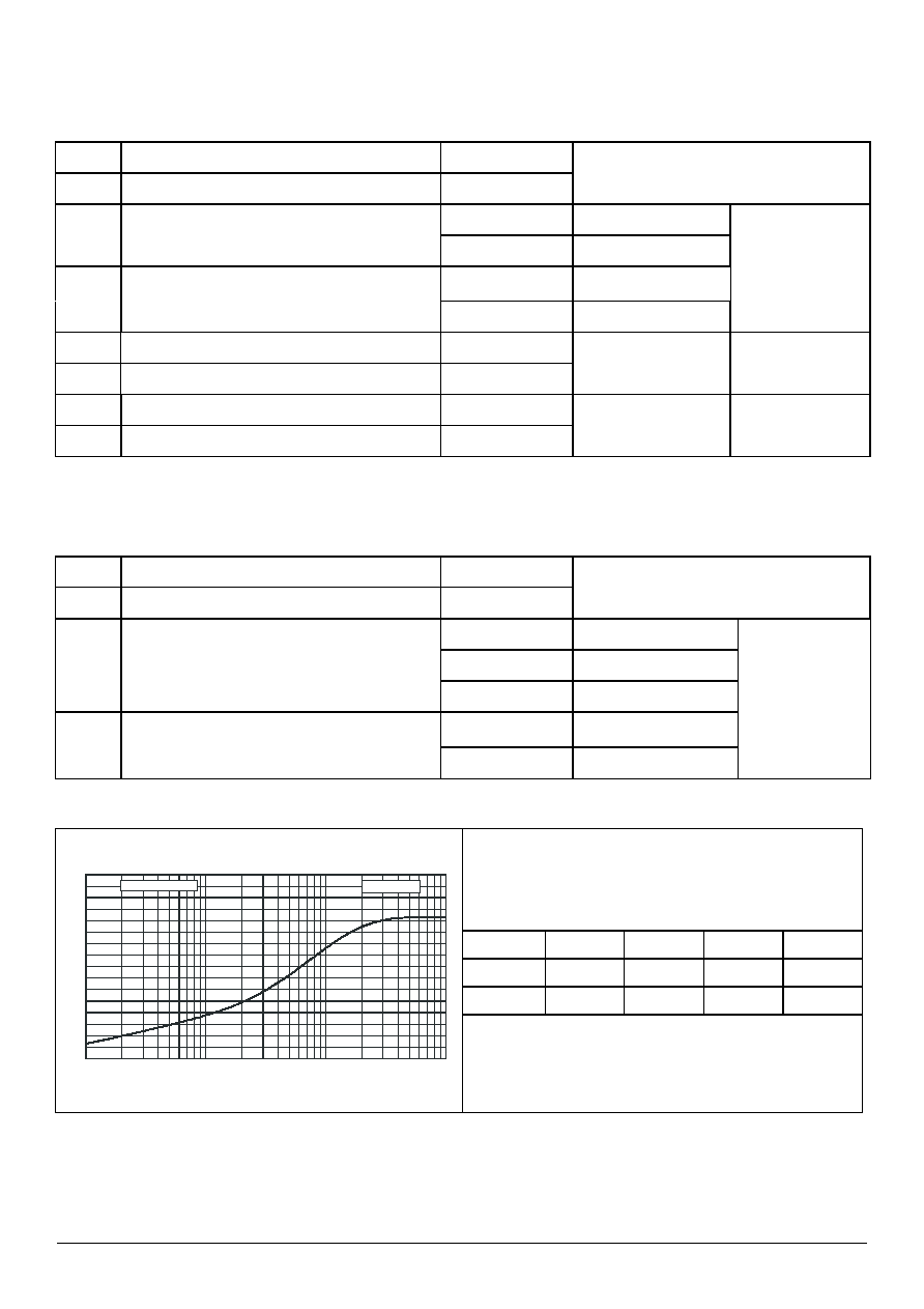
Fig. 2 Transient thermal impedance (junction-to-case) vs. time in analytical and graphical forms.
5SDD 0120C0400
ABB Semiconductors AG reserves the right to change specifications without notice.
page 3 of 4
Doc. No. 5SYA1159-01 Oct.00
On-state characteristics
Surge current characteristics
0.0
0.2
0.4
0.6
0.8
1.0
1.2
1.4
1.6
V
F
[V]
0
2000
4000
6000
8000
10000
12000
14000
16000
18000
I
F
[A]
min.
max.
T
j
= 170∞C
5S
D
D
0
120C
040
0
10
0
10
1
10
2
t [ms]
I
FSM
[kA]
40
60
80
100
120
140
I
FSM
Úi
2
t
Ú i
2
dt [MA
2
s]
24
28
32
36
40
44
T
j
= 170∞C
5SDD 0120C0400
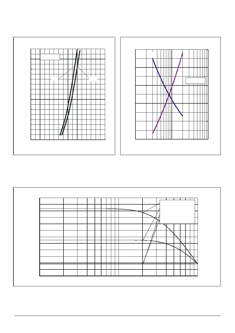
Fig. 3
Forward current vs. forward voltage (min.
and max. values).
Fig. 4 Surge current and fusing integral vs. pulse
width (max. values) for non-repetitive, half-
sinusoidal surge current pulses.
Current load capability
1
10
100
16
18
20
22
24
26
28
n =
50 pulses
n = 100 pulses
n = 500 pulses
n = 1000 pulses
I ( kA )
ID vs. ED, 1000 Hz square wave, T = 100 ∞C
D
C
Duty cycle ED (%)
5S
D
D
012
0C
0400
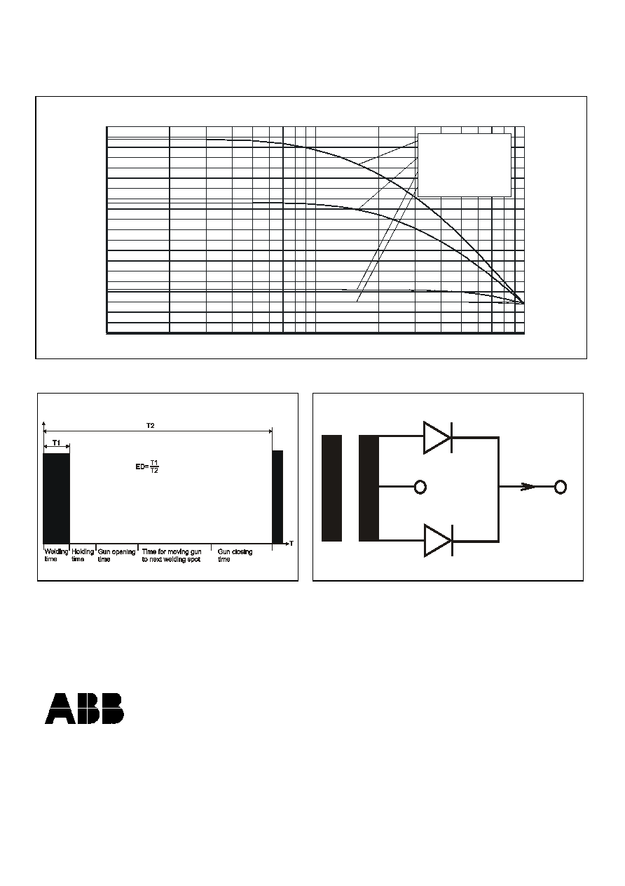
Fig. 5
DC-output current with single-phase centre tap
5SDD 0120C0400
Current load capacity, cont.
1
10
100
16
18
20
22
24
26
28
30
32
34
36
n =
50 pulses
n = 100 pulses
n = 500 pulses
n = 1000 pulses
Duty cycle ED (%)
I
D
( k A )
ID vs. ED, 1000 Hz square-wave, T = 60 ∞C
h
5S
D
D
012
0C
0400
Fig. 6
DC-output current with single-phase centre tap
-
+
I
D
Fig. 7 Definition of ED for typical welding
sequence
Fig. 8 Definition of ID for single-phase centre tap
ABB Semiconductors AG reserves the right to change specifications without notice.
ABB Semiconductors AG
Fabrikstrasse 3
CH-5600 Lenzburg, Switzerland
Telephone +41 (0)62 888 6419
Fax +41 (0)62 888 6306
Email abbsem@ch.abb.com
Internet www.abbsem.com
Doc. No. 5SYA1159-01 Oct.00