
ABB Semiconductors AG reserves the right to change specifications without notice.
V
RRM
=
4500 V
I
FAVM
=
1400 A
I
FSM
=
25 kA
V
F0
=
1.2 V
r
F
=
0.32 m
V
DClink
=
2200 V
Doc. No. 5SYA1110-02 Sep. 01
∑ Patented free-floating silicon technology
∑ Low on-state and switching losses
∑ Optimized for use as freewheeling diode in GTO converters with low DC link
voltages
∑ Standard press-pack housing, hermetically plasma-welded
∑ Cosmic radiation withstand rating
Blocking
V
RRM
Repetitive peak reverse voltage
4500 V
Half sine wave, t
P
= 10 ms, f = 50 Hz
I
RRM
Repetitive peak reverse current
50 mA
V
R
= V
RRM,
T
j
= 125∞C
V
DClink
Permanent DC voltage for 100 FIT
failure rate
2200 V
100% Duty
V
DClink
Permanent DC voltage for 100 FIT
failure rate
V
5% Duty
Ambient cosmic radiation at
sea level in open air.
Mechanical data
(see Fig. 12)
min.
36 kN
F
m
Mounting force
max.
44 kN
a
Acceleration:
Device unclamped
Device clamped
50
200
m/s
2
m/s
2
m
Weight
0.83 kg
D
S
Surface creepage distance
30 mm
D
a
Air strike distance
20 mm
Fast Recovery Diode
5SDF 14H4505
5SDF 14H4505
ABB Semiconductors AG reserves the right to change specifications without notice.
Doc. No. 5SYA1110-02 Sep. 01
page 2 of 6
On-state
(see Fig. 2, 3)
I
FAVM
Max. average on-state current
1400 A
I
FRMS
Max. RMS on-state current
2200 A
Half sine wave, T
c
= 85∞C
I
FSM
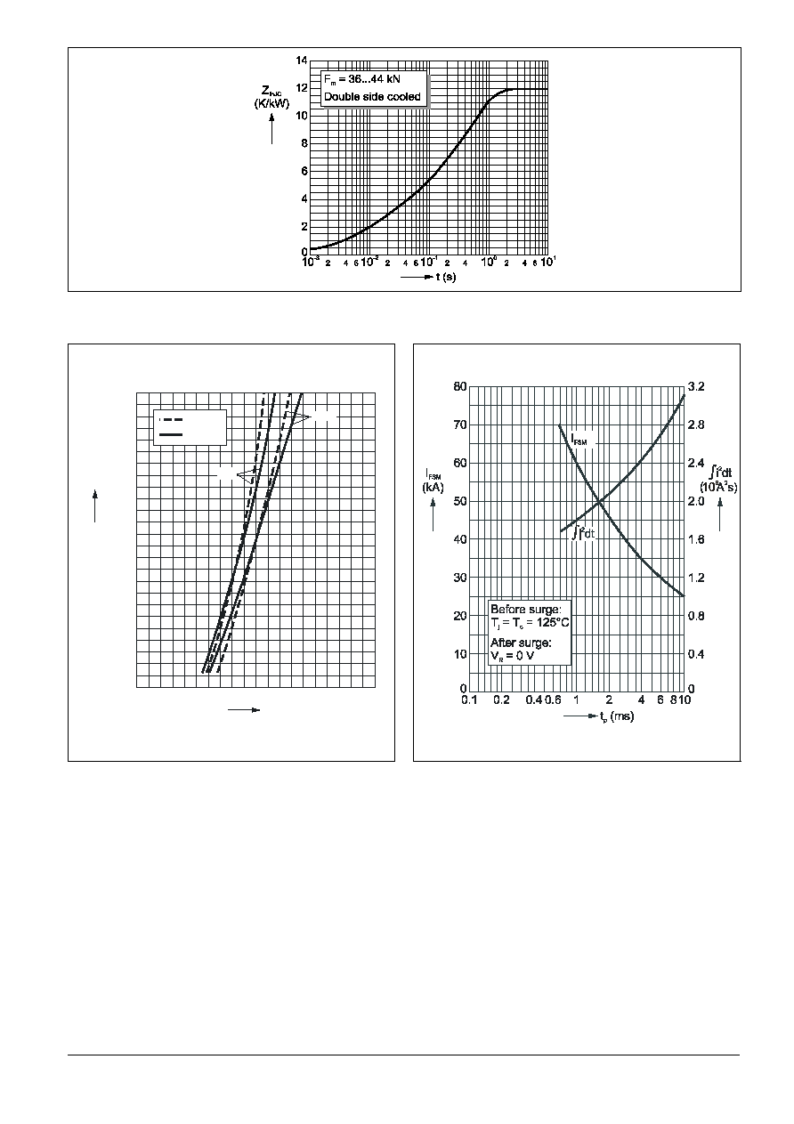
Max. peak non-repetitive
25 kA
tp
=
10 ms
Before surge:
surge current
60 kA
tp =
1 ms
T
c
= T
j
= 125∞C
3.13
10
6
A
2
s
tp =
10 ms
After surge:
ÚI
2
dt
Max. surge current integral
1.8
10
6
A
2
s
tp =
1 ms
V
R
0 V
V
F
Forward voltage drop
2 V
I
F
=
2500 A
V
F0
Threshold voltage
1.2 V
Approximation for
r
F
Slope resistance
0.32 m
I
F
= 400...4000
A
T
j
= 125∞C
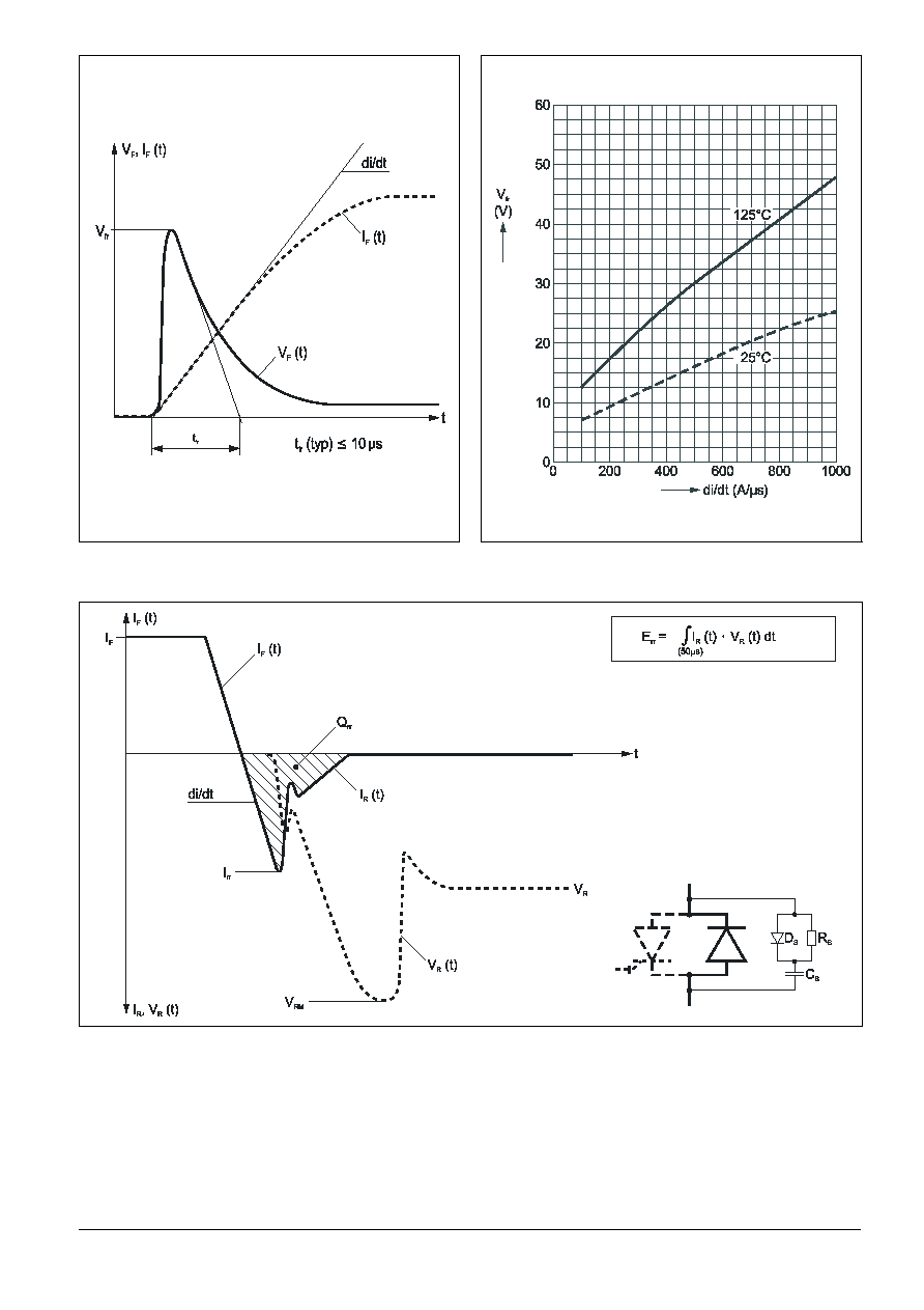
Turn-on
(see Fig. 4, 5)
V
fr
Peak forward recovery voltage
30 V
di/dt = 500 A/µs, T
j
= 125∞C
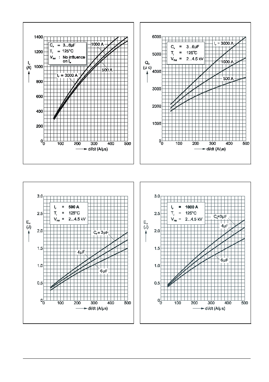
Turn-off
(see Fig. 6 to 11)
I
rr
Reverse recovery current
1000 A
Q
rr
Reverse recovery charge
3700 µC
E
rr
Turn-off energy
1.6 J
di/dt = 300 A/µs,
I
F
= 1000 A,
T
j
= 125∞C,
V
RM
= 4500 V,
C
S
= 3µF (GTO snubber circuit)
Thermal
(see Fig. 01)
T
j
Operating junction temperature range
-40...125∞C
T
stg
Storage temperature range
-40...125∞C
R
thJC
Thermal resistance junction to case
24 K/kW
Anode side cooled
24 K/kW
Cathode side cooled
12 K/kW
Double side cooled
R
thCH
Thermal resistance case to heatsink
6 K/kW
Single side cooled
F
m
=
36... 44 kN
3 K/kW
Double side cooled
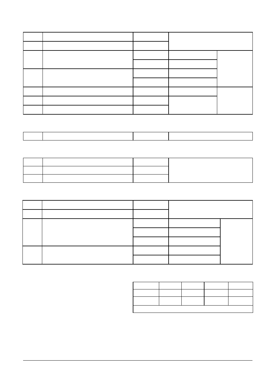
Analytical function for transient thermal impedance.
i
1
2
3
4
R
i
(K/kW)
7.44
2.00
1.84
0.71
i
(s)
0.47
0.091
0.011
0.0047
)
e
-
(1
R
=
(t)
Z
n
1
i
/
t
-
i
thJC
Â
=
i
F
m
= 36... 44 kN Double side cooled
5SDF 14H4505
ABB Semiconductors AG reserves the right to change specifications without notice.
Doc. No. 5SYA1110-02 Sep. 01
page 3 of 6
Fig. 1
Outline drawing. All dimensions are in millimeters and represent nominal values unless stated otherwise.
5000
4000
3000
2000
1000
0
0
1
2
V (V)
F
3
4
I
F
(A)
25∞C
125∞C
max.
typ.
Fig. 2
Forward current vs. forward voltage (typ.
and max. values) and linear approximation
of max. curve at 125∞C.
Fig. 3
Surge current and fusing integral vs. pulse
width (max. values) for non-repetitive, half-
sinusoidal surge current pulses.
5SDF 14H4505
ABB Semiconductors AG reserves the right to change specifications without notice.
Doc. No. 5SYA1110-02 Sep. 01
page 4 of 6
Fig. 4
Typical forward voltage waveform when the
diode is turned on with a high di/dt.
Fig. 5
Forward recovery voltage vs. turn-on di/dt
(max. values).
Fig. 6
Typical current and voltage waveforms at turn-off when the diode is connected to an RCD snubber, as
often used in GTO circuits.
5SDF 14H4505
ABB Semiconductors AG reserves the right to change specifications without notice.
Doc. No. 5SYA1110-02 Sep. 01
page 5 of 6
Fig. 7
Reverse recovery current vs. turn off di/dt
(max. values).
Fig. 8
Reverse recovery charge vs. turn off di/dt
(max. values).
Fig. 9
Turn-off energy vs. turn-off di/dt for I
F
= 500
A (max. values).
Fig. 10 Turn-off energy vs. turn-off di/dt for I
F
= 1000
A (max. values).