
ABB Semiconductors AG reserves the right to change specifications without notice.
V
DRM
=
2500 V
I
TGQM
=
1500 A
I
TSM
=
10 kA
V
T0
=
1.55 V
r
T
=
0.63 m
V
DClin
=
1400 V
Gate turn-off Thyristor
5SGA 15F2502
Doc. No. 5SYA 1214-01 Aug. 2000
∑
Patented free-floating silicon technology
∑
Low on-state and switching losses
∑
Annular gate electrode
∑
Industry standard housing
∑
Cosmic radiation withstand rating
Blocking
V
DRM
Repetitive peak off-state voltage
2500
V
V
GR
2V
V
RRM
Repetitive peak reverse voltage
17
V
I
DRM
Repetitive peak off-state current
100
mA
V
D
= V
DRM
V
GR
2V
I
RRM
Repetitive peak reverse current
50
mA
V
R
= V
RRM
R
GK
=
V
DClink
Permanent DC voltage for 100
FIT failure rate
1400
V
0
T
j
125 ∞C. Ambient cosmic radiation
at sea level in open air.
Mechanical data
(see Fig. 19)
min.
14 kN
F
m
Mounting force
max.
16 kN
A
Acceleration:
Device unclamped
Device clamped
50
200
m/s
2
m/s
2
M
Weight
0.6 kg
D
S
Surface creepage distance
25 mm
D
a
Air strike distance
15 mm

5SGA 15F2502
ABB Semiconductors AG reserves the right to change specifications without notice.
Doc. No. 5SYA 1214-01 Aug. 2000
page 2 of 9
GTO Data
On-state
I
TAVM
Max. average on-state current
550 A
Half sine wave, T
C
= 85 ∞C
I
TRMS
Max. RMS on-state current
870 A
I
TSM
10 kA
t
P
=
10 ms
T
j
=
125∞C
Max. peak non-repetitive
surge current
20 kA
t
P
=
1 ms
After surge:
I
2
t
Limiting load integral
0.50
10
6
A
2
s
t
P
=
10 ms
V
D
= V
R
= 0V
0.20
10
6
A
2
s
t
P
=
1 ms
V
T
On-state voltage
2.50 V
I
T
=
1500 A
V
T0
Threshold voltage
1.55 V
I
T
=
300 - 2000 A
T
j
=
125 ∞C
r
T
Slope resistance
0.63 m
I
H
Holding current
50 A
T
j
= 25 ∞C
Gate
V
GT
Gate trigger voltage
1.5
V
V
D
= 24 V
T
j
=
25 ∞C
I
GT
Gate trigger current
1.5
A
R
A
= 0.1
V
GRM
Repetitive peak reverse voltage
17
V
I
GRM
Repetitive peak reverse current
20
mA
V
GR
= V
GRM
Turn-on switching
di/dt
crit
Max. rate of rise of on-state
400 A/µs
f = 200Hz
I
T
= 1500 A,
T
j
= 125 ∞C
current
600 A/µs
f = 1Hz
I
GM
= 30 A, di
G
/dt = 20 A/µs
t
d
Delay time
2.0 µs
V
D
=
0.5 V
DRM
T
j
=
125 ∞C
t
r
Rise time
4.0 µs
I
T
=
1500 A
di/dt =
200 A/µs
t
on(min)
Min. on-time
80 µs
I
GM
=
30 A
di
G
/dt =
20 A/µs
E
on
Turn-on energy per pulse
0.50 Ws
C
S
=
3 µF
R
S
=
5
Turn-off switching
1500 A
V
DM
= V
DRM
di
GQ
/dt =
30 A/µs
I
TGQM
Max controllable turn-off
current
C
S
= 3 µF
L
S
0.3 µH
t
s
Storage time
15.0 µs
V
D
= Ω V
DRM
V
DM
=
V
DRM
t
f
Fall time
2.0 µs
T
j
=
125 ∞C di
GQ
/dt =
30 A/µs
t
off(min)
Min. off-time
80 µs
I
TGQ
= I
TGQM
E
off
Turn-off energy per pulse
2.0 Ws
C
S
=
3 µF R
S
=
5
I
GQM
Peak turn-off gate current
450 A
L
S
0.3 µH
5SGA 15F2502
ABB Semiconductors AG reserves the right to change specifications without notice.
Doc. No. 5SYA 1214-01 Aug. 2000
page 3 of 9
Thermal
T
j
Storage and operating
0...125∞C
junction temperature range
R
thJC
Thermal resistance
49
K/kW
Anode side cooled
junction to case
60
K/kW
Cathode side cooled
27
K/kW
Double side cooled
R
thCH
Thermal resistance case to
16
K/kW
Single side cooled
heat sink
8
K/kW
Double side cooled
i
1
2
3
4
R
I
(K/kW)
15
5.2
7.5
0.1
Analytical function for transient thermal
impedance:
)
e
-
(1
R
=
(t)
Z
4
1
i
/
t
-
thJC
i
=
i
i
(s)
0.461
0.095
0.012
0.001
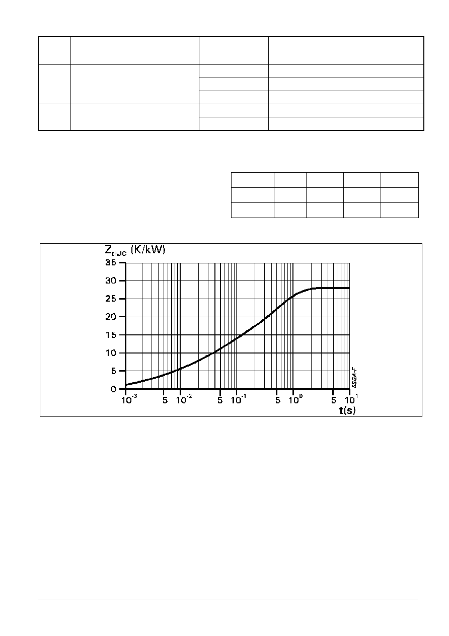
Fig. 1
Transient thermal impedance, junction to case.
5SGA 15F2502
ABB Semiconductors AG reserves the right to change specifications without notice.
Doc. No. 5SYA 1214-01 Aug. 2000
page 4 of 9
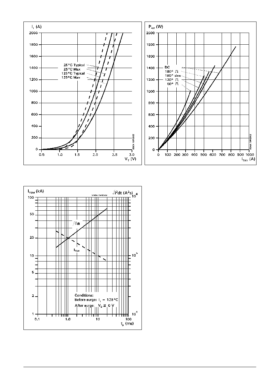
Fig. 2
On-state characteristics
Fig. 3
Average on-state power dissipation vs.
average on-state current.
Fig. 4
Surge current and fusing integral vs. pulse
width
5SGA 15F2502
ABB Semiconductors AG reserves the right to change specifications without notice.
Doc. No. 5SYA 1214-01 Aug. 2000
page 5 of 9
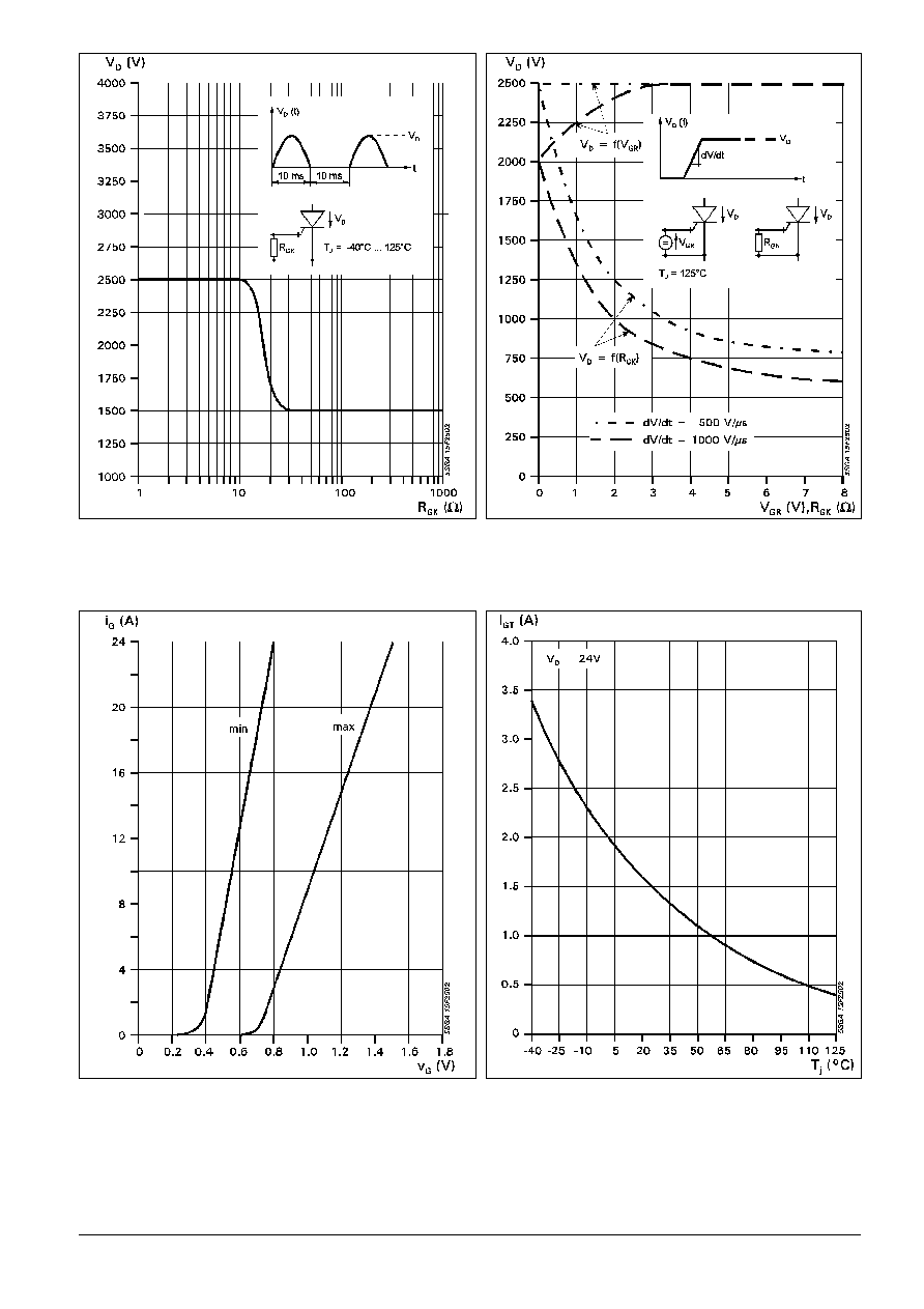
Fig. 5
Forward blocking voltage vs. gate-cathode
resistance.
Fig. 6 Static dv/dt capability: Forward blocking
voltage vs. neg. gate voltage or gate
cathode resistance.
Fig. 7 Forwarde gate current vs. forard gate
voltage.
Fig. 8 Gate trigger current vs. junction
temperature

5SGA 15F2502
ABB Semiconductors AG reserves the right to change specifications without notice.
Doc. No. 5SYA 1214-01 Aug. 2000
page 6 of 9
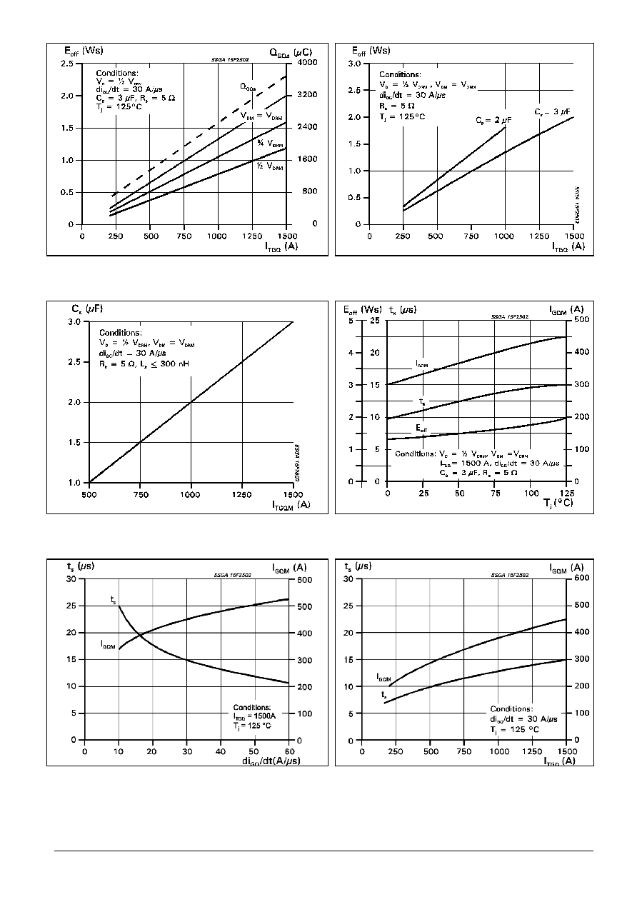
Fig. 9 Turn-on energy per pulse vs. on-state
current and turn-on voltage.
Fig. 10 Turn-on energy per pulse vs. on.-state
current and current rise rate
Common Test conditions for figures 9, 10 and 11:
di
G
/dt
= 20 A/µs
C
S
= 3 µF
R
S
=
5
Tj =
125
∞C
Definition of Turn-on energy:
)
0.1
I
0,
(t
G
20
0
GM
T
s
D
on
I
dt
I
V
E
=
=
=
µ
Common Test conditions for figures 12, 13 and 15:
Definition of Turn-off energy:
)
0.9
I
0,
t
(
T
40
0
TGQ
T
s
D
off
I
dt
I
V
E
=
=
=
µ
Fig. 11 Turn-on energy per pulse vs. on-state
current and turn-on voltage.
5SGA 15F2502
ABB Semiconductors AG reserves the right to change specifications without notice.
Doc. No. 5SYA 1214-01 Aug. 2000
page 7 of 9
Fig. 12 Turn-off energy per pulse vs. turn-off current
and peak turn-off voltage. Extracted gate
charge vs. turn-off current.
Fig. 13 Turn-off energy per pulse vs. turn-off
current and snubber capacitance.
Fig. 14 Required snubber capacitor vs. max
allowable turn-off current.
Fig. 15 Turn-off energy per pulse, storage time
and peak turn-off gate current vs. junction
temperature
Fig. 16 Storage time and peak turn-off gate current
vs. neg. gate current rise rate.
Fig. 17 Storage time and peak turn-off gate
current vs. turn-off current
5SGA 15F2502
ABB Semiconductors AG reserves the right to change specifications without notice.
Doc. No. 5SYA 1214-01 Aug. 2000
page 8 of 9
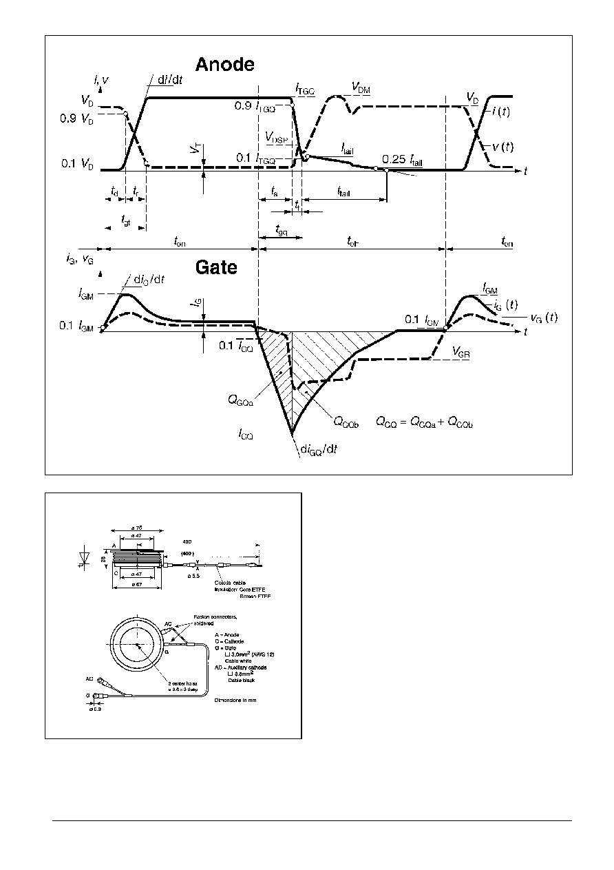
Fig. 18 General current and voltage waveforms with GTO-specific symbols
Fig. 19 Outline drawing. All dimensions are in
millimeters and represent nominal values
unless stated otherwise.

5SGA 15F2502
ABB Semiconductors AG reserves the right to change specifications without notice.
ABB Semiconductors AG
Doc. No. 5SYA 1214-01 Aug. 2000
Fabrikstrasse 2
CH-5600 Lenzburg, Switzerland
Tel:
+41 (0)62 888 6419
Fax:
+41 (0)62 888 6306
E-mail
info@ch.abb.com
Internet
www.abbsem.com
Reverse avalanche capability
In operation with an antiparallel freewheeling diode, the GTO reverse voltage
V
R
may exceed the rate
value V
RRM
due to stray inductance and diode turn-on voltage spike at high di/dt. The GTO is then
driven into reverse avalanche. This condition is not dangerous for the GTO provided avalanche time
and current are below 10 µs and 1000 A respectively. However, gate voltage must remain negative
during this time. Recommendation : V
GR
= 10... 15 V.