
ABB Switzerland Ltd, Semiconductors reserves the right to change specifications without notice.
V
DRM
=
4500 V
I
TGQM
=
3000 A
I
TSM
=
24◊10
3
A
V
T0
=
2.2 V
r
T
=
0.6 m
V
Dclink
=
2800 V
Asymmetric Gate turn-off
Thyristor
5SGA 30J4502
Doc. No. 5SYA1202-03 Jan. 03
∑
∑
∑
∑ Patented free-floating silicon technology
∑
∑
∑
∑ Low on-state and switching losses
∑
∑
∑
∑ Annular gate electrode
∑
∑
∑
∑ Industry standard housing
∑
∑
∑
∑ Cosmic radiation withstand rating
Blocking
Maximum rated values
1)
Parameter
Symbol Conditions
min
typ
max
Unit
Repetitive peak off-state
voltage
V
DRM
V
GR
2 V
4500
V
Repetitive peak reverse
voltage
V
RRM
17
V
Permanent DC voltage for
100 FIT failure rate
V
Dclink
Ambient cosmic radiation at sea level
in open air.
2800
V
Characteristic values
Parameter
Symbol Conditions
min
typ
max
Unit
Repetitive peak off-state
current
I
DRM
V
D
= V
DRM
, V
GR
2 V
60
mA
Repetitive peak reverse
current
I
RRM
V
R
= V
RRM
, R
GK
=
20
mA
Mechanical data
Maximum rated values
1)
Parameter
Symbol Conditions
min
typ
max
Unit
Mounting force
F
m
36
40
44
kN
Characteristic values
Parameter
Symbol Conditions
min
typ
max
Unit
Pole-piece diameter
D
p
± 0.1 mm
75
mm
Housing thickness
H
± 0.5 mm
26
mm
Weight
m
1.3
kg
Surface creepage distance D
s
Anode to Gate
33
mm
Air strike distance
D
a
Anode to Gate
15
mm
1) Maximum rated values indicate limits beyond which damage to the device may occur

5SGA 30J4502
ABB Switzerland Ltd, Semiconductors reserves the right to change specifications without notice.
Doc. No. 5SYA1202-03 Jan. 03
page 2 of 9
GTO Data
On-state
Maximum rated values
1)
Parameter
Symbol Conditions
min
typ
max
Unit
Max. average on-state
current
I
TAVM
Half sine wave, T
C
= 85 ∞C
930
A
Max. RMS on-state current I
TRMS
1460
A
Max. peak non-repetitive
surge current
I
TSM
24◊10
3
A
Limiting load integral
I
2
t
t
p
= 10 ms, T
vj
= 125∞C, sine wave
After Surge: V
D
= V
R
= 0 V
2.88◊10
6
A
2
s
Max. peak non-repetitive
surge current
I
TSM
40◊10
3
A
Limiting load integral
I
2
t
t
p
= 1 ms, T
vj
= 125∞C, sine wave
After Surge: V
D
= V
R
= 0 V
800◊10
3
A
2
s
Characteristic values
Parameter
Symbol Conditions
min
typ
max
Unit
On-state voltage
V
T
I
T
= 3000 A, T
vj
= 125∞C
4
V
Threshold voltage
V
(T0)
2.2
V
Slope resistance
r
T
T
vj
= 125∞C
I
T
= 300...4000 A
0.6
m
Holding current
I
H
T
vj
= 25∞C
50
A
Turn-on switching
Maximum rated values
1)
Parameter
Symbol Conditions
min
typ
max
Unit
Critical rate of rise of on-
state current
di
T
/dt
cr
f = 200 Hz
400
A/µs
Critical rate of rise of on-
state current
di
T
/dt
cr
T
vj
= 125∞C,
I
T
= 3000 A, I
GM
= 30 A,
di
G
/dt = 20 A/µs
f = 1 Hz
800
A/µs
Min. on-time
t
on
100
µs
Characteristic values
Parameter
Symbol Conditions
min
typ
max
Unit
Turn-on delay time
t
d
3
µs
Rise time
t
r
6
µs
Turn-on energy per pulse
E
on
V
D
= 0.5 V
DRM
, T
vj
= 125 ∞C
I
T
= 3000 A, di/dt = 200 A/µs,
I
GM
= 30 A, di
G
/dt = 20 A/µs, C
S
= 6
µF, R
S
= 5
3.6
J
Turn-off switching
Maximum rated values
1)
Parameter
Symbol Conditions
min
typ
max
Unit
Max. controllable turn-off
current
I
TGQM
V
DM
V
DRM
, di
GQ
/dt = 40 A/µs,
C
S
= 6 µF, L
S
0.3 µH
3000
A
Min. off-time
t
off
80
µs
Characteristic values
Parameter
Symbol Conditions
min
typ
max
Unit
Storage time
t
S
25
µs
Fall time
t
f
3
µs
Turn-on energy per pulse
E
off
13
J
Peak turn-off gate current
I
GQM
V
D
= 0.5 V
DRM
, T
vj
= 125 ∞C
V
DM
V
DRM
, di
GQ
/dt = 40 A/µs,
I
TGQ
= I
TGQM
,
R
S
= 5
, C
S
= 6 µF, L
S
= 0.3 µH
900
A

5SGA 30J4502
ABB Switzerland Ltd, Semiconductors reserves the right to change specifications without notice.
Doc. No. 5SYA1202-03 Jan. 03
page 3 of 9
Gate
Maximum rated values
1)
Parameter
Symbol Conditions
min
typ
max
Unit
Repetetive peak reverse
voltage
V
GRM
17
V
Repetetive peak reverse
current
I
GRM
V
GR
= V
GRM
20
mA
Characteristic values
Parameter
Symbol Conditions
min
typ
max
Unit
Gate trigger voltage
V
GT
1
V
Gate trigger current
I
GT
T
vj
= 25∞C,
V
D
= 24 V, R
A
= 0.1
3
A
Thermal
Maximum rated values
1)
Parameter
Symbol
Conditions
min
typ
max
Unit
Junction operating temperature
T
vj
-40
125
∞C
Storage temperature range
T
stg
-40
125
∞C
Characteristic values
Parameter
Symbol
Conditions
min
typ
max
Unit
R
th(jc)
Double side cooled
12
K/kW
R
th(jc)A
Anode side cooled
22
K/kW
Thermal resistance junction to case
R
th(jc)C
Cathode side cooled
27
K/kW
R
th(ch)
Single side cooled
6
K/kW
Thermal resistance case to heatsink
(Double side cooled)
R
th(ch)
Double side cooled
3
K/kW
Analytical function for transient thermal
impedance:
)
e
-
(1
R
=
(t)
Z
n
1
i
t/
-
i
thJC
i
Â
=
i
1
2
3
4
R
i
(K/kW)
5.400
4.500
1.700
0.400
i
(s)
1.2000
0.1700
0.0100
0.0010
Fig. 1 Transient thermal impedance, junction to
case.

5SGA 30J4502
ABB Switzerland Ltd, Semiconductors reserves the right to change specifications without notice.
Doc. No. 5SYA1202-03 Jan. 03
page 4 of 9
0
500
1000
1500
2000
2500
3000
1.0
1.5
2.0
2.5
3.0
3.5
4.0
V
T
[V]
I
T
[A]
125∞C
25∞C
0.00
0.50
1.00
1.50
2.00
2.50
3.00
3.50
4.00
4.50
5.00
0
250
500
750
1000
1250
1500
I
TAV
[V]
P
AV
[kW]
DC
180∞ Rect.
180∞ Sine
120∞ Rect.
60∞ Rect.
Fig. 2 On-state characteristics.
Fig. 3 Average on-state power dissipation vs.
average on-state current..
1.00
10.00
100.00
0
1
10
100
t
p
[ms]
I
TSM
[kA]
1.E+05
1.E+06
1.E+07
Ú
Ú
Ú
Úi
2
dt [A
2
s]
Conditions:
Before surge: T
j
= 125∞C
After surge: V
D
= 0V
I
tsm
ÚI
2
td
Fig. 4 Surge current and fusing integral vs. pulse
width.
5SGA 30J4502
ABB Switzerland Ltd, Semiconductors reserves the right to change specifications without notice.
Doc. No. 5SYA1202-03 Jan. 03
page 5 of 9
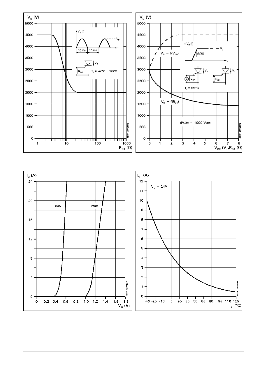
Fig. 5 Forward blocking voltage vs. gate-cathode
resistance..
Fig. 6 Static dv/dt capability: Forward blocking
voltage vs. neg. gate voltage or gate cathode
resistance.
Fig. 7 Forward gate current vs. forard gate voltage.
Fig. 8 Gate trigger current vs. junction temperature