ABB Semiconductors AG reserves the right to change specifications without notice.
V
DRM
=
6000 V
V
RRM
=
6000 V
I
TGQM
=
800 A
V
T0
=
3.25 V
r
T
=
6.4 m
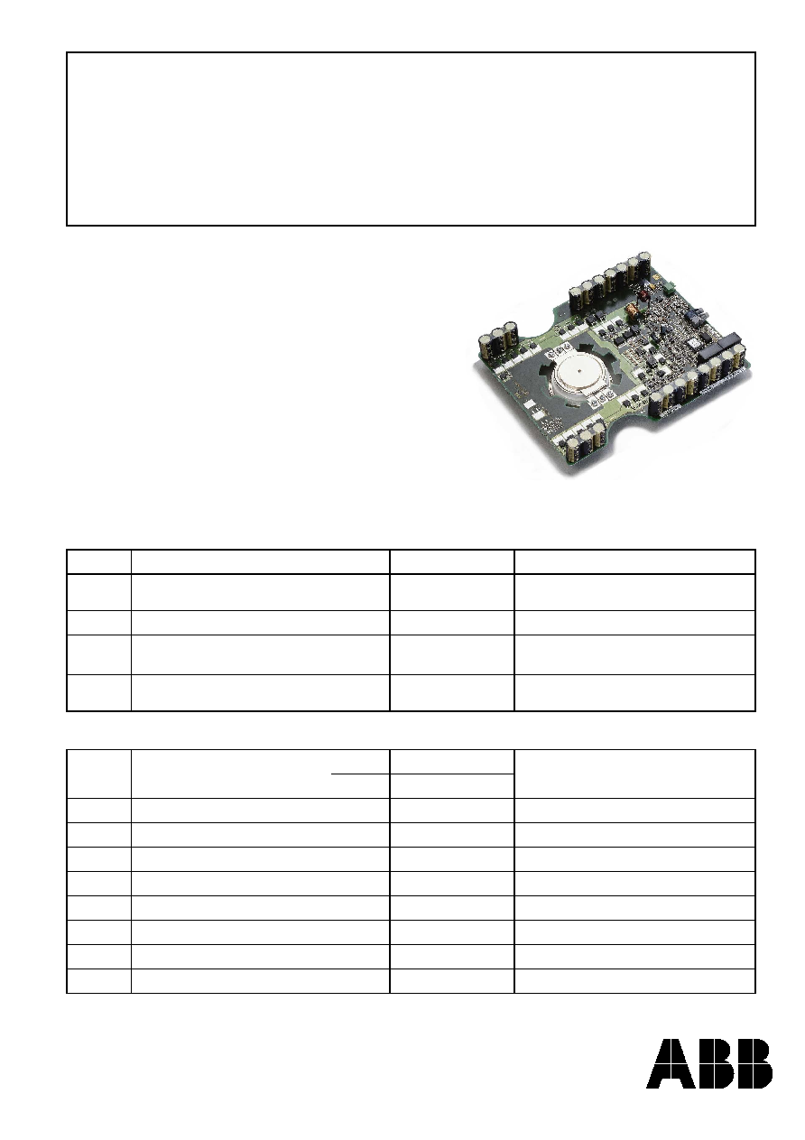
Reverse Blocking Integrated
Gate-Commutated Thyristor
5SHZ 08F6000
Doc. No. 5SYA1231-01 Sep. 01
∑
∑
∑
∑ Optimized for current source inverter (CSI)
∑
∑
∑
∑ Fast response (t
don
< 3 µs, t
doff
< 7 µs)
∑
∑
∑
∑ Precise timing (t
doff
< 400 ns)
∑
∑
∑
∑ Direct fiber optic control
∑
∑
∑
∑ Status feedback
∑
∑
∑
∑ Cosmic radiation withstand rating
∑
∑
∑
∑ Very high EMI immunity
Blocking
V
DRM
Repetitive peak off-state voltage
6000 V
V
RRM
Reverse repetitive peak off-state
voltage
6000 V
I
DRM
Repetitive peak off-state current
50 mA
V
D
= V
DRM
I
RRM
Reverse repetitive peak off-state
current
50 mA
V
R
= V
RRM
V
AC
Max. AC voltage for 100
FIT failure rate
3600 V
0
T
jop
125 ∞C. Ambient cosmic
radiation at sea level in open air.
Mechanical data
(see Fig. 8)
min.
12 kN
F
m
Mounting force
max.
16 kN
D
p
Pole-piece diameter
47 mm
±0.1 mm
H
Housing thickness
26 mm
±0.5 mm
m
Weight IGCT
1.00 kg
D
S
Surface creepage distance
33 mm
D
a
Air strike distance
13 mm
l
Length IGCT
250 mm
+0/-0.5 mm
h
Height IGCT
44 mm
±1.0 mm
w
Width IGCT
208 mm
+0/-0.5 mm

5SHZ 08F6000
ABB Semiconductors AG reserves the right to change specifications without notice.
Doc. No. 5SYA1231-01 Sep. 01
page 3 of 8
On-state
(see Fig. 2)
I
TAVM
Max. average on-state current
290 A
I
TRMS
Max. RMS on-state current
450 A
Half sine wave, T
C
= 85 ∞C
V
T
On-state voltage
8.40 V
I
T
=
800 A
V
T0
Threshold voltage
3.25 V
T
j
= 125 ∞C
r
T
Slope resistance
6.4 m
I
T
=
200 - 800 A
Self commutation (V
D
> 0 V)
Turn-on switching (see Fig. 3, 10, 11)
di/dt
crit
Max. rate of rise of on-state
current
1300 A/µs
T
j
= 0...125 ∞C
t
on (min)
Min. on-time
10 µs
t
don
Turn-on delay time
3 µs
V
D
=
3000 V
T
j
=
125 ∞C
t
r
Rise time
1.5 µs
I
T
=
800 A
di/dt =
500 A/µs
E
on
Turn-on energy per pulse
0.8 J
R
S
=
10
L
comm
=
6 µH
C
S
=
0.1 µF
L
S
=
350 nH
Turn-off switching (see Fig. 4, 6, 10, 11)
I
TGQM
Max. contr. turn-off current
800 A
T
j
= 0...125 ∞C
t
off (min)
Min. off-time
10 µs
t
f
Fall time
4.0 µs
V
D
=
3000 V
T
j
=
125 ∞C
t
doff
Turn-off delay time
7.0 µs
I
TGQ
=
800 A
V
DM
V
DRM
E
off
Turn-off energy per pulse
7.2 J
R
S
=
10
L
comm
=
6 µH
C
S
=
0.1 µF
L
S
=
350 nH
Load commutation (V
D
< 0 V)
Turn-off switching (see Fig. 5, 6, 10, 11)
di/dt
crit
Max. rate of rise of on-state
current
1300 A/µs
T
j
= 0...125 ∞C
I
rr
Reverse recovery current
750 A
V
D
=
-3000 V
T
j
=
125 ∞C
Q
rr
Reverse recovery charge
1500 µC
I
T
=
800 A
di/dt =
500 A/µs
E
rr
Turn off energy per pulse
6.0 J
R
S
=
10
L
comm
=
6 µH
C
S
=
0.1 µF
L
S
=
350 nH
V
RM
V
RRM

5SHZ 08F6000
ABB Semiconductors AG reserves the right to change specifications without notice.
Doc. No. 5SYA1231-01 Sep. 01
page 4 of 8
Gate Unit
Gate Unit
Power supply (see Fig. 7 to 10)
V
GDC
Gate Unit supply voltage
20
±0.5 V
DC
Without galvanic isolation to power
circuit.
P
Gin
Gate Unit power consumption
58 W
f
S
= 750 Hz, I
TGQ
= 400 A,
= 0.33
X1
Gate Unit power connector
Phoenix, Type MSTB 2.5/2-G-5.08 Au
Note 1
Optical control input/output (see Fig. 8 to 10)
P
on CS
Optical input power
>
-20 dBm
P
off CS
Optical noise power
<
-45 dBm
P
on SF
Optical output power
>
-15 dBm
P
off SF
Optical noise power
<
-50 dBm
Valid for 1mm plastic optical fibre
(POF)
t
GLITCH
Pulse width threshold
400 ns
Max. pulse width without response
CS
Receiver for command signal
Agilent, Type HFBR-2528
Note 2
SF
Transmitter for status feedback
Agilent, Type HFBR-1528
Note 2
Visual feedback (see Fig. 8, 9)
LED1 (green)
Power supply voltage ok
"Light" when power supply is within specified rang
LED2 (green)
Gate-cathode interface ok
"Light" when no short circuit, no open and mouning
force is applied.
LED3 (yellow)
Off gated
"Light" when gate-current is flowing
LED4 (red)
Off gated
"Light" when GCT is off
LED5 (red)
Not ready (failure)
(optional)
Note 1: Phoenix Contact, www.phoenixcontact.com
Note 2: Agilent Technologies, www.semiconductor.agilent.com
5SHZ 08F6000
ABB Semiconductors AG reserves the right to change specifications without notice.
Doc. No. 5SYA1231-01 Sep. 01
page 5 of 8
Thermal
T
j
Operating junction temperature range
0...125 ∞C
T
stg
Storage temperature range
-40...60 ∞C
T
amb
Ambient operational temperature range
0...60 ∞C
R
thJC
Thermal resistance junction to case
23 K/kW
Double side cooled
R
thCH
Thermal resistance case to heatsink
7.5 K/kW
Double side cooled
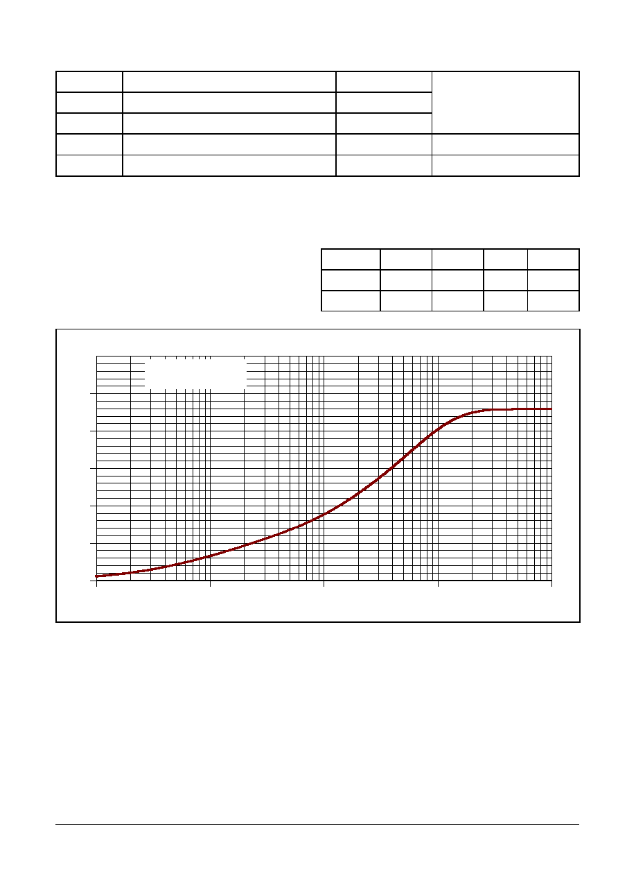
i
1
2
3
4
R
i
(K/kW)
15.5
3.35
2.92
1.17
Analytical function for transient thermal
impedance:
)
e
-
(1
R
=
(t)
Z
4
1
i
/
t
-
thJC
i
Â
=
i
i
(s)
0.57
0.087
0.013
0.0035
10
-3
10
-2
10
-1
10
0
10
1
2
3
4
5 6 7 8
2
3
4
5 6 7 8
2
3
4
5 6 7 8
2
3
4
5 6 7 8
t [s]
0
5
10
15
20
25
Z
thJC
[K/kW]
F
m
= 12...16 kN
Double side cooled
Fig. 1 Transient thermal impedance (junction-to-case) vs. time (max. values).
5SHZ 08F6000
ABB Semiconductors AG reserves the right to change specifications without notice.
Doc. No. 5SYA1231-01 Sep. 01
page 6 of 8
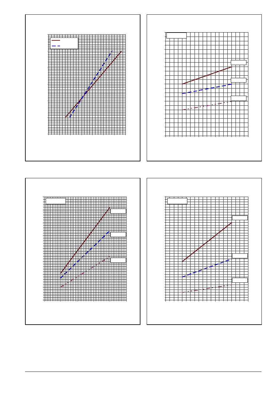
0
200
400
600
800
1000
1200
3.0
4.0
5.0
6.0
7.0
8.0
9.0
10.0
V
T
[V]
I
T
[A]
Tj = 125∞C
Tj = 25∞C
0.0
0.2
0.4
0.6
0.8
1.0
1.2
0
200
400
600
800
1000
I
T
[A]
E
on
[J]
V
D
= 1000V
T
j
= 125 ∞C
V
D
= 2000V
V
D
= 3000V
Fig. 2 On-state characteristics.
Fig. 3 Turn-on energy per pulse
Self commutation (V
D
> 0 V)
0.0
1.0
2.0
3.0
4.0
5.0
6.0
7.0
8.0
0
200
400
600
800
1000
I
TGQ
[A]
E
off
[A]
V
D
= 1000V
T
j
= 125 ∞C
V
D
= 2000V
V
D
= 3000V
0.0
1.0
2.0
3.0
4.0
5.0
6.0
7.0
8.0
0
200
400
600
800
1000
I
T
[A]
E
rr
[J]
V
D
= 1000V
T
j
= 125 ∞C
V
D
= 2000V
V
D
= 3000V
Fig. 4 Turn-off energy per pulse
Self commutation (V
D
> 0 V).
Fig. 5 Turn-off energy per pulse
Load commutation (V
D
< 0 V).
5SHZ 08F6000
ABB Semiconductors AG reserves the right to change specifications without notice.
Doc. No. 5SYA1231-01 Sep. 01
page 7 of 8
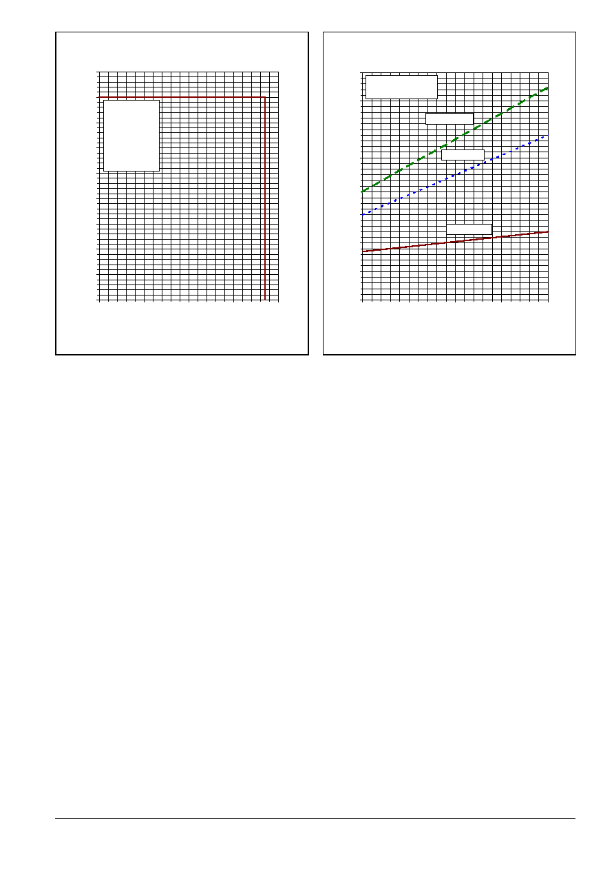
0
100
200
300
400
500
600
700
800
900
0
1000
2000
3000
4000
V
D
[V]
I
TGQ
[A]
T
j
= 0..125 ∞C
V
DM
V
DRM
V
RM
V
RRM
L
comm
= 3...6
µ
µ
µ
µH
C
s
= 0.1
µ
µ
µ
µF
R
s
= 5...10
0
10
20
30
40
50
60
70
80
0
100
200
300
400
I
TGQ
[A]
P
Gin
[W]
f
s
= 1000 Hz
duty cycle
= 0.33
VD > 0 V
f
s
= 750 Hz
f
s
= 250 Hz
Fig. 6 Max. repetitive turn-off current.
Fig. 7 Gate Unit power consumption.

5SHZ 08F6000
ABB Semiconductors AG reserves the right to change specifications without notice.
Doc. No. 5SYA1231-01 Sep. 01
page 8 of 8
Fig. 8 Device Outline Drawing.
Logic
Monitoring
Turn-
Off
Circuit
Turn-
On
Circuit
Gate
Cathode
Internal Supply (without galvanic isolation to power circuit)
Supply (20V
DC
)
X1
CS
LED1
LED2
LED3
LED4
LED5
Rx
Command Signal (Light)
Tx
Status Feedback (Light)
Anode
Gate Unit
RB-GCT
SF
Fig. 9 Block diagram RB-IGCT.

5SHZ 08F6000
ABB Semiconductors AG reserves the right to change specifications without notice.
ABB Semiconductors AG
Doc. No. 5SYA1231-01 Sep. 01
Fabrikstrasse 3
CH-5600 Lenzburg, Switzerland
Telephone +41 (0)62 888 6419
Fax
+41 (0)62 888 6306
Email
abbsem@ch.abb.com
Internet
www.abbsem.com
Turn-on (V
D
> 0 V)
Turn-off (V
D
> 0 V)
Turn-off (V
D
< 0 V)
CS
CS
V
D
I
T
0.1 V
D
0.9 V
D
V
G
di/dt
t
don
t
r
t
doff
t
f
I
T
0.8 I
TGQ
0.3 I
TGQ
V
D
V
DM
V
G
V
D
V
G
I
T
I
rr
Q
rr
di/dt
Fig. 10General current and voltage waveforms with RB-IGCT specific symbols.
Ω L
comm
L
d
L
S
R
S
C
S
L
S
R
S
C
S
DUT1
DUT2
+
C
DC
Ω L
comm
Fig. 11Test circuit.