
ABB Semiconductors AG reserves the right to change specifications without notice.
V
DSM
=
5200 V
I
TAVM
=
3875 A
I
TRMS
=
6090 A
I
TSM
=
55000 A
V
T0
=
1.03 V
r
T
=
0.160 m
Phase Control Thyristor
5STP 34Q5200
Doc. No. 5SYA1052-01 Sep. 01
∑
Patented free-floating silicon technology
∑
Low on-state and switching losses
∑
Designed for traction, energy and industrial applications
∑
Optimum power handling capability
∑
Interdigitated amplifying gate
Blocking
Part Number
5STP
5STP 34Q5000 5STP 34Q4600 Conditions
V
DSM
V
RSM
5200 V
5000 V
4600 V
f = 5 Hz, t
p
= 10ms
V
DRM
V
RRM
4400 V
4200 V
4000 V
f = 50 Hz, t
p
= 10ms
V
RSM1
5700 V
5500 V
5100 V
t
p
= 5ms, single pulse
I
DSM
500 mA
V
DSM
I
RSM
500 mA
V
RSM
T
j
= 125∞C
dV/dt
crit
2000 V/µs
Exp. to 0.67 x V
DRM
, T
j
= 125∞C
V
DRM
/ V
RRM
are equal to V
DSM
/ V
RSM
values up to T
j
= 110∞C
Mechanical data
F
M
Mounting force
nom.
90 kN
min.
81 kN
max.
108 kN
a
Acceleration
Device unclamped
Device clamped
50
100
m/s
2
m/s
2
m
Weight
2.1 kg
D
S
Surface creepage distance
36 mm
D
a
Air strike distance
15 mm

5STP 34Q5200
ABB Semiconductors AG reserves the right to change specifications without notice.
Doc. No. 5SYA1052-01 Sep. 01
page 2 of 6
On-state
I
TAVM
Max. average on-state current
3875 A
Half sine wave, T
C
= 70∞C
I
TRMS
Max. RMS on-state current
6090 A
I
TSM
Max. peak non-repetitive
55000 A
tp =
10 ms
T
j
= 125∞C
surge current
60000 A
tp =
8.3 ms
After surge:
I
2
t
Limiting load integral
15125 kA
2
s tp =
10 ms
V
D
= V
R
= 0V
14940 kA
2
s tp =
8.3 ms
V
T
On-state voltage
1.54 V
I
T
=
3000 A
V
T0
Threshold voltage
1.03 V
I
T
= 2300 - 7000 A
T
j
= 125∞C
r
T
Slope resistance
0.160 m
I
H
Holding current
50-125 mA
T
j
= 25∞C
20-75 mA
T
j
= 125∞C
I
L
Latching current
100-
500
mA
T
j
= 25∞C
75-250 mA
T
j
= 125∞C
Switching
di/dt
crit
Critical rate of rise of on-state
250 A/µs Cont. f = 50 Hz V
D
0.67V
DRM
, T
j
= 125∞C
current
500 A/µs
I
TRM
= 3000 A
60 sec.
f = 50Hz
I
FG
= 2 A, t
r
= 0.5 µs
t
d
Delay time
3.0 µs
V
D
= 0.4
V
DRM
I
FG
= 2 A, t
r
= 0.5 µs
t
q
Turn-off time
700 µs
V
D
0.67V
DRM
I
TRM
= 3000 A, T
j
= 125∞C
dv
D
/dt = 20V/µs V
R
> 200 V, di
T
/dt = -5 A/µs
Q
rr
Recovery charge
min
7000 µAs
max
9000 µAs
Triggering
V
GT
Gate trigger voltage
2.6 V
T
j
= 25∞
I
GT
Gate trigger current
400 mA
T
j
= 25∞
V
GD
Gate non-trigger voltage
0.3 V
V
D
=0.4 x V
DRM
I
GD
Gate non-trigger current
10 mA
V
D
= 0.4 x V
DRM
V
FGM
Peak forward gate voltage
12 V
I
FGM
Peak forward gate current
10 A
V
RGM
Peak reverse gate voltage
10 V
P
G
Gate power loss
3 W
5STP 34Q5200
ABB Semiconductors AG reserves the right to change specifications without notice.
Doc. No. 5SYA1052-01 Sep. 01
page 3 of 6
Thermal
T
jmax
Max. operating junction temperature
range
125 ∞C
T
stg
Storage temperature range
-40...140 ∞C
R
thJC
Thermal resistance
10 K/kW
Anode side cooled
junction to case
10 K/kW
Cathode side cooled
5 K/kW
Double side cooled
R
thCH
Thermal resistance case to
2 K/kW
Single side cooled
heat sink
1 K/kW
Double side cooled
Analytical function for transient thermal
impedance:
)
e
-
(1
R
=
(t)
Z
n
1
i
t/
-
i
thJC
i
Â
=
i
1
2
3
4
R
i
(K/kW)
3.27
0.736
0.661
0.312
i
(s)
0.5237
0.1082
0.02
0.0075
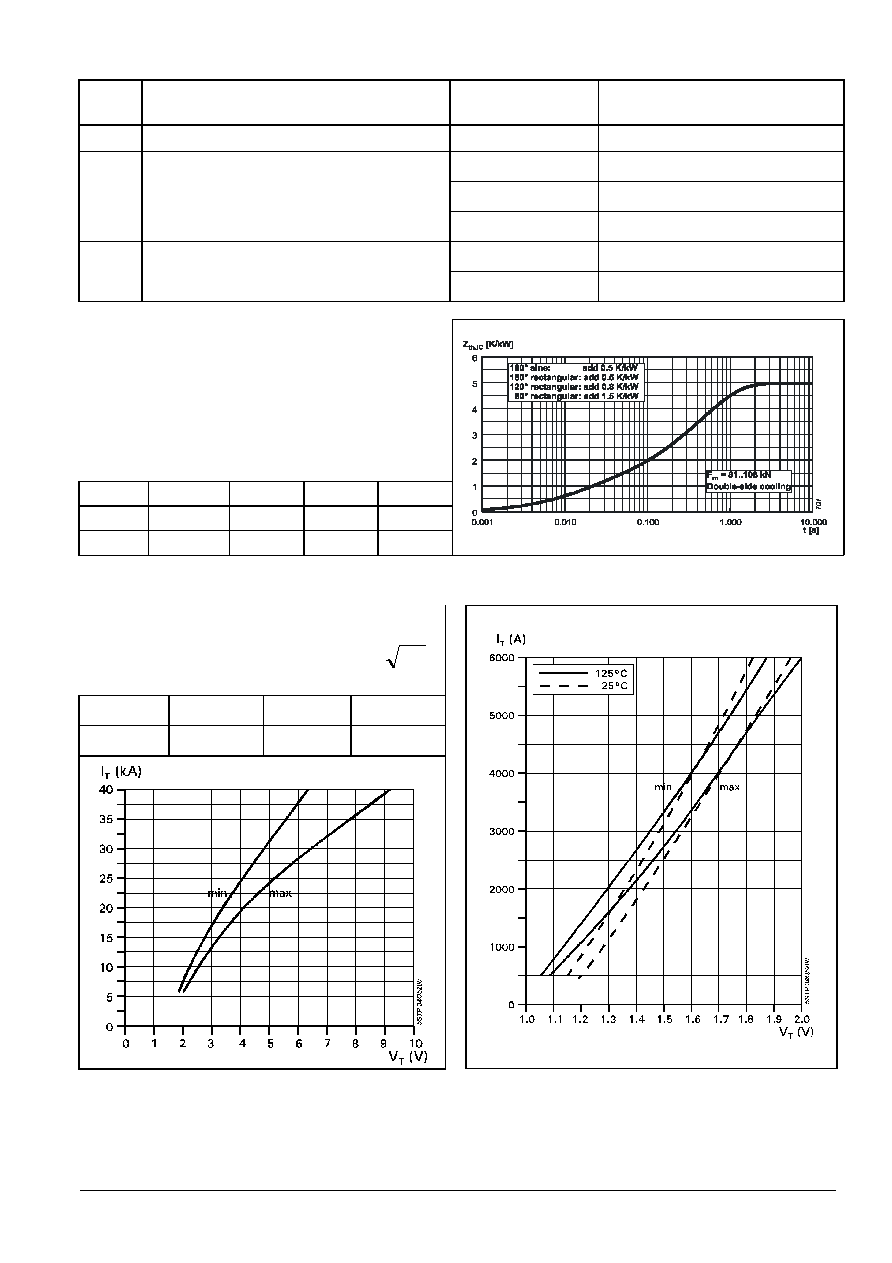
Fig. 1 Transient thermal impedance junction to case.
On-state characteristic model:
IT
D
iT
C
iT
B
A
VT
+
+
+
+
=
)
1
ln(
Valid for i
T
= 500 ≠ 14000 A
A
B
C
D
1.0649
0.000105
-0.038879
0.008155
Fig. 2 On-state characteristics.
T
j
=125∞C, 10ms half sine
Fig. 3 On-state characteristics.

5STP 34Q5200
ABB Semiconductors AG reserves the right to change specifications without notice.
Doc. No. 5SYA1052-01 Sep. 01
page 4 of 6
0
1000
2000
3000
4000
5000
6000
I
TAV
(A)
70
75
80
85
90
95
100
105
110
115
120
125
130
T
case
(∞C)
DC
180∞
rectangular
180∞
sine
120∞
rectangular
5S
T
P
3
4
Q
520
0
Double-sided
cooling
Fig. 4 On-state power dissipation vs. mean on-
state current. Turn - on losses excluded.
Fig. 5 Max. permissible case temperature vs.
mean on-state current.
Fig. 6 Surge on-state current vs. pulse length.
Half-sine wave.
Fig. 7 Surge on-state current vs. number of
pulses. Half-sine wave, 10 ms, 50Hz.

5STP 34Q5200
ABB Semiconductors AG reserves the right to change specifications without notice.
Doc. No. 5SYA1052-01 Sep. 01
page 5 of 6
Fig. 8 Gate trigger characteristics.
Fig. 9 Max. peak gate power loss.
Fig. 10 Recovery charge vs. decay rate of on-
state current.
Fig. 11 Peak reverse recovery current vs. decay
rate of on-state current.
Turn - off time, typical parameter relationship.
Fig. 12 t
q
/t
q1
= f
1
(T
j
)
Fig. 13 t
q
/t
q1
= f
2
(-di
T
/dt)
Fig. 14 t
q
/t
q1
= f
3
(dv/dt)
t
q
= t
q1
∑ f
1
(T
j
)
∑ f
2
(-di
T
/dt)
∑ f
3
(dv/dt)
t
q1
:at normalized values (see page 2)
t
q
: at varying conditions
5STP 34Q5200
ABB Semiconductors AG reserves the right to change specifications without notice.
ABB Semiconductors AG
Doc. No. 5SYA1052-01 Sep. 01
Fabrikstrasse 3
CH-5600 Lenzburg, Switzerland
Telephone +41 (0)62 888 6419
Fax
+41 (0)62 888 6306
Email
abbsem@ch.abb.com
Internet
www.abbsem.com
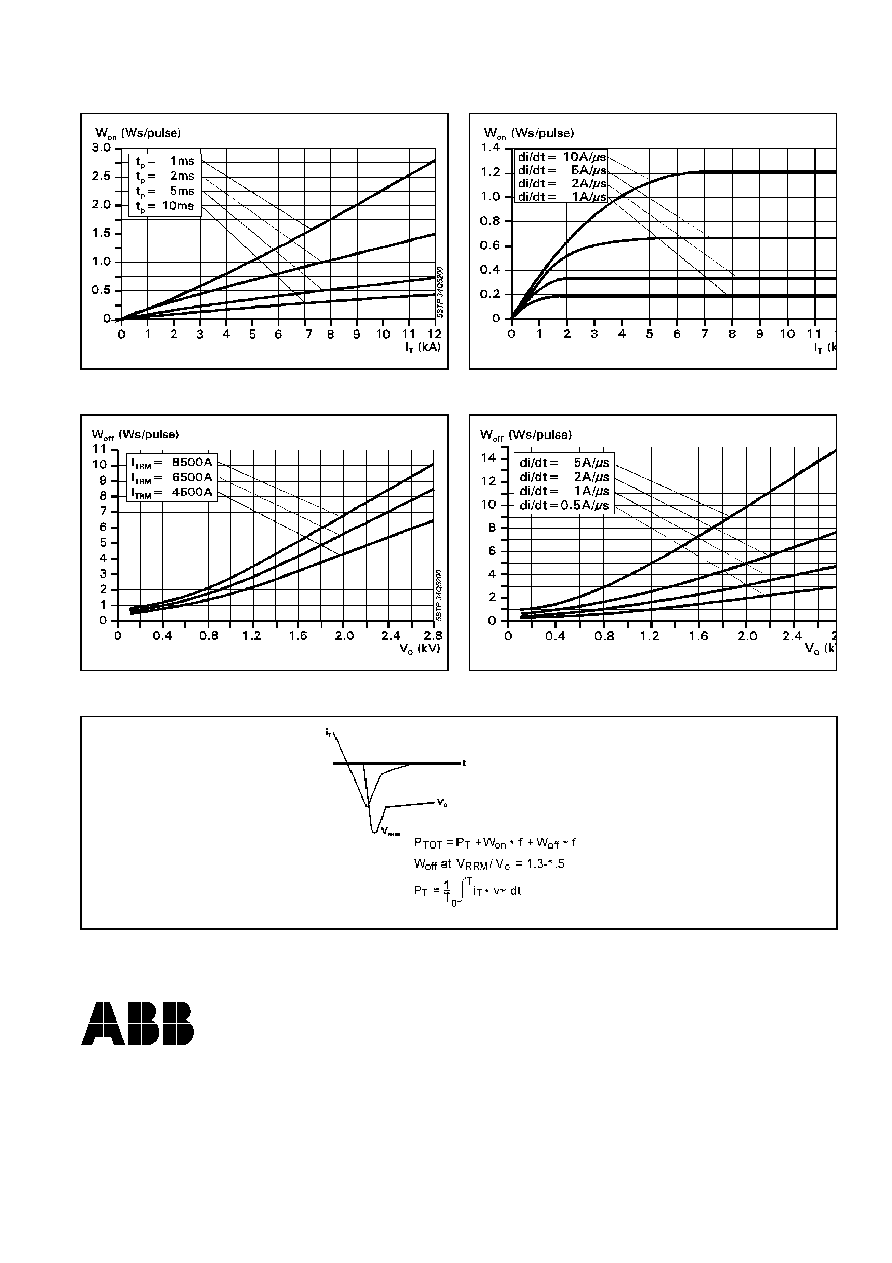
Turn-on and Turn-off losses
Fig. 15 W
on
= f(I
T
, t
P
), T
j
= 125∞C.
Half sinusoidal waves.
Fig. 16 W
on
= f(I
T
, di/dt), T
j
= 125∞C.
Rectangular waves.
Fig. 17 W
off
= f(V
0
,I
T
), T
j
= 125∞C.
Half sinusoidal waves. t
P
= 10 ms.
Fig. 18 W
off
= f(V
0
,di/dt), T
j
= 125∞C.
Rectangular waves.