 | –≠–ª–µ–∫—Ç—Ä–æ–Ω–Ω—ã–π –∫–æ–º–ø–æ–Ω–µ–Ω—Ç: A1225A-1 | –°–∫–∞—á–∞—Ç—å:  PDF PDF  ZIP ZIP |
D e c e m b e r 2 0 0 0
1
© 2000 Actel Corporation
v 4 . 0 . 1
ACT
TM
2 Family FPGAs
F e a t u r e s
∑ Up to 8000 Gate Array Gates
(20,000 PLD equivalent gates)
∑ Replaces up to 200 TTL Packages
∑ Replaces up to eighty 20-Pin PAL
Æ
Packages
∑ Design Library with over 500 Macro Functions
∑ Single-Module Sequential Functions
∑ Wide-Input Combinatorial Functions
∑ Up to 1232 Programmable Logic Modules
∑ Up to 998 Flip-Flops
∑ Datapath Performance at 105 MHz
∑ 16-Bit Accumulator Performance to 39 MHz
∑ Two In-Circuit Diagnostic Probe Pins Support Speed
Analysis to 50 MHz
∑ Two High-Speed, Low-Skew Clock Networks
∑ I/O Drive to 10 mA
∑ Nonvolatile, User Programmable
∑ Logic Fully Tested Prior to Shipment
∑ 1.0-micron CMOS Technology
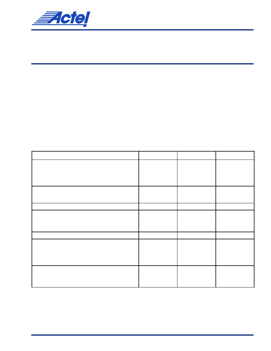
P r o d u c t F a m i l y P r o f i l e
Device
A1225A
A1240A
A1280A
Capacity
Gate Array Equivalent Gates
PLD Equivalent Gates
TTL Equivalent Packages
20-Pin PAL Equivalent Packages
2,500
6,250
63
25
4,000
10,000
100
40
8,000
20,000
200
80
Logic Modules
S-Modules
C-Modules
451
231
220
684
348
336
1,232
624
608
Flip-Flops (maximum)
382
568
998
Routing Resources
Horizontal Tracks/Channel
Vertical Tracks/Channel
PLICE Antifuse Elements
36
15
250,000
36
15
400,000
36
15
750,000
User I/Os (maximum)
83
104
140
Packages
1
100 CPGA
100 PQFP
100 VQFP
84 PLCC
132 CPGA
144 PQFP
176 TQFP
84 PLCC
176 CPGA
160 PQFP
176 TQFP
84 PLCC
172 CQFP
Performance
2
16-Bit Prescaled Counters
16-Bit Loadable Counters
16-Bit Accumulators
105 MHz
70 MHz
39 MHz
100 MHz
69 MHz
38 MHz
85 MHz
67 MHz
36 MHz
Notes:
1.
See the
"Product Plan" on page 3
for package availability.
2.
Performance is based on `≠2' speed devices at commercial worst-case operating conditions using PREP Benchmarks, Suite #1, Version 1.2,
dated 3-28-93, any analysis is not endorsed by PREP.
A C T
TM
2 F a m i l y F P G A s
2
v4.0
D e s c r i p t i o n
The ACTTM 2 family represents Actel's second generation of
field programmable gate arrays (FPGAs). The ACT 2 family
presents a two-module architecture, consisting of C-modules
and S-modules. These modules are optimized for both
combinatorial and sequential designs. Based on Actel's
patented channeled array architecture, the ACT 2 family
provides significant enhancements to gate density and
performance while maintaining downward compatibility
with the ACT 1 design environment and upward
compatibility with the ACT 3 design environment. The
devices are implemented in silicon gate, 1.0-µm, two-level
metal CMOS, and employ Actel's PLICE
Æ
antifuse
technology. This revolutionary architecture offers gate array
design flexibility, high performance, and fast
time-to-production with user programming. The ACT 2
family is supported by the Designer and Designer Advantage
Systems, which offers automatic pin assignment, validation
of electrical and design rules, automatic placement and
routing, timing analysis, user programming, and diagnostic
probe capabilities. The systems are supported on the
following platforms: 386/486TM PC, Sun
TM
, and HP
TM
workstations. The systems provide CAE interfaces to the
following design environments: Cadence, Viewlogic
Æ
,
Mentor Graphics
Æ
, and OrCADTM.
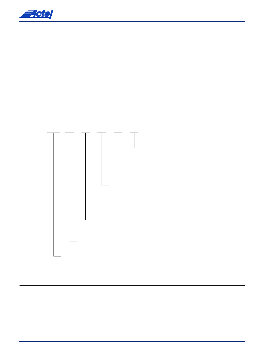
O r d e r i n g I n f o r m a t i o n
Application (Temperature Range)
C = Commercial (0 to +70∞C)
I
= Industrial (≠40 to +85∞C)
M = Military (≠55 to +125∞C)
B = MIL-STD-883
Package Type
PL = Plastic J-Leaded Chip Carrier
PQ = Plastic Quad Flat Pack
CQ = Ceramic Quad Flat Pack
PG = Ceramic Pin Grid Array
TQ = Thin (1.4 mm) Quad Flat Pack
VQ = Very Thin (1.0 mm) Quad Flat Pack
Speed Grade
Blank = Standard Speed
≠1 = Approximately 15% faster than Standard
≠2 = Approximately 25% faster than Standard
Part Number
A1225 = 2500 Gates
A1240 = 4000 Gates
A1280 = 8000 Gates
Die Revision
A = 1.0-µm CMOS process
Package Lead Count
A1280
≠
PG
176
C
1
A
v4.0
3
A C T
TM
2 F a m i l y F P G A s
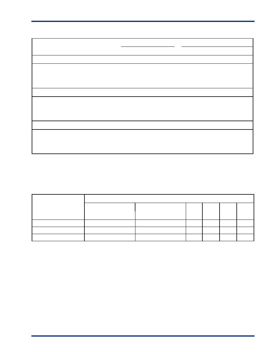
P r o d u c t P l a n
D e v i c e R e s o u r c e s
.
Speed Grade*
Application
Std
≠1
≠2
C
I
M
B
A1225A Device
100-pin Ceramic Pin Grid Array (PG)
100-pin Plastic Quad Flat Pack (PQ)
100-pin Very Thin (1.0 mm) Quad Flat Pack (VQ)
84-pin Plastic Leaded Chip Carrier (PL)
--
--
--
--
--
--
--
--
--
--
A1240A Device
132-pin Ceramic Pin Grid Array (PG)
176-pin Thin (1.4 mm) Quad Flat Pack (TQ)
144-pin Plastic Quad Flat Pack (PQ)
84-pin Plastic Leaded Chip Carrier (PL)
--
--
--
--
--
--
--
--
A1280A Device
176-pin Ceramic Pin Grid Array (PG)
176-pin Thin (1.4 mm) Quad Flat Pack (TQ)
160-pin Plastic Quad Flat Pack (PQ)
172-pin Ceramic Quad Flat Pack (CQ)
--
--
--
--
--
--
--
Contact your Actel sales representatives for product availability.
Applications:
C = Commercial
Availability:
= Available
*Speed Grade:
≠1 = Approx. 15% faster than Standard
I = Industrial
P = Planned
≠2 = Approx. 25% faster than Standard
M = Military
-- = Not Planned
B = MIL-STD-883
User I/Os
Device
Series
Logic
Modules Gates
CPGA
PQFP
PLCC
CQFP
TQFP
VQFP
176-pin 132-pin 100-pin 160-pin 144-pin 100-pin
84-pin
172-pin 176-pin 100-pin
A1225A
451
2500
--
--
83
--
--
83
72
--
--
83
A1240A
684
4000
--
104
--
--
104
--
72
--
104
--
A1280A
1232
8000
140
--
--
125
--
--
72
140
140
--
A C T
TM
2 F a m i l y F P G A s
4
v4.0
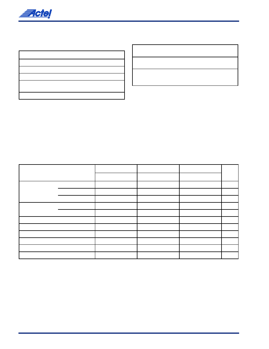
O p e r a t i n g C o n d i t i o n s
A b s o l u t e M a x i m u m R a ti n g s
1
Free air temperature range
E l e c t r i c a l Sp e c i f i c a t i o n s
R e c o m m e n d e d O p e r a t i n g C o n d i ti o n s
Symbol
Parameter
Limits
Units
V
CC
DC Supply Voltage
≠0.5 to +7.0
V
V
I
Input Voltage
≠0.5 to V
CC
+0.5
V
V
O
Output Voltage
≠0.5 to V
CC
+0.5
V
I
IO
I/O Source/Sink
Current
2
±20
mA
T
STG
Storage Temperature
≠65 to +150
∞C
Notes:
1.
Stresses beyond those listed under "Absolute Maximum
Ratings" may cause permanent damage to the device.
Exposure to absolute maximum rated conditions for extended
periods may affect device reliability. Device should not be
operated outside the Recommended Operating Conditions.
2.
Device inputs are normally high impedance and draw
extremely low current. However, when input voltage is greater
than V
CC
+ 0.5 V or less than GND ≠ 0.5 V, the internal
protection diode will be forward biased and can draw excessive
current.
Parameter
Commercia
l
Industria
l
Military
Units
Temperature
Range
1
0 to +70
≠40 to
+85
≠55 to
+125
∞C
Power
Supply
Tolerance
±5
±10
±10
%V
CC
Note:
1.
Ambient temperature (T
A
) is used for commercial and
industrial; case temperature (T
C
) is used for military.
Symbol
Parameter
Commercial
Industrial
Military
Units
Min.
Max.
Min.
Max.
Min.
Max.
V
OH
1
(I
OH
= ≠10 mA)
2
2.4
V
(I
OH
= ≠6 mA)
3.84
V
(I
OH
= ≠4 mA)
3.7
3.7
V
V
OL
1
(I
OL
= 10 mA)
2
0.5
V
(I
OL
= 6 mA)
0.33
0.40
0.40
V
V
IL
≠0.3
0.8
≠0.3
0.8
≠0.3
0.8
V
V
IH
2.0
V
CC
+ 0.3
2.0
V
CC
+ 0.3
2.0
V
CC
+ 0.3
V
Input Transition Time t
R
, t
F
2
500
500
500
ns
C
IO
I/O Capacitance
2, 3
10
10
10
pF
Standby Current, I
CC
4
(typical = 1 mA)
2
10
20
mA
Leakage Current
5
≠10
10
≠10
10
≠10
10
µA
Notes:
1.
Only one output tested at a time. V
CC
= min.
2.
Not tested, for information only.
3.
Includes worst-case 176 CPGA package capacitance. V
OUT
= 0 V, f = 1 MHz.
4.
All outputs unloaded. All inputs = V
CC
or GND, typical I
CC
= 1 mA. I
CC
limit includes I
PP
and I
SV
during normal operation.
5.
V
OUT
, V
IN
= V
CC
or GND.

v4.0
5
A C T
TM
2 F a m i l y F P G A s
P a c k a g e T h e r m a l C h a r a c t e r i s t i c s
The device junction to case thermal characteristic is
jc,
and the junction to ambient air characteristic is
ja. The
thermal characteristics for
ja are shown with two different
air flow rates.
Maximum junction temperature is 150∞C.
A sample calculation of the absolute maximum power
dissipation allowed for a PQFP 160-pin package at
commercial temperature is as follows:
P o w e r D i s s i p a t i o n
P = [I
CC
standby + I
CC
active] * V
CC
+ I
OL
* V
OL
* N +
I
OH
* (V
CC
≠ V
OH
) * M
Where:
I
CC
standby is the current flowing when no inputs or outputs
are changing.
I
CC
active is the current flowing due to CMOS switching.
I
OL
, I
OH
are TTL sink/source currents.
V
OL
, V
OH
are TTL level output voltages.
N equals the number of outputs driving TTL loads to V
OL
.
M equals the number of outputs driving TTL loads to V
OH
.
An accurate determination of N and M is problematical
because their values depend on the family type, design
details, and on the system I/O. The power can be divided
into two components: static and active.
S ta t i c P o w e r C o m p o n e n t
Actel FPGAs have small static power components that
result in lower power dissipation than PALs or PLDs. By
integrating multiple PALs/PLDs into one FPGA, an even
greater reduction in board-level power dissipation can be
achieved.
The power due to standby current is typically a small
component of the overall power. Standby power is
calculated below for commercial, worst case conditions.
I
CC
V
CC
Power
2 mA
5.25V
10.5 mW
The static power dissipated by TTL loads depends on the
number of outputs driving high or low and the DC load
current. Again, this value is typically small. For instance, a
32-bit bus sinking 4 mA at 0.33 V will generate 42 mW with
all outputs driving low, and 140 mW with all outputs driving
high. The actual dissipation will average somewhere
between as I/Os switch states with time.
A c ti v e P o w e r C o m p o n e n t
Power dissipation in CMOS devices is usually dominated by
the active (dynamic) power dissipation. This component is
frequency dependent, a function of the logic and the
external I/O. Active power dissipation results from charging
internal chip capacitances of the interconnect,
unprogrammed antifuses, module inputs, and module
outputs, plus external capacitance due to PC board traces
Package Type
Pin Count
jc
ja
Still Air
ja
300 ft/min
Units
Ceramic Pin Grid Array
100
132
176
5
5
8
35
30
23
17
15
12
∞C/W
∞C/W
∞C/W
Ceramic Quad Flat Pack
172
8
25
15
∞C/W
Plastic Quad Flat Pack
1
100
144
160
13
15
15
48
40
38
40
32
30
∞C/W
∞C/W
∞C/W
Plastic Leaded Chip Carrier
2
84
12
37
28
∞C/W
Very Thin Quad Flat Pack
3
100
12
43
35
∞C/W
Thin Quad Flat Pack
4
176
15
32
25
∞C/W
Notes:(Maximum Power in Still Air)
1.
Maximum Power Dissipation for PQFP packages are 1.9 Watts (100-pin), 2.3 Watts (144-pin), and 2.4 Watts (160-pin).
2.
Maximum Power Dissipation for PLCC packages is 2.7 Watts.
3.
Maximum Power Dissipation for VQFP packages is 2.3 Watts.
4.
Maximum Power Dissipation for TQFP packages is 3.1 Watts.
Max. junction temp. (∞C) ≠ Max. commercial temp.
ja (∞C/W)
-----------------------------------------------------------------------------------------------------------------------------
150∞C ≠ 70∞C
33∞C/W
---------------------------------
2.4 W
=
=