 | –≠–ª–µ–∫—Ç—Ä–æ–Ω–Ω—ã–π –∫–æ–º–ø–æ–Ω–µ–Ω—Ç: A54SX08-2 | –°–∫–∞—á–∞—Ç—å:  PDF PDF  ZIP ZIP |

M a y 2 0 0 0
1
© 2000 Actel Corporation
v 3 . 0
.1
54SX Family FPGAs
L e a d i n g E d g e P e r f o r m a n c e
∑ 320 MHz Internal Performance
∑ 3.7 ns Clock-to-Out (Pin-to-Pin)
∑ 0.1 ns Input Set-Up
∑ 0.25 ns Clock Skew
S p e c i f i c a ti o n s
∑ 12,000 to 48,000 System Gates
∑ Up to 249 User-Programmable I/O Pins
∑ Up to 1080 Flip-Flops
∑ 0.35µ CMOS
F e a t u r e s
∑ 66 MHz PCI
∑ CPLD and FPGA Integration
∑ Single Chip Solution
∑ 100% Resource Utilization with 100% Pin Locking
∑ 3.3V Operation with 5.0V Input Tolerance
∑ Very Low Power Consumption
∑ Deterministic, User-Controllable Timing
∑ Unique In-System Diagnostic and Debug capability with
Silicon Explorer II
∑ Boundary Scan Testing in Compliance with IEEE Standard
1149.1 (JTAG)
∑ Secure Programming Technology Prevents Reverse
Engineering and Design Theft
S X P r o d u c t P r o f i l e
A54SX08
A54SX16
A54SX16P
A54SX32
Capacity
Typical Gates
System Gates
8,000
12,000
16,000
24,000
16,000
24,000
32,000
48,000
Logic Modules
Combinatorial Cells
768
512
1,452
924
1,452
924
2,880
1800
Register Cells (Dedicated Flip-Flops)
256
528
528
1,080
Maximum User I/Os
130
175
175
249
Clocks
3
3
3
3
JTAG
Yes
Yes
Yes
Yes
PCI
--
--
Yes
--
Clock-to-Out
3.7 ns
3.9 ns
4.4 ns
4.6 ns
Input Set-Up (External)
0.8 ns
0.5 ns
0.5 ns
0.1 ns
Speed Grades
Std, ≠1, ≠2, ≠3
Std, ≠1, ≠2, ≠3
Std, ≠1, ≠2, ≠3
Std, ≠1, ≠2, ≠3
Temperature Grades
C, I, M
C, I, M
C, I, M
C, I, M
Packages (by pin count)
PLCC
PQFP
VQFP
TQFP
PBGA
FBGA
84
208
100
144, 176
--
144
--
208
100
176
--
--
--
208
100
144, 176
--
--
--
208
--
144, 176
313, 329
--
2
G e n e r a l D e s c r i p t i o n
Actel's SX family of FPGAs features a sea-of-modules
architecture that delivers device performance and
integration levels not currently achieved by any other FPGA
architecture. SX devices greatly simplify design time, enable
dramatic reductions in design costs and power
consumption, and further decrease time to market for
performance-intensive applications.
Actel's SX architecture features two types of logic modules,
the combinatorial cell (C-cell) and the register cell (R-cell),
each optimized for fast and efficient mapping of synthesized
logic functions. The routing and interconnect resources are
in the metal layers above the logic modules, providing
optimal use of silicon. This enables the entire floor of the
device to be spanned with an uninterrupted grid of
fine-grained, synthesis-friendly logic modules (or
"sea-of-modules"), which reduces the distance signals have
to travel between logic modules. To minimize signal
propagation delay, SX devices employ both local and general
routing resources. The high-speed local routing resources
(DirectConnect and FastConnect) enable very fast local
signal propagation that is optimal for fast counters, state
machines, and datapath logic. The general system of
segmented routing tracks allows any logic module in the
array to be connected to any other logic or I/O module.
Within this system, propagation delay is minimized by
limiting the number of antifuse interconnect elements to
five (90 percent of connections typically use only three
antifuses). The unique local and general routing structure
featured in SX devices gives fast and predictable
performance, allows 100 percent pin-locking with full logic
utilization, enables concurrent PCB development, reduces
design time, and allows designers to achieve performance
goals with minimum effort.
Further complementing SX's flexible routing structure is a
hard-wired, constantly loaded clock network that has been
tuned to provide fast clock propagation with minimal clock
skew. Additionally, the high performance of the internal
logic has eliminated the need to embed latches or flip-flops
in the I/O cells to achieve fast clock-to-out or fast input
set-up times. SX devices have easy-to-use I/O cells that do
not require HDL instantiation, facilitating design re-use and
reducing design and verification time.
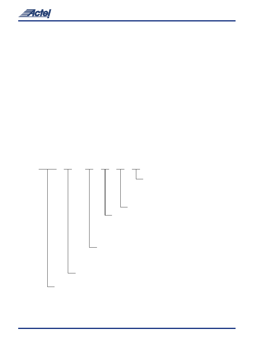
O r d e r i n g I n f o r m a t i o n
Application (Temperature Range)
Blank = Commercial (0 to +70∞C)
I = Industrial (≠40 to +85∞C)
M = Military (≠55 to +125∞C)
PP = Pre-production
Package Type
BG = Ball Grid Array
PL = Plastic Leaded Chip Carrier
PQ = Plastic Quad Flat Pack
TQ = Thin (1.4 mm) Quad Flat Pack
VQ = Very Thin (1.0 mm) Quad Flat Pack
FG = Fine Pitch Ball Grid Array (1.0 mm)
Speed Grade
Blank = Standard Speed
≠1 = Approximately 15% Faster than Standard
≠2 = Approximately 25% Faster than Standard
≠3 = Approximately 35% Faster than Standard
Part Number
A54SX08
= 12,000 System Gates
A54SX16
= 24,000 System Gates
A54SX16P = 24,000 System Gates
A54SX32
= 48,000 System Gates
Package Lead Count
A54SX16
≠
PQ
208
2
Blank = Not PCI Compliant
P = PCI Compliant
P

3
5 4 S X F a m i l y F P G A s
P r o d u c t P l a n
Speed Grade*
Application
Std
≠1
≠2
≠3
C
I
M
∑
A54SX08 Device
84-Pin Plastic Leaded Chip Carrier (PLCC)
--
100-Pin Very Thin Plastic Quad Flat Pack (VQFP)
--
144-Pin Thin Quad Flat Pack (TQFP)
--
144-Pin Fine Pitch Ball Grid Array (FBGA)
--
176-Pin Thin Quad Flat Pack (TQFP)
--
208-Pin Plastic Quad Flat Pack (PQFP)
--
A54SX16 Device
100-Pin Very Thin Plastic Quad Flat Pack (VQFP)
P
176-Pin Thin Quad Flat Pack (TQFP)
P
208-Pin Plastic Quad Flat Pack (PQFP)
P
A54SX16P Device
100-Pin Very Thin Plastic Quad Flat Pack (VQFP)
--
144-Pin Thin Quad Flat Pack (TQFP)
--
176-Pin Thin Quad Flat Pack (TQFP)
--
208-Pin Plastic Quad Flat Pack (PQFP)
--
A54SX32 Device
144-Pin Thin Quad Flat Pack (TQFP)
P
176-Pin Thin Quad Flat Pack (TQFP)
P
208-Pin Plastic Quad Flat Pack (PQFP)
P
313-Pin Plastic Ball Grid Array (PBGA)
--
329-Pin Plastic Ball Grid Array (PBGA)
--
Contact your Actel sales representative for product availability.
Applications:
C = Commercial
Availability:
= Available
*Speed Grade:
≠1 = Approx. 15% faster than Standard
I
= Industrial
P
= Planned
≠2 = Approx. 25% faster than Standard
M = Military
-- = Not Planned
≠3 = Approx. 35% faster than Standard
Only Std, ≠1, ≠2 Speed Grade
∑
Only Std, ≠1 Speed Grade
P l a s t i c D e v i c e R e s o u r c e s
User I/Os (including clock buffers)
Device
PLCC
84-Pin
VQFP
100-Pin
PQFP
208-Pin
TQFP
144-Pin
TQFP
176-Pin
PBGA
313-Pin
PBGA
329-Pin
FBGA
144-Pin
A54SX08
69
81
130
113
128
--
--
111
A54SX16
--
81
175
--
147
--
--
--
A54SX16P
--
81
175
113
147
--
--
--
A54SX32
--
--
174
113
147
249
249
--
Package Definitions (Consult your local Actel sales representative for product availability.)
PLCC = Plastic Leaded Chip Carrier, PQFP = Plastic Quad Flat Pack, TQFP = Thin Quad Flat Pack, VQFP = Very Thin Quad Flat Pack,
PBGA = Plastic Ball Grid Array, FBGA = Fine Pitch (1.0 mm) Ball Grid Array

4
S X F a m i l y A r c h i t e c t u r e
The SX family architecture was designed to satisfy
next-generation performance and integration requirements
for production-volume designs in a broad range of
applications.
P ro g ra m ma b l e I n t e r c o n n e c t E l e m e n t
The SX family provides efficient use of silicon by locating the
routing interconnect resources between the Metal 2 (M2)
and Metal 3 (M3) layers (
Figure 1
). This completely
eliminates the channels of routing and interconnect
resources between logic modules (as implemented on SRAM
FPGAs and previous generations of antifuse FPGAs), and
enables the entire floor of the device to be spanned with an
uninterrupted grid of logic modules.
Interconnection between these logic modules is achieved
using Actel's patented metal-to-metal programmable
antifuse interconnect elements, which are embedded
between the M2 and M3 layers. The antifuses are normally
open circuit and, when programmed, form a permanent
low-impedance connection.
The extremely small size of these interconnect elements
gives the SX family abundant routing resources and provides
excellent protection against design pirating. Reverse
engineering is virtually impossible because it is extremely
difficult to distinguish between programmed and
unprogrammed antifuses, and there is no configuration
bitstream to intercept.
Additionally, the interconnect (i.e., the antifuses and metal
tracks) have lower capacitance and lower resistance than
any other device of similar capacity, leading to the fastest
signal propagation in the industry.
L o g i c M o d u l e D e s i g n
The SX family architecture is described as a
"sea-of-modules" architecture because the entire floor of
the device is covered with a grid of logic modules with
virtually no chip area lost to interconnect elements or
routing. Actel's SX family provides two types of logic
modules, the register cell (R-cell) and the combinatorial
cell (C-cell).
The R-cell contains a flip-flop featuring asynchronous clear,
asynchronous preset, and clock enable (using the S0 and S1
lines) control signals (
Figure 2 on page 5
). The R-cell
registers feature programmable clock polarity selectable on
a register-by-register basis. This provides additional
flexibility while allowing mapping of synthesized functions
into the SX FPGA. The clock source for the R-cell can be
chosen from either the hard-wired clock or the routed clock.
Figure 1 ∑ SX Family Interconnect Elements
Silicon Substrate
Tungsten Plug
Contact
Metal 1
Metal 2
Metal 3
Routing Tracks
Amorphous Silicon/
Dielectric Antifuse
Tungsten Plug Via
Tungsten Plug Via

5
5 4 S X F a m i l y F P G A s
The C-cell implements a range of combinatorial functions
up to 5-inputs (
Figure 3
). Inclusion of the DB input and its
associated inverter function dramatically increases the
number of combinatorial functions that can be
implemented in a single module from 800 options in
previous architectures to more than 4,000 in the SX
architecture. An example of the improved flexibility
enabled by the inversion capability is the ability to integrate
a 3-input exclusive-OR function into a single C-cell. This
facilitates construction of 9-bit parity-tree functions with 2
ns propagation delays. At the same time, the C-cell
structure is extremely synthesis friendly, simplifying the
overall design and reducing synthesis time.
C h i p A r c h i te c tu re
The SX family's chip architecture provides a unique
approach to module organization and chip routing that
delivers the best register/logic mix for a wide variety of new
and emerging applications.
M o d u l e O r g a n i z a t i o n
Actel has arranged all C-cell and R-cell logic modules into
horizontal banks called Clusters. There are two types of
Clusters: Type 1 contains two C-cells and one R-cell, while
Type 2 contains one C-cell and two R-cells.
To increase design efficiency and device performance, Actel
has further organized these modules into SuperClusters
(
Figure 4 on page 6
). SuperCluster 1 is a two-wide grouping
of Type 1 clusters. SuperCluster 2 is a two-wide group
containing one Type 1 cluster and one Type 2 cluster. SX
devices feature more SuperCluster 1 modules than
SuperCluster 2 modules because designers typically require
significantly more combinatorial logic than flip-flops.
Figure 2 ∑ R-Cell
Figure 3 ∑ C-Cell
Direct
Connect
Input
CLKA,
CLKB,
Internal Logic
HCLK
CKS
CKP
CLRB
PSETB
Y
D
Q
Routed
Data Input
S0
S1
D0
D1
D2
D3
DB
A0
B0
A1
B1
Sa
Sb
Y