J u n e 2 0 0 3
1
© 2003 Actel Corporation
v 3 . 1
54SX Family FPGAs
L e a d i n g E d g e P e r f o r m a n c e
∑ 320 MHz Internal Performance
∑ 3.7 ns Clock-to-Out (Pin-to-Pin)
∑ 0.1 ns Input Set-Up
∑ 0.25 ns Clock Skew
S p e c i f i c a t i o n s
∑ 12,000 to 48,000 System Gates
∑ Up to 249 User-Programmable I/O Pins
∑ Up to 1080 Flip-Flops
∑ 0.35µ CMOS
F e a t u r e s
∑ 66 MHz PCI
∑ CPLD and FPGA Integration
∑ Single Chip Solution
∑ 100% Resource Utilization with 100% Pin Locking
∑ 3.3V Operation with 5.0V Input Tolerance
∑ Very Low Power Consumption
∑ Deterministic, User-Controllable Timing
∑ Unique In-System Diagnostic and Debug capability with
Silicon Explorer II
∑ Boundary Scan Testing in Compliance with IEEE Standard
1149.1 (JTAG)
∑ Secure Programming Technology Prevents Reverse
Engineering and Design Theft
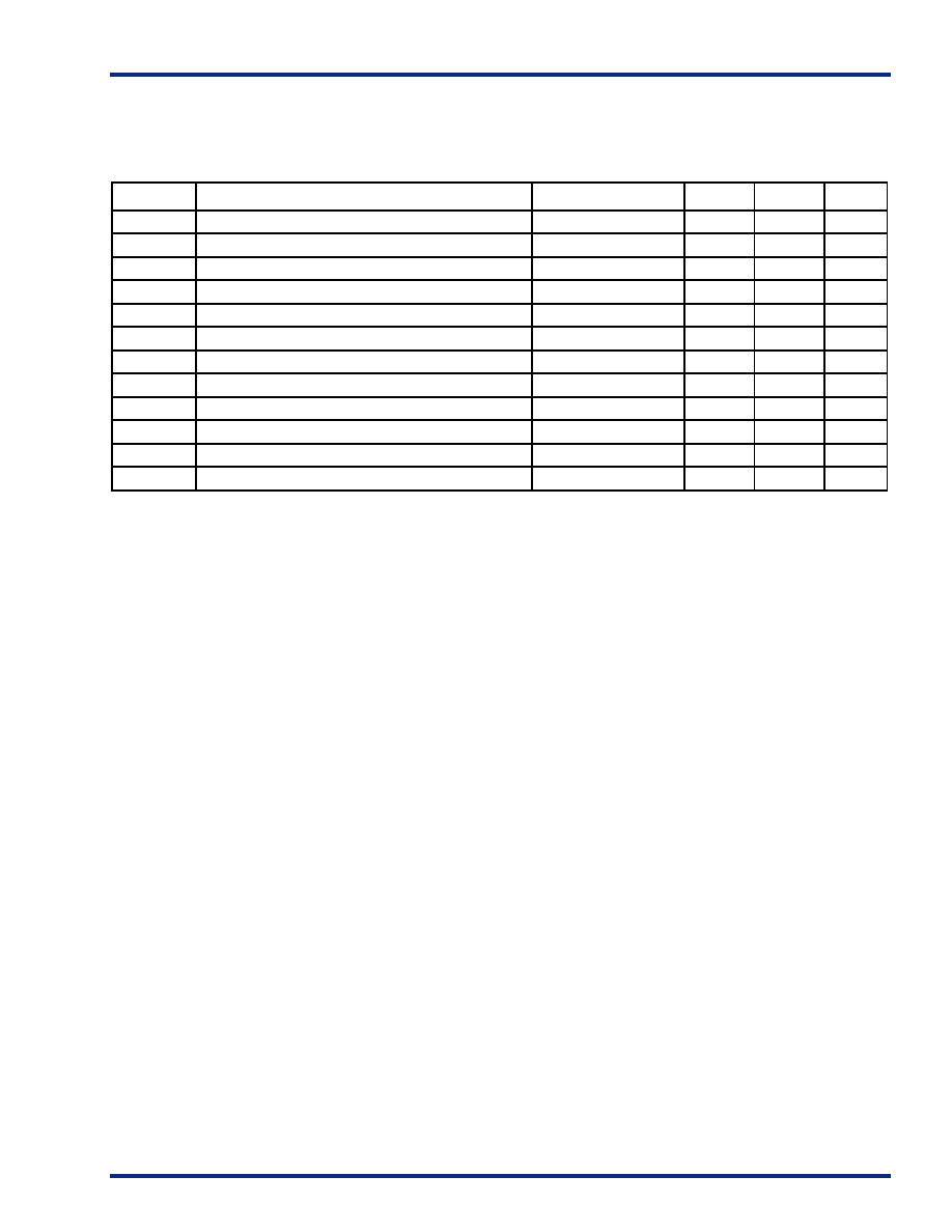
S X P r o d u c t P r o f i l e
A54SX08
A54SX16
A54SX16P
A54SX32
Capacity
Typical Gates
System Gates
8,000
12,000
16,000
24,000
16,000
24,000
32,000
48,000
Logic Modules
Combinatorial Cells
768
512
1,452
924
1,452
924
2,880
1800
Register Cells (Dedicated Flip-Flops)
256
528
528
1,080
Maximum User I/Os
130
175
175
249
Clocks
3
3
3
3
JTAG
Yes
Yes
Yes
Yes
PCI
--
--
Yes
--
Clock-to-Out
3.7 ns
3.9 ns
4.4 ns
4.6 ns
Input Set-Up (External)
0.8 ns
0.5 ns
0.5 ns
0.1 ns
Speed Grades
Std, ≠1, ≠2, ≠3
Std, ≠1, ≠2, ≠3
Std, ≠1, ≠2, ≠3
Std, ≠1, ≠2, ≠3
Temperature Grades
C, I, M
C, I, M
C, I, M
C, I, M
Packages (by pin count)
PLCC
PQFP
VQFP
TQFP
PBGA
FBGA
84
208
100
144, 176
--
144
--
208
100
176
--
--
--
208
100
144, 176
--
--
--
208
--
144, 176
313, 329
--
5 4 S X F a m i l y F P G A s
2 v3.1
G e n e r a l D e s c r i p t i o n
Actel's SX family of FPGAs features a sea-of-modules
architecture that delivers device performance and
integration levels not currently achieved by any other FPGA
architecture. SX devices greatly simplify design time, enable
dramatic reductions in design costs and power
consumption, and further decrease time to market for
performance-intensive applications.
Actel's SX architecture features two types of logic modules,
the combinatorial cell (C-cell) and the register cell (R-cell),
each optimized for fast and efficient mapping of synthesized
logic functions. The routing and interconnect resources are
in the metal layers above the logic modules, providing
optimal use of silicon. This enables the entire floor of the
device to be spanned with an uninterrupted grid of
fine-grained, synthesis-friendly logic modules (or
"sea-of-modules"), which reduces the distance signals have
to travel between logic modules. To minimize signal
propagation delay, SX devices employ both local and general
routing resources. The high-speed local routing resources
(DirectConnect and FastConnect) enable very fast local
signal propagation that is optimal for fast counters, state
machines, and datapath logic. The general system of
segmented routing tracks allows any logic module in the
array to be connected to any other logic or I/O module.
Within this system, propagation delay is minimized by
limiting the number of antifuse interconnect elements to
five (90 percent of connections typically use only three
antifuses). The unique local and general routing structure
featured in SX devices gives fast and predictable
performance, allows 100 percent pin-locking with full logic
utilization, enables concurrent PCB development, reduces
design time, and allows designers to achieve performance
goals with minimum effort.
Further complementing SX's flexible routing structure is a
hard-wired, constantly loaded clock network that has been
tuned to provide fast clock propagation with minimal clock
skew. Additionally, the high performance of the internal
logic has eliminated the need to embed latches or flip-flops
in the I/O cells to achieve fast clock-to-out or fast input
set-up times. SX devices have easy-to-use I/O cells that do
not require HDL instantiation, facilitating design re-use and
reducing design and verification time.
O r d e r i n g I n f o r m a t i o n
Application (Temperature Range)
Blank = Commercial (0 to +70∞C)
I = Industrial (≠40 to +85∞C)
M = Military (≠55 to +125∞C)
PP = Pre-production
Package Type
BG = Ball Grid Array
PL = Plastic Leaded Chip Carrier
PQ
= Plastic Quad Flat Pack
TQ = Thin (1.4 mm) Quad Flat Pack
VQ = Very Thin (1.0 mm) Quad Flat Pack
FG = Fine Pitch Ball Grid Array (1.0 mm)
Speed Grade
Blank = Standard Speed
≠1
= Approximately 15% Faster than Standard
≠2
= Approximately 25% Faster than Standard
≠3 = Approximately 35% Faster than Standard
Part Number
A54SX08
= 12,000 System Gates
A
54SX16
= 24,000 System Gates
A54SX16P = 24,000
System Gates
A
54SX32
=
48,000 System Gates
Package Lead Count
A54SX16
≠
PQ
208
2
Blank = Not PCI Compliant
P
= PCI Compliant
P
v3.1
3
5 4 S X F a m i l y F P G A s
P r o d u c t P l a n
Speed Grade*
Application
Std
≠1
≠2
≠3
C
I
M
∑
A54SX08 Device
84-Pin Plastic Leaded Chip Carrier (PLCC)
--
100-Pin Very Thin Plastic Quad Flat Pack (VQFP)
--
144-Pin Thin Quad Flat Pack (TQFP)
--
144-Pin Fine Pitch Ball Grid Array (FBGA)
--
176-Pin Thin Quad Flat Pack (TQFP)
--
208-Pin Plastic Quad Flat Pack (PQFP)
--
A54SX16 Device
100-Pin Very Thin Plastic Quad Flat Pack (VQFP)
P
176-Pin Thin Quad Flat Pack (TQFP)
P
208-Pin Plastic Quad Flat Pack (PQFP)
P
A54SX16P Device
100-Pin Very Thin Plastic Quad Flat Pack (VQFP)
--
144-Pin Thin Quad Flat Pack (TQFP)
--
176-Pin Thin Quad Flat Pack (TQFP)
--
208-Pin Plastic Quad Flat Pack (PQFP)
--
A54SX32 Device
144-Pin Thin Quad Flat Pack (TQFP)
P
176-Pin Thin Quad Flat Pack (TQFP)
P
208-Pin Plastic Quad Flat Pack (PQFP)
P
313-Pin Plastic Ball Grid Array (PBGA)
--
329-Pin Plastic Ball Grid Array (PBGA)
--
Contact your Actel sales representative for product availability.
Applications:C = CommercialAvailability:
= Available*Speed Grade:≠1
= Approx. 15% faster than Standard
I
= Industrial
P
= Planned
≠2
=
Approx. 25% faster than Standard
M
= Military
--
= Not Planned
≠3
=
Approx. 35% faster than Standard
Only Std, ≠1, ≠2 Speed Grade
∑
Only Std, ≠1 Speed Grade
P l a s t i c D e v i c e R e s o u r c e s
User I/Os (including clock buffers)
Device
PLCC
84-Pin
VQFP
100-Pin
PQFP
208-Pin
TQFP
144-Pin
TQFP
176-Pin
PBGA
313-Pin
PBGA
329-Pin
FBGA
144-Pin
A54SX08
69
81
130
113
128
--
--
111
A54SX16
--
81
175
--
147
--
--
--
A54SX16P
--
81
175
113
147
--
--
--
A54SX32
--
--
174
113
147
249
249
--
Package Definitions (Consult your local Actel sales representative for product availability.)
PLCC = Plastic Leaded Chip Carrier, PQFP = Plastic Quad Flat Pack, TQFP = Thin Quad Flat Pack, VQFP = Very Thin Quad Flat Pack,
PBGA = Plastic Ball Grid Array, FBGA = Fine Pitch (1.0 mm) Ball Grid Array
5 4 S X F a m i l y F P G A s
4 v3.1
S X F a m i l y A r c h i t e c t u r e
The SX family architecture was designed to satisfy
next-generation performance and integration requirements
for production-volume designs in a broad range of
applications.
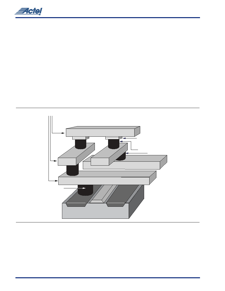
P r o g r a m m a b l e I n t e r c o n n e c t E l e m e n t
The SX family provides efficient use of silicon by locating the
routing interconnect resources between the Metal 2 (M2)
and Metal 3 (M3) layers (
Figure 1
). This completely
eliminates the channels of routing and interconnect
resources between logic modules (as implemented on SRAM
FPGAs and previous generations of antifuse FPGAs), and
enables the entire floor of the device to be spanned with an
uninterrupted grid of logic modules.
Interconnection between these logic modules is achieved
using Actel's patented metal-to-metal programmable
antifuse interconnect elements, which are embedded
between the M2 and M3 layers. The antifuses are normally
open circuit and, when programmed, form a permanent
low-impedance connection.
The extremely small size of these interconnect elements
gives the SX family abundant routing resources and provides
excellent protection against design pirating. Reverse
engineering is virtually impossible because it is extremely
difficult to distinguish between programmed and
unprogrammed antifuses, and there is no configuration
bitstream to intercept.
Additionally, the interconnect (i.e., the antifuses and metal
tracks) have lower capacitance and lower resistance than
any other device of similar capacity, leading to the fastest
signal propagation in the industry.
L o g i c M o d u l e D e s i g n
The SX family architecture is described as a
"sea-of-modules" architecture because the entire floor of
the device is covered with a grid of logic modules with
virtually no chip area lost to interconnect elements or
routing. Actel's SX family provides two types of logic
modules, the register cell (R-cell) and the combinatorial
cell (C-cell).
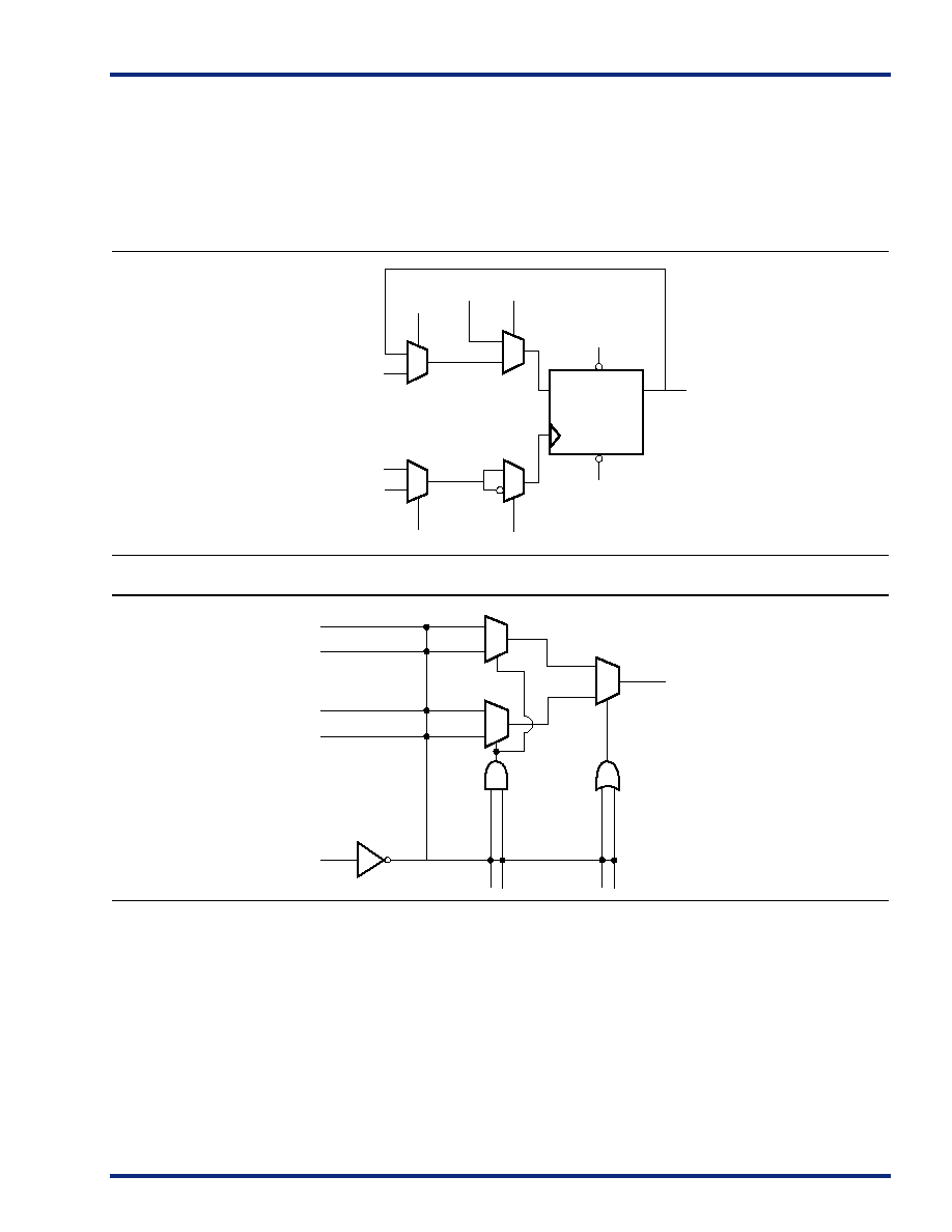
The R-cell contains a flip-flop featuring asynchronous clear,
asynchronous preset, and clock enable (using the S0 and S1
lines) control signals (
Figure 2 on page 5
). The R-cell
registers feature programmable clock polarity selectable on
a register-by-register basis. This provides additional
flexibility while allowing mapping of synthesized functions
into the SX FPGA. The clock source for the R-cell can be
chosen from either the hard-wired clock or the routed clock.
Figure 1 ∑ SX Family Interconnect Elements
Silicon Substrate
Tungsten Plug
Contact
Metal 1
Metal 2
Metal 3
Routing Tracks
Amorphous Silicon/
Dielectric Antifuse
Tungsten Plug Via
Tungsten Plug Via
v3.1
5
5 4 S X F a m i l y F P G A s
The C-cell implements a range of combinatorial functions
up to 5-inputs (
Figure 3
). Inclusion of the DB input and its
associated inverter function dramatically increases the
number of combinatorial functions that can be
implemented in a single module from 800 options in
previous architectures to more than 4,000 in the SX
architecture. An example of the improved flexibility
enabled by the inversion capability is the ability to integrate
a 3-input exclusive-OR function into a single C-cell. This
facilitates construction of 9-bit parity-tree functions with 2
ns propagation delays. At the same time, the C-cell
structure is extremely synthesis friendly, simplifying the
overall design and reducing synthesis time.
C h i p A r c h i t e c t u r e
The SX family's chip architecture provides a unique
approach to module organization and chip routing that
delivers the best register/logic mix for a wide variety of new
and emerging applications.
M o d u l e O r g a n i z a t i o n
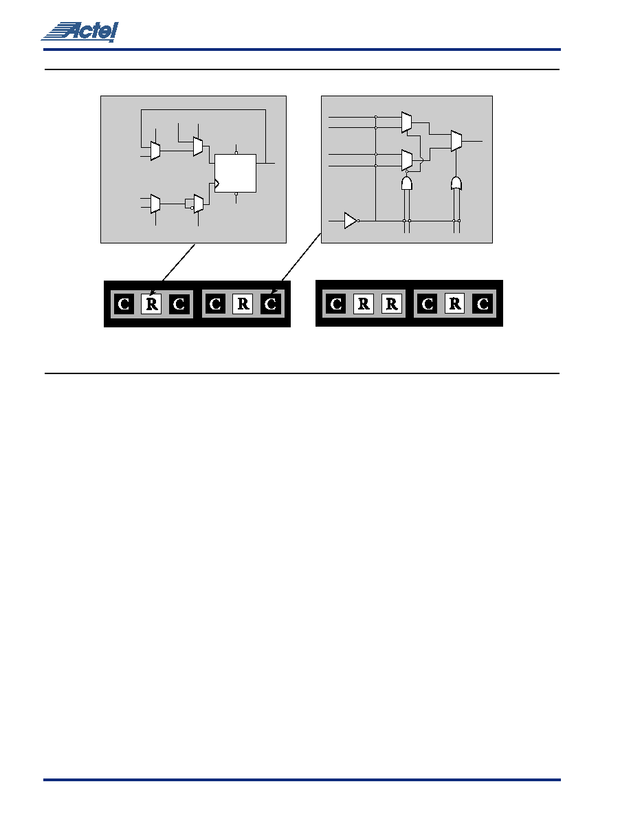
Actel has arranged all C-cell and R-cell logic modules into
horizontal banks called Clusters. There are two types of
Clusters: Type 1 contains two C-cells and one R-cell, while
Type 2 contains one C-cell and two R-cells.
To increase design efficiency and device performance, Actel
has further organized these modules into SuperClusters
(
Figure 4 on page 6
). SuperCluster 1 is a two-wide grouping
of Type 1 clusters. SuperCluster 2 is a two-wide group
containing one Type 1 cluster and one Type 2 cluster. SX
devices feature more SuperCluster 1 modules than
SuperCluster 2 modules because designers typically require
significantly more combinatorial logic than flip-flops.
Figure 2 ∑ R-Cell
Figure 3 ∑ C-Cell
Direct
Connect
Input
CLKA,
CLKB,
Internal Logic
HCLK
CKS
CKP
CLRB
PSETB
Y
D
Q
Routed
Data Input
S0
S1
D0
D1
D2
D3
DB
A0
B0
A1
B1
Sa
Sb
Y
5 4 S X F a m i l y F P G A s
6 v3.1
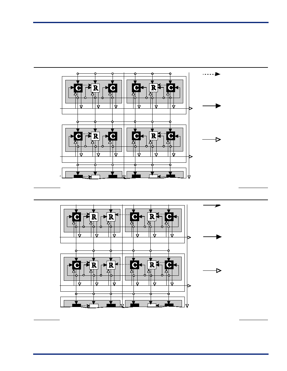
R o u t i n g R e s o u r c e s
Clusters and SuperClusters can be connected through the
use of two innovative local routing resources called
FastConnect and DirectConnect, which enable extremely
fast and predictable interconnection of modules within
Clusters and SuperClusters (
Figure 5
and
Figure 6 on
page 7
). This routing architecture also dramatically reduces
the number of antifuses required to complete a circuit,
ensuring the highest possible performance.
DirectConnect is a horizontal routing resource that provides
connections from a C-cell to its neighboring R-cell in a given
SuperCluster. DirectConnect uses a hard-wired signal path
requiring no programmable interconnection to achieve its
fast signal propagation time of less than 0.1 ns.
FastConnect enables horizontal routing between any two
logic modules within a given SuperCluster and vertical
routing with the SuperCluster immediately below it. Only
one programmable connection is used in a FastConnect
path, delivering maximum pin-to-pin propagation of 0.4 ns.
In addition to DirectConnect and FastConnect, the
architecture makes use of two globally oriented routing
resources known as segmented routing and high-drive
routing. Actel's segmented routing structure provides a
variety of track lengths for extremely fast routing between
SuperClusters. The exact combination of track lengths and
antifuses within each path is chosen by the 100 percent
automatic place and route software to minimize signal
propagation delays.
Actel's high-drive routing structure provides three clock
networks. The first clock, called HCLK, is hard wired from
the HCLK buffer to the clock select MUX in each R-cell. This
provides a fast propagation path for the clock signal,
enabling the 3.7 ns clock-to-out (pin-to-pin) performance of
the SX devices. The hard-wired clock is tuned to provide
clock skew as low as 0.25 ns. The remaining two clocks
(CLKA, CLKB) are global clocks that can be sourced from
external pins or from internal logic signals within the SX
device.
Figure 4 ∑ Cluster Organization
Type 1 SuperCluster
Type 2 SuperCluster
Cluster 1
Cluster 2
Cluster 2
Cluster 1
R-Cell
C-Cell
D0
D1
D2
D3
DB
A0
B0
A1
B1
Sa
Sb
Y
Direct
Connect
Input
CLKA,
CLKB,
Internal Logic
HCLK
CKS
CKP
CLRB
PSETB
Y
D
Q
Routed
Data Input
S0
S1
v3.1
7
5 4 S X F a m i l y F P G A s
O t h e r A r c h i t e c t u r a l F e a t u r e s
Technology
Actel's SX family is implemented on a high-voltage twin-well
CMOS process using 0.35
µ design rules. The metal-to-metal
antifuse is made up of a combination of amorphous silicon
and dielectric material with barrier metals and has a
programmed ("on" state) resistance of 25
with
capacitance of 1.0 fF for low signal impedance.
Figure 5 ∑ DirectConnect and FastConnect for Type 1 SuperClusters
Figure 6 ∑ DirectConnect and FastConnect for Type 2 SuperClusters
Routing Segments
∑ Typically 2 antifuses
∑ Max. 5 antifuses
Fast Connect
∑ One antifuse
∑ 0.4 ns routing delay
Direct Connect
∑ No antifuses
∑ 0.1 ns routing delay
Type 2 SuperClusters
Routing Segments
∑ Typically 2 antifuses
∑ Max. 5 antifuses
Fast Connect
∑ One antifuse
∑ 0.4 ns routing delay
Direct Connect
∑ No antifuses
∑ 0.1 ns routing delay

5 4 S X F a m i l y F P G A s
8 v3.1
P e r f o r m a n c e
The combination of architectural features described above
enables SX devices to operate with internal clock
frequencies exceeding 300 MHz, enabling very fast
execution of even complex logic functions. Thus, the SX
family is an optimal platform upon which to integrate the
functionality previously contained in multiple CPLDs. In
addition, designs that previously would have required a gate
array to meet performance goals can now be integrated into
an SX device with dramatic improvements in cost and time
to market. Using timing-driven place and route tools,
designers can achieve highly deterministic device
performance. With SX devices, designers do not need to use
complicated performance-enhancing design techniques
such as the use of redundant logic to reduce fanout on
critical nets or the instantiation of macros in HDL code to
achieve high performance.
I / O M o d u l e s
Each I/O on an SX device can be configured as an input, an
output, a tristate output, or a bidirectional pin. Even without
the inclusion of dedicated I/O registers, these I/Os, in
combination with array registers, can achieve clock-to-out
(pad-to-pad) timing as fast as 3.7 ns. I/O cells that have
embedded latches and flip-flops require instantiation in
HDL code; this is a design complication not encountered in
SX FPGAs. Fast pin-to-pin timing ensures that the device
will have little trouble interfacing with any other device in
the system, which in turn enables parallel design of system
components and reduces overall design time.
P o w e r R e q u i r e m e n t s
The SX family supports 3.3V operation and is designed to
tolerate 5.0V inputs. (
Table 1
). Power consumption is
extremely low due to the very short distances signals are
required to travel to complete a circuit. Power requirements
are further reduced because of the small number of
low-resistance antifuses in the path. The antifuse
architecture does not require active circuitry to hold a
charge (as do SRAM or EPROM), making it the lowest-power
architecture on the market.
B o u n d a r y S c a n T e s t i n g ( B S T )
All SX devices are IEEE 1149.1 compliant. SX devices offer
superior diagnostic and testing capabilities by providing
Boundary Scan Testing (BST) and probing capabilities.
These functions are controlled through the special test pins
in conjunction with the program fuse. The functionality of
each pin is described in
Table 2
.In the dedicated test mode,
TCK, TDI and TDO are dedicated pins and cannot be used as
regular I/Os. In flexible mode, TMS should be set HIGH
through a pull-up resistor of 10k
. TMS can be pulled LOW
to initiate the test sequence.
The program fuse determines whether the device is in
dedicated or flexible mode. The default (fuse not blown) is
flexible mode. .
D e v e l o p m e n t T o o l S u p p o r t
The SX devices are fully supported by Actel's line of FPGA
development tools, including the Actel DeskTOP series and
Designer Advantage tools. The Actel DeskTOP series is an
integrated design environment for PCs that includes design
entry, simulation, synthesis, and place and route tools.
Designer Advantage, Actel's suite of FPGA development
point tools for PCs and Workstations, includes the ACTgen
Macro Builder, Designer with DirectTime timing driven
place and route and analysis tools, and device programming
software.
In addition, the SX devices contain ActionProbe circuitry
that provides built-in access to every node in a design,
enabling 100-percent real-time observation and analysis of a
device's internal logic nodes without design iteration. The
probe circuitry is accessed by Silicon Explorer II, an
easy-to-use integrated verification and logic analysis tool
that can sample data at 100 MHz (asynchronous) or 66 MHz
(synchronous). Silicon Explorer II attaches to a PC's
standard COM port, turning the PC into a fully functional
18-channel logic analyzer. Silicon Explorer II allows
designers to complete the design verification process at
their desks and reduces verification time from several hours
per cycle to only a few seconds.
Table 1 ∑ Supply Voltages
V
CCA
V
CCI
V
CCR
Maximum
Input
Tolerance
Maximum
Output
Drive
A54SX08
A54SX16
A54SX32
3.3V
3.3V
5.0V
5.0V
3.3V
A54SX16-P
3.3V
3.3V
3.3V
3.3V
3.3V
5.0V
3.3V
5.0V
5.0V
3.3V
5.0V
5.0V
3.3V
3.3V
5.0V
Note:
A54SX16-P has three different entries because it is capable of
both a 3.3V and a 5V drive.
Table 2 ∑ Boundary Scan Pin Functionality
Program Fuse Blown
(Dedicated Test Mode)
Program Fuse Not Blown
(Flexible Mode)
TCK, TDI, TDO are
dedicated BST pins
TCK, TDI, TDO are flexible
and may be used as I/Os
No need for pull-up resistor
for TMS
Use a pull-up resistor of 10k
on TMS
v3.1
9
5 4 S X F a m i l y F P G A s
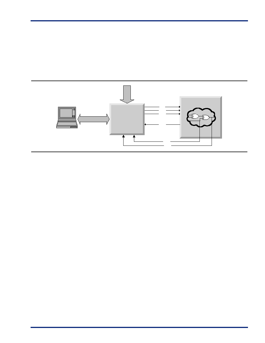
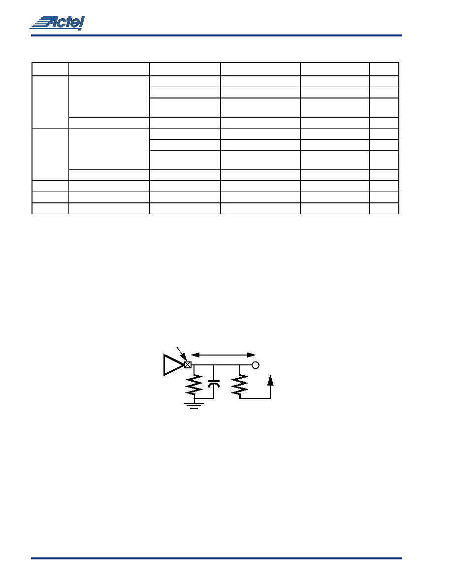
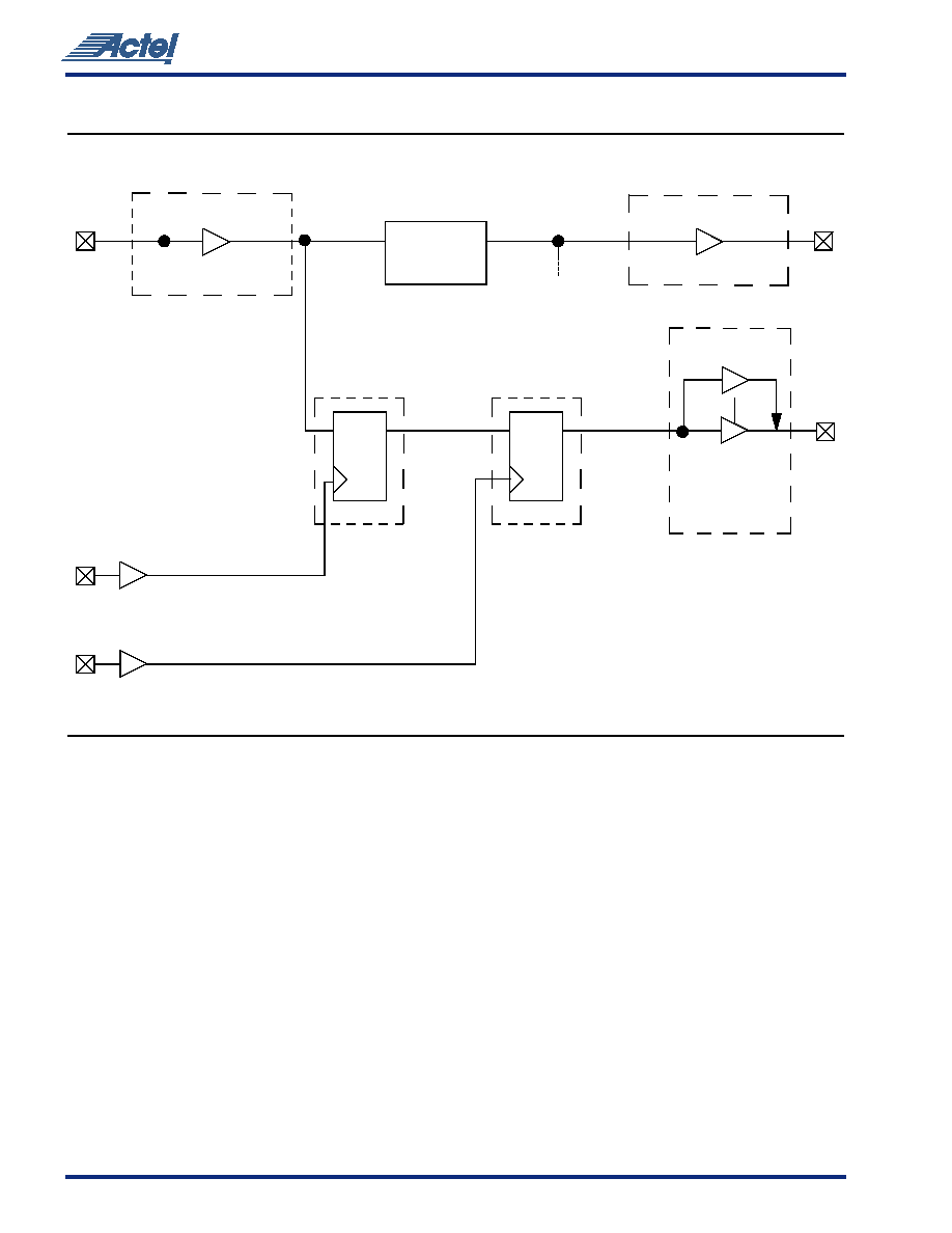
S X P r o b e C i r c u i t C o n t r o l P i n s
The Silicon Explorer II tool uses the boundary scan ports
(TDI, TCK, TMS and TDO) to select the desired nets for
verification. The selected internal nets are assigned to the
PRA/PRB pins for observation.
Figure 7
illustrates the
interconnection between Silicon Explorer II and the FPGA
to perform in-circuit verification. The TRST pin is equipped
with a pull-up resistor. To remove the boundary scan state
machine from the reset state during probing, it is
recommended that the TRST pin be left floating.
D e s i g n C o n s i d e r a t i o n s
The TDI, TCK, TDO, PRA, and PRB pins should not be used
as input or bidirectional ports. Because these pins are
active during probing, critical signals input through these
pins are not available while probing. In addition, the
Security Fuse should not be programmed because doing so
disables the Probe Circuitry.
Figure 7 ∑ Probe Setup
SX FPGA
TDI
TCK
TDO
TMS
PRA
PRB
Serial Connection
16
Channel
Silicon Explorer II

5 4 S X F a m i l y F P G A s
10 v3.1
3 . 3 V / 5 V O p e r a t i n g C o n d i t i o n s
A b s o l u t e M a x i m u m R a t i n g s
1
Symbol
Parameter
Limits
Units
V
CCR
2
DC Supply Voltage
3
≠0.3 to +6.0
V
V
CCA
2
DC Supply Voltage
≠0.3 to +4.0
V
V
CCI
2
DC Supply Voltage
(A54SX08, A54SX16,
A54SX32)
≠0.3 to +4.0
V
V
CCI
2
DC Supply Voltage
(A54SX16P)
≠0.3 to +6.0
V
V
I
Input Voltage
≠0.5 to +5.5
V
V
O
Output Voltage
≠0.5 to +3.6
V
I
IO
I/O Source Sink
Current
3
≠30 to +5.0
mA
T
STG
Storage Temperature
≠65 to +150
∞C
Notes:
1.
Stresses beyond those listed under "Absolute Maximum
Ratings" may cause permanent damage to the device.
Exposure to absolute maximum rated conditions for extended
periods may affect device reliability. Device should not be
operated outside the Recommended Operating Conditions.
2.
V
CCR
in the A54SX16P must be greater than or equal to V
CCI
during power-up and power-down sequences and during
normal operation.
3.
Device inputs are normally high impedance and draw
extremely low current. However, when input voltage is greater
than V
CC
+ 0.5V or less than GND ≠ 0.5V, the internal protection
diodes will forward-bias and can draw excessive current.
R e c o m m e n d e d O p e r a t i n g C o n d i t i o n s
Parameter
Commer
cial
Industrial
Military
Units
Temperature
Range
1
0 to+70
≠40 to +85
≠55 to +125
∞
C
3.3V Power
Supply
Tolerance
±
10
±
10
±
10
%V
C
C
5.0V Power
Supply
Tolerance
±
5
±
10
±
10
%V
C
C
Note:
1.
Ambient temperature (T
A
) is used for commercial and
industrial; case temperature (T
C
) is used for military.
E l e c t r i c a l S p e c i f i c a t i o n s
Commercial
Industrial
Symbol
Parameter
Min.
Max.
Min.
Max.
Units
V
OH
(I
OH
= -20uA) (CMOS)
(I
OH
= -8mA) (TTL)
(I
OH
= -6mA) (TTL)
(V
CCI
≠ 0.1)
2.4
V
CCI
V
CCI
(V
CCI
≠ 0.1)
2.4
V
CCI
V
CCI
V
V
OL
(I
OL
= 20uA) (CMOS)
(I
OL
= 12mA) (TTL)
(I
OL
= 8mA) (TTL)
0.10
0.50
0.50
V
V
IL
0.8
0.8
V
V
IH
2.0
2.0
V
t
R
, t
F
Input Transition Time t
R
, t
F
50
50
ns
C
IO
C
IO
I/O Capacitance
10
10
pF
I
CC
Standby Current, I
CC
4.0
4.0
mA
I
CC(D)
I
CC(D)
I
Dynamic
V
CC
Supply Current
See "Evaluating Power in 54SX Devices" on page 18
v3.1
11
5 4 S X F a m i l y F P G A s
P C I C o m p l i a n c e f o r t h e 5 4 S X F a m i l y
The 54SX family supports 3.3V and 5V PCI and is compliant with the PCI Local Bus Specification Rev. 2.1.
A54SX16P DC Specifications (5.0V PCI Operation)
Symbol
Parameter
Condition
Min.
Max.
Units
V
CCA
Supply Voltage for Array
3.0
3.6
V
V
CCR
Supply Voltage required for Internal Biasing
4.75
5.25
V
V
CCI
Supply Voltage for IOs
4.75
5.25
V
V
IH
Input High Voltage
1
2.0
V
CC
+ 0.5
V
V
IL
Input Low Voltage
1
≠0.5
0.8
V
I
IH
Input High Leakage Current
V
IN
= 2.7
70
µA
I
IL
Input Low Leakage Current
V
IN
= 0.5
≠70
µA
V
OH
Output High Voltage
I
OUT
= ≠2 mA
2.4
V
V
OL
Output Low Voltage
2
I
OUT
= 3 mA, 6 mA
0.55
V
C
IN
Input Pin Capacitance
3
10
pF
C
CLK
CLK Pin Capacitance
5
12
pF
C
IDSEL
IDSEL Pin Capacitance
4
8
pF
Notes:
1.
Input leakage currents include hi-Z output leakage for all bi-directional buffers with tri-state outputs.
2.
Signals without pull-up resistors must have 3 mA low output current. Signals requiring pull up must have 6 mA; the latter include,
FRAME#, IRDY#, TRDY#, DEVSEL#, STOP#, SERR#, PERR#, LOCK#, and, when used AD[63::32], C/BE[7::4]#, PAR64, REQ64#, and ACK64#.
3.
Absolute maximum pin capacitance for a PCI input is 10 pF (except for CLK).
4.
Lower capacitance on this input-only pin allows for non-resistive coupling to AD[xx].
5 4 S X F a m i l y F P G A s
12 v3.1
A54SX16P AC Specifications for (PCI Operation)
Symbol
Parameter
Condition
Min.
Max.
Units
I
OH(AC)
Switching Current High
0 < V
OUT
1.4
1
≠44 mA
1.4
V
OUT
< 2.4
1, 2
≠44 + (V
OUT
≠ 1.4)/0.024
mA
3.1 < V
OUT
< V
CC
1, 3
Equation A: on
page 13
(Test Point)
V
OUT
= 3.1
3
≠142
mA
I
OL(AC)
Switching Current High
V
OUT
2.2
1
95
mA
2.2 > V
OUT
> 0.55
1
V
OUT
/0.023
0.71 > V
OUT
> 0
1, 3
Equation B: on
page 13
mA
(Test Point)
V
OUT
= 0.71
3
206
mA
I
CL
Low Clamp Current
≠5 < V
IN
≠1
≠25 + (V
IN
+ 1)/0.015
mA
slew
R
Output Rise Slew Rate
0.4V to 2.4V load
4
1
5
V/ns
slew
F
Output Fall Slew Rate
2.4V to 0.4V load
4
1
5
V/ns
Notes:
1.
Refer to the V/I curves in
Figure 8
. Switching current characteristics for REQ# and GNT# are permitted to be one half of that specified here;
i.e., half size output drivers may be used on these signals. This specification does not apply to CLK and RST# which are system outputs.
"Switching Current High" specification are not relevant to SERR#, INTA#, INTB#, INTC#, and INTD# which are open drain outputs.
2.
Note that this segment of the minimum current curve is drawn from the AC drive point directly to the DC drive point rather than toward
the voltage rail (as is done in the pull-down curve). This difference is intended to allow for an optional N-channel pull-up.
3.
Maximum current requirements must be met as drivers pull beyond the last step voltage. Equations defining these maximums (A and B)
are provided with the respective diagrams in
Figure 8
. The equation defined maxima should be met by design. In order to facilitate
component testing, a maximum current test point is defined for each side of the output driver.
4.
This parameter is to be interpreted as the cumulative edge rate across the specified range, rather than the instantaneous rate at any point
within the transition range. The specified load (diagram below) is optional; i.e., the designer may elect to meet this parameter with an
unloaded output per revision 2.0 of the PCI Local Bus Specification. However, adherence to both maximum and minimum parameters is
now required (the maximum is no longer simply a guideline). Since adherence to the maximum slew rate was not required prior to
revision 2.1 of the specification, there may be components in the market for some time that have faster edge rates; therefore, motherboard
designers must bear in mind that rise and fall times faster than this specification could occur, and should ensure that signal integrity
modeling accounts for this. Rise slew rate does not apply to open drain outputs.
output
buffer
1/2 in. max.
V
CC
1k
10 pF
1k
pin
v3.1
13
5 4 S X F a m i l y F P G A s
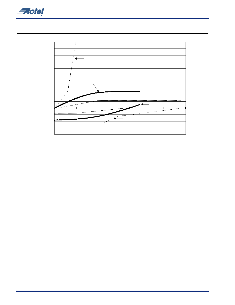
Figure 8
shows the 5.0V PCI V/I curve and the minimum and maximum PCI drive characteristics of the A54SX16P family.
Equation A:
I
OH
= 11.9 * (V
OUT
≠ 5.25) * (V
OUT
+ 2.45)
for V
CC
> V
OUT
> 3.1V
Equation B:
I
OL
= 78.5 * V
OUT
* (4.4 ≠ V
OUT
)
for 0V < V
OUT
< 0.71V
Figure 8 ∑ 5.0V PCI Curve for A54SX16P Family
1
2
3
4
5
6
≠0.20
≠0.15
≠0.10
≠0.05
0
0.05
0.10
0.15
0.20
0.25
0.30
0.35
0.40
0.45
0.50
Voltage Out
Current (A)
SX PCI IOL
SX PCI IOH
PCI IOL Maximum
PCI IOH Maximum
PCI IOH Mininum
PCI IOL Mininum
5 4 S X F a m i l y F P G A s
14 v3.1
A 5 4 S X 1 6 P D C S p e c i f i c a t i o n s ( 3 . 3 V P C I O p e r a t i o n )
Symbol
Parameter
Condition
Min.
Max.
Units
V
CCA
Supply Voltage for Array
3.0
3.6
V
V
CCR
Supply Voltage required for Internal Biasing
3.0
3.6
V
V
CCI
Supply Voltage for IOs
3.0
3.6
V
V
IH
Input High Voltage
0.5V
CC
V
CC
+ 0.5
V
V
IL
Input Low Voltage
≠0.5
0.3V
CC
V
I
IPU
Input Pull-up Voltage
1
0.7V
CC
V
I
IL
Input Leakage Current
2
0 < V
IN
< V
CC
±10
µA
V
OH
Output High Voltage
I
OUT
= ≠500 µA
0.9V
CC
V
V
OL
Output Low Voltage
I
OUT
= 1500 µA
0.1V
CC
V
C
IN
Input Pin Capacitance
3
10
pF
C
CLK
CLK Pin Capacitance
5
12
pF
C
IDSEL
IDSEL Pin Capacitance
4
8
pF
Notes:
1.
This specification should be guaranteed by design. It is the minimum voltage to which pull-up resistors are calculated to pull a floated
network. Applications sensitive to static power utilization should assure that the input buffer is conducting minimum current at this
input voltage.
2.
Input leakage currents include hi-Z output leakage for all bi-directional buffers with tri-state outputs.
3.
Absolute maximum pin capacitance for a PCI input is 10pF (except for CLK).
4.
Lower capacitance on this input-only pin allows for non-resistive coupling to AD[xx].

v3.1
15
5 4 S X F a m i l y F P G A s
A 54SX16P AC Specifications (3.3V PCI Operation)
Symbol Parameter
Condition
Min.
Max.
Units
Switching Current High
0 < V
OUT
0.3V
CC
1
mA
0.3V
CC
V
OUT
< 0.9V
CC
1
≠12V
CC
mA
I
OH(AC)
0.7V
CC
< V
OUT
< V
CC
1, 2
≠17.1 + (V
CC
≠ V
OUT
)
Equation C: on
page 16
(Test Point)
V
OUT
= 0.7V
CC
2
≠32V
CC
mA
Switching Current High
V
CC
> V
OUT
0.6V
CC
1
mA
0.6V
CC
> V
OUT
> 0.1V
CC
1
16V
CC
mA
I
OL(AC)
0.18V
CC
> V
OUT
> 0
1, 2
26.7V
OUT
on page 16
mA
(Test Point)
V
OUT
= 0.18V
CC
2
38V
CC
I
CL
Low Clamp Current
≠3 < V
IN
≠1
≠25 + (V
IN
+ 1)/0.015
mA
I
CH
High Clamp Current
≠3 < V
IN
≠1
25 + (V
IN
≠ V
OUT
≠ 1)/0.015
mA
slew
R
Output Rise Slew Rate
3
0.2V
CC
to 0.6V
CC
load
1
4
V/ns
slew
F
Output Fall Slew Rate
3
0.6V
CC
to 0.2V
CC
load
1
4
V/ns
Notes:
1.
Refer to the V/I curves in
Figure 9
. Switching current characteristics for REQ# and GNT# are permitted to be one half of that specified here;
i.e., half size output drivers may be used on these signals. This specification does not apply to CLK and RST# which are system outputs.
"Switching Current High" specification are not relevant to SERR#, INTA#, INTB#, INTC#, and INTD# which are open drain outputs.
2.
Maximum current requirements must be met as drivers pull beyond the last step voltage. Equations defining these maximums (C and D)
are provided with the respective diagrams in
Figure 9
. The equation defined maxima should be met by design. In order to facilitate
component testing, a maximum current test point is defined for each side of the output driver.
3.
This parameter is to be interpreted as the cumulative edge rate across the specified range, rather than the instantaneous rate at any point
within the transition range. The specified load (diagram below) is optional; i.e., the designer may elect to meet this parameter with an
unloaded output per the latest revision of the PCI Local Bus Specification. However, adherence to both maximum and minimum
parameters is required (the maximum is no longer simply a guideline). Rise slew rate does not apply to open drain outputs.
output
buffer
1/2 in. max.
V
CC
1k
10 pF
1k
pin
5 4 S X F a m i l y F P G A s
16 v3.1
Figure 9
shows the 3.3V PCI V/I curve and the minimum and maximum PCI drive characteristics of the A54SX16P family.
Equation C:
I
OH
= (98.0/V
CC
) * (V
OUT
≠ V
CC
) * (V
OUT
+ 0.4V
CC
)
for V
CC
> V
OUT
> 0.7 V
CC
Equation D:
I
OL
= (256/V
CC
) * V
OUT
* (V
CC
≠ V
OUT
)
for 0V < V
OUT
< 0.18 V
CC
Figure 9 ∑ 3.3V PCI Curve for A54SX16P Family
1
2
3
4
5
6
Voltage Out
≠0.20
≠0.15
≠0.10
≠0.05
0
0.05
0.10
0.15
0.20
0.25
0.30
0.35
0.40
0.45
0.50
Current (A)
SX PCI IOL
SX PCI IOH
PCI IOL Maximum
PCI IOH Maximum
PCI IOH Minimum
PCI IOL Minimum
v3.1
17
5 4 S X F a m i l y F P G A s
P o w e r - U p S e q u e n c i n g
P o w e r - D o w n S e q u e n c i n g
V
CCA
V
CCR
V
CCI
Power-Up Sequence
Comments
A54SX08, A54SX16, A54SX32
3.3V
5.0V
3.3V
5.0V First
3.3V Second
No possible damage to device.
3.3V First
5.0V Second
Possible damage to device.
A54SX16P
3.3V
3.3V
3.3V
3.3V Only
No possible damage to device.
3.3V
5.0V
3.3V
5.0V First
3.3V Second
No possible damage to device.
3.3V First
5.0V Second
Possible damage to device.
3.3V
5.0V
5.0V
5.0V First
3.3V Second
No possible damage to device.
3.3V First
5.0V Second
No possible damage to device.
V
CCA
V
CCR
V
CCI
Power-Down Sequence
Comments
A54SX08, A54SX16, A54SX32
3.3V
5.0V
3.3V
5.0V First
3.3V Second
No possible damage to device.
3.3V First
5.0V Second
Possible damage to device.
A54SX16P
3.3V
3.3V
3.3V
3.3V Only
No possible damage to device.
3.3V
5.0V
3.3V
5.0V First
3.3V Second
Possible damage to device.
3.3V First
5.0V Second
No possible damage to device.
3.3V
5.0V
5.0V
5.0V First
3.3V Second
No possible damage to device.
3.3V First
5.0V Second
No possible damage to device.

5 4 S X F a m i l y F P G A s
18 v3.1
E v a l u a t i n g P o w e r i n 5 4 S X D e v i c e s
A critical element of system reliability is the ability of
electronic devices to safely dissipate the heat generated
during operation. The thermal characteristics of a circuit
depend on the device and package used, the operating
temperature, the operating current, and the system's ability
to dissipate heat.
You should complete a power evaluation early in the design
process to help identify potential heat-related problems in
the system and to prevent the system from exceeding the
device's maximum allowed junction temperature.
The actual power dissipated by most applications is
significantly lower than the power the package can
dissipate. However, a thermal analysis should be performed
for all projects. To perform a power evaluation, follow these
steps:
∑ Estimate the power consumption of the application.
∑ Calculate the maximum power allowed for the device and
package.
∑ Compare the estimated power and maximum power
values.
E s t i m a t i n g P o w e r C o n s u m p t i o n
The total power dissipation for the 54SX family is the sum of
the DC power dissipation and the AC power dissipation. Use
Equation 1 to calculate the estimated power consumption of
your application.
P
Total
= P
DC
+ P
AC
(1)
D C P o w e r D i s s i p a t i o n
The power due to standby current is typically a small
component of the overall power. The Standby power is
shown below for commercial, worst case conditions (70
∞C).
The DC power dissipation is defined in Equation 2 as
follows:
P
DC
= (I
standby
)*V
CCA
+ (I
standby
)*V
CCR
+
(I
standby
)*V
CCI
+ x*V
OL
*I
OL
+ y*(V
CCI
≠ V
OH
)*V
OH
(2)
A C P o w e r D i s s i p a t i o n
The power dissipation of the 54SX Family is usually
dominated by the dynamic power dissipation. Dynamic
power dissipation is a function of frequency, equivalent
capacitance and power supply voltage. The AC power
dissipation is defined as follows:
P
AC
= P
Module
+ P
RCLKA Net
+ P
RCLKB Net
+ P
HCLK Net
+
P
Output Buffer
+ P
Input Buffer
(3)
P
AC
= V
CCA
2
* [(m * C
EQM
* f
m
)
Module
+
(n * C
EQI
* f
n
)
Input Buffer
+ (p * (C
EQO
+ C
L
) * f
p
)
Output Buffer
+
(0.5 * (q
1
* C
EQCR
* f
q1
) + (r
1
* f
q1
))
RCLKA
+
(0.5 * (q
2
* C
EQCR
* f
q2
)+ (r
2
* f
q2
))
RCLKB
+
(0.5 * (s
1
* C
EQHV
* f
s1
) + (C
EQHF
* f
s1
))
HCLK
]
(4)
D e f i n i t i o n o f T e r m s U s e d i n F o r m u l a
Table 3 ∑
I
CC
V
CC
Power
4mA
3.6V
14.4mW
m
= Number of logic modules switching at f
m
n
= Number of input buffers switching at f
n
p
= Number of output buffers switching at f
p
q
1
= Number of clock loads on the first routed array
clock
q
2
= Number of clock loads on the second routed
array clock
x
= Number of I/Os at logic low
y
= Number of I/Os at logic high
r
1
= Fixed capacitance due to first routed array
clock
r
2
= Fixed capacitance due to second routed array
clock
s
1
= Number of clock loads on the dedicated array
clock
C
EQM
= Equivalent capacitance of logic modules in pF
C
EQI
= Equivalent capacitance of input buffers in pF
C
EQO
= Equivalent capacitance of output buffers in pF
C
EQCR
= Equivalent capacitance of routed array clock in
pF
C
EQHV
= Variable capacitance of dedicated array clock
C
EQHF
= Fixed capacitance of dedicated array clock
C
L
= Output lead capacitance in pF
f
m
= Average logic module switching rate in MHz
f
n
= Average input buffer switching rate in MHz
f
p
= Average output buffer switching rate in MHz
f
q1
= Average first routed array clock rate in MHz
f
q2
= Average second routed array clock rate in MHz
f
s1
= Average dedicated array clock rate in MHz
A54SX08 A54SX16 A54SX16P A54SX32
C
EQM
(pF) 4.0
4.0
4.0
4.0
C
EQI
(pF) 3.4
3.4
3.4
3.4
C
EQO
(pF) 4.7
4.7
4.7
4.7
C
EQCR
(pF) 1.6
1.6
1.6
1.6
C
EQHV
0.615
0.615
0.615
0.615
C
EQHF
60
96
96
140
r
1
(pF)
87
138
138
171
r
2
(pF)
87
138
138
171

v3.1
19
5 4 S X F a m i l y F P G A s
G u i d e l i n e s f o r C a l c u l a t i n g P o w e r
C o n s u m p t i o n
The following guidelines are meant to represent worst-case
scenarios so that they can be generally used to predict the
upper limits of power dissipation. These guidelines are as
follow:
S a m p l e P o w e r C a l c u l a t i o n
One of the designs used to characterize the A54SX family
was a 528 bit serial in serial out shift register. The design
utilized 100% of the dedicated flip-flops of an A54SX16P
device. A pattern of 0101... was clocked into the device at
frequencies ranging from 1 MHz to 200 MHz. Shifting in a
series of 0101... caused 50% of the flip-flops to toggle from
low to high at every clock cycle.
Follow the steps below to estimate power consumption. The
values provided for the sample calculation below are for the
shift register design above. This method for estimating
power consumption is conservative and the actual power
consumption of your design may be less than the estimated
power consumption.
The total power dissipation for the 54SX family is the sum of
the AC power dissipation and the DC power dissipation.
P
Total
= P
AC
(dynamic power) + P
DC
(static power)
(5)
A C P o w e r D i s s i p a t i o n
P
AC
= P
Module
+ P
RCLKA Net
+ P
RCLKB Net
+ P
HCLK Net
+
P
Output Buffer
+ P
Input Buffer
(6)
P
AC
= V
CCA
2
* [(m * C
EQM
* f
m
)
Module
+
(n * C
EQI
* f
n
)
Input Buffer
+ (p * (C
EQO
+ C
L
) * f
p
)
Output
Buffer
+
(0.5 * (q
1
* C
EQCR
* f
q1
) + (r
1
* f
q1
))
RCLKA
+
(0.5 * (q
2
* C
EQCR
* f
q2
)+ (r
2
* f
q2
))
RCLKB
+
(0.5 * (s
1
* C
EQHV
* f
s1
) + (C
EQHF
* f
s1
))
HCLK
]
(7)
Step #1:
Define Terms Used in Formula
Logic Modules (m)
= 20% of modules
Inputs Switching (n)
= # inputs/4
Outputs Switching (p)
= # output/4
First Routed Array Clock Loads (q
1
)
= 20% of register
cells
Second Routed Array Clock Loads (q
2
) = 20% of register
cells
Load Capacitance (C
L
)
= 35 pF
Average Logic Module Switching Rate
(f
m
)
= f/10
Average Input Switching Rate (f
n
)
= f/5
Average Output Switching Rate (f
p
)
= f/10
Average First Routed Array Clock Rate
(f
q1
)
= f/2
Average Second Routed Array Clock
Rate (f
q2
)
= f/2
Average Dedicated Array Clock Rate
(f
s1
)
= f
Dedicated Clock Array clock loads (s
1
) = 20% of regular
modules
V
CCA
3.3
Module
Number of logic modules switching at f
m
(Used 50%)
m
264
Average logic modules switching rate
f
m
(MHz) (Guidelines: f/10)
f
m
20
Module capacitance C
EQM
(pF)
C
EQM
4.0
Input Buffer
Number of input buffers switching at f
n
n
1
Average input switching rate f
n
(MHz)
(Guidelines: f/5)
f
n
40
Input buffer capacitance C
EQI
(pF)
C
EQI
3.4
Output Buffer
Number of output buffers switching at f
p
p
1
Average output buffers switching rate
f
p
(MHz) (Guidelines: f/10)
f
p
20
Output buffers buffer Capacitance C
EQO
(pF) C
EQO
4.7
Output Load capacitance C
L
(pF)
C
L
35
RCLKA
Number of Clock loads q
1
q
1
528
Capacitance of routed array clock (pF)
C
EQCR
1.6
Average clock rate (MHz)
f
q1
200
Fixed capacitance (pF)
r
1
138
RCLKB
Number of Clock loads q
2
q
2
0
Capacitance of routed array clock (pF)
C
EQCR
1.6
Average clock rate (MHz)
f
q2
0
Fixed capacitance (pF)
r
2
138
HCLK
Number of Clock loads
s
1
0
Variable capacitance of dedicated
array clock (pF)
C
EQHV
0.615
Fixed capacitance of dedicated
array clock (pF)
C
EQHF
96
Average clock rate (MHz)
f
s1
0
5 4 S X F a m i l y F P G A s
20 v3.1
Step #2:
Calculate Dynamic Power Consumption
Step #3:
Calculate DC Power Dissipation
DC Power Dissipation
P
DC
= (I
standby
)*V
CCA
+ (I
standby
)*V
CCR
+ (I
standby
)*V
CCI
+
X*V
OL
*I
OL
+ Y*(V
CCI
≠ V
OH
)*V
OH
(8)
For a rough estimate of DC Power Dissipation, only use
P
DC
= (I
standby
)*V
CCA
. The rest of the formula provides a
very small number that can be considered negligible.
P
DC
= (I
standby
)*V
CCA
P
DC
= .55mA*3.3V
P
DC
= 0.001815W
Step #4:
Calculate Total Power Consumption
P
Total
= P
AC
+ P
DC
P
Total
= 1.461 + 0.001815
P
Total
= 1.4628W
Step #5:
Compare Estimated Power Consumption against
Characterized Power Consumption
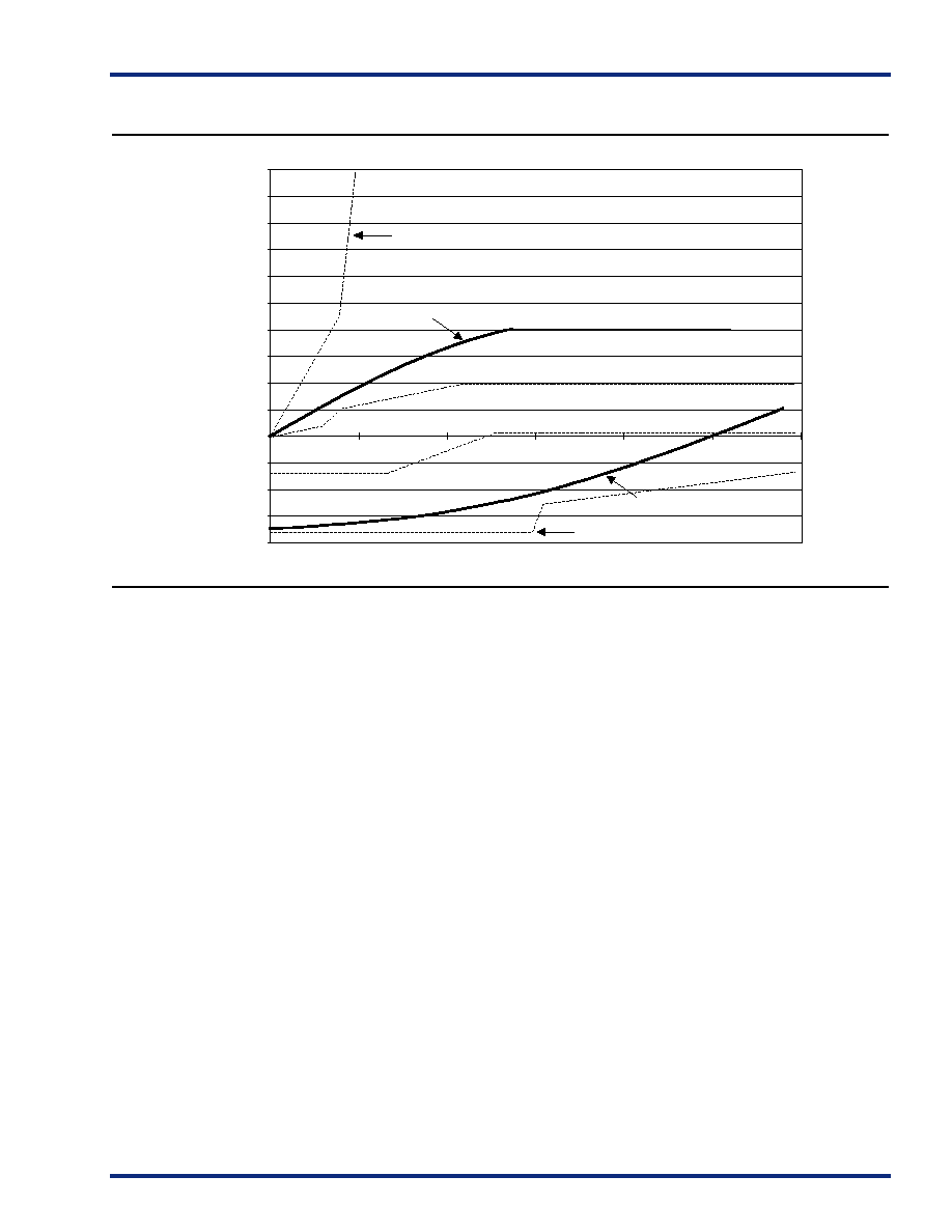
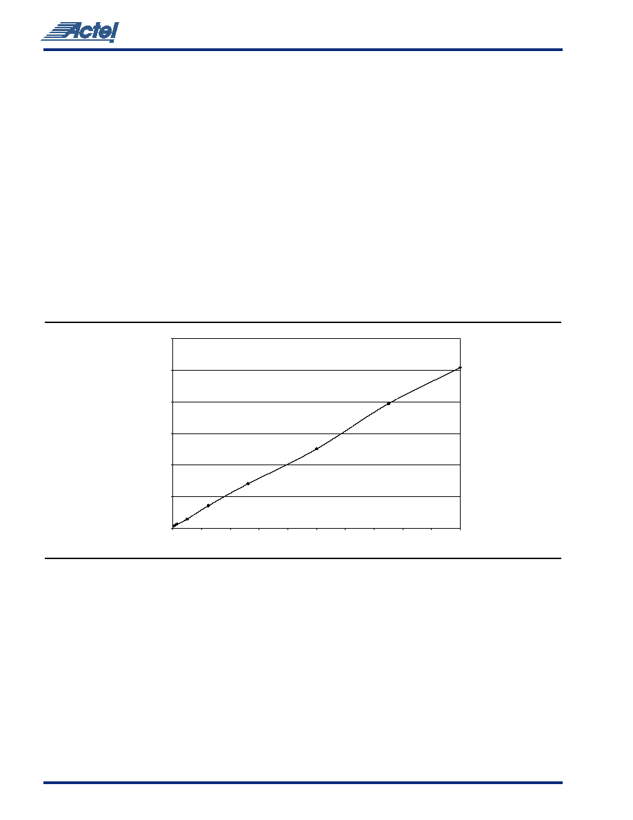
The estimated total power consumption for this design is
1.46W. The characterized power consumption for this design
at 200 MHz is 1.0164W.
Figure 10
shows the characterized
power dissipation numbers for the shift register design
using frequencies ranging from 1 MHz to 200 MHz.
V
CCA
*V
CCA
10.89
m*f
m
*C
EQM
0.02112
n*f
n
*C
EQI
0.000136
p*f
p
*(C
EQO
+C
L
)
0.000794
0.5*(q
1
*C
EQCR
*f
q1
)+(r
1
*f
q1
)
0.11208
0.5*(q
2
*C
EQCR
*f
q2
)+(r
2
*f
q2
)
0
0.5 *(s
1
* C
EQHV
* f
s1
)+(C
EQHF
*f
s1
)
0
P
AC
= 1.461W
Figure 10 ∑ Power Dissipation
0
200
400
600
800
1000
1200
Frequency MHz
Power Dissipation mW
20
0
40
60
80
100
120
140
160
180
200
v3.1
21
5 4 S X F a m i l y F P G A s
J u n c t i o n T e m p e r a t u r e ( T
J
)
The temperature that you select in Designer Series software
is the junction temperature, not ambient temperature. This
is an important distinction because the heat generated from
dynamic power consumption is usually hotter than the
ambient temperature. Use the equation below to calculate
junction temperature.
Junction Temperature =
T + T
a
Where:
T
a
= Ambient Temperature
T = Temperature gradient between junction (silicon) and
ambient
T =
ja
* P
P = Power calculated from Estimating Power Consumption
section
ja
= Junction to ambient of package.
ja
numbers are
located in Package Thermal Characteristics section.
P a c k a g e T h e r m a l C h a r a c t e r i s t i c s
The device junction to case thermal characteristic is
jc
,
and the junction to ambient air characteristic is
ja
. The
thermal characteristics for
ja
are shown with two different
air flow rates.
The maximum junction temperature is 150
∞C.
A sample calculation of the absolute maximum power
dissipation allowed for a TQFP 176-pin package at
commercial temperature and still air is as follows:
Package Type
Pin Count
jc
ja
Still Air
ja
300 ft/min
Units
Plastic Leaded Chip Carrier (PLCC)
84
12
32
22
∞
C/W
Thin Quad Flat Pack (TQFP)
144
11
32
24
∞
C/W
Thin Quad Flat Pack (TQFP)
176
11
28
21
∞
C/W
Very Thin Quad Flatpack (VQFP)
100
10
38
32
∞
C/W
Plastic Quad Flat Pack (PQFP) without Heat Spreader
208
8
30
23
∞
C/W
Plastic Quad Flat Pack (PQFP) with Heat Spreader
208
3.8
20
17
∞
C/W
Plastic Ball Grid Array (PBGA)
272
3
20
14.5
∞
C/W
Plastic Ball Grid Array (PBGA)
313
3
23
17
∞
C/W
Plastic Ball Grid Array (PBGA)
329
3
18
13.5
∞
C/W
Fine Pitch Ball Grid Array (FBGA)
144
3.8
38.8
26.7
∞
C/W
Note:
SX08 does not have a heat spreader.
Maximum Power Allowed
Max. junction temp. (∞C) ≠ Max. ambient temp. (∞C)
ja
(∞C/W)
------------------------------------------------------------------------------------------------------------------------------
150∞C ≠ 70∞C
28∞C/W
---------------------------------
2.86W
=
=
=
5 4 S X F a m i l y F P G A s
22 v3.1
5 4 S X T i m i n g M o d e l *
H a r d - W i r e d C l o c k
External Set-Up
= t
INY
+ t
IRD1
+ t
SUD
≠ t
HCKH
= 1.5 + 0.3 + 0.5 ≠ 1.0 = 1.3 ns
Clock-to-Out (Pin-to-Pin)
= t
HCKH
+ t
RCO
+ t
RD1
+ t
DHL
= 1.0 + 0.8 + 0.3 + 1.6 = 3.7 ns
R o u t e d C l o c k
External Set-Up = t
INY
+ t
IRD1
+ t
SUD
≠ t
RCKH
= 1.5 + 0.3 + 0.5 ≠ 1.5 = 0.8 ns
Clock-to-Out (Pin-to-Pin)
= t
RCKH
+ t
RCO
+ t
RD1
+ t
DHL
= 1.52+ 0.8 + 0.3 + 1.6 = 4.2 ns
*Values shown for A54SX08-3, worst-case commercial conditions.
Output Delays
Internal Delays
Input Delays
Hard-Wired
I/O Module
F
HMAX
= 320 MHz
t
INY
= 1.5 ns
t
IRD2
= 0.6 ns
Combinatorial
Cell
t
PD
=0.6 ns
Register
Cell
I/O Module
t
RD1
= 0.3 ns
t
DHL
= 1.6 ns
I/O Module
Routed
Clock
F
MAX
= 250 MHz
D
Q
D
Q
t
DHL
= 1.6 ns
t
ENZH
= 2.3 ns
t
RD1
= 0.3 ns
t
RCO
= 0.8 ns
t
SUD
= 0.5 ns
t
HD
= 0.0 ns
t
RD4
= 1.0 ns
t
RD8
= 1.9 ns
Predicted
Routing
Delays
t
RCKH
= 1.5 ns (100% Load)
t
RD1
= 0.3 ns
Register
Cell
t
RCO
= 0.8 ns
Clock
t
HCKH
= 1.0 ns
v3.1
23
5 4 S X F a m i l y F P G A s
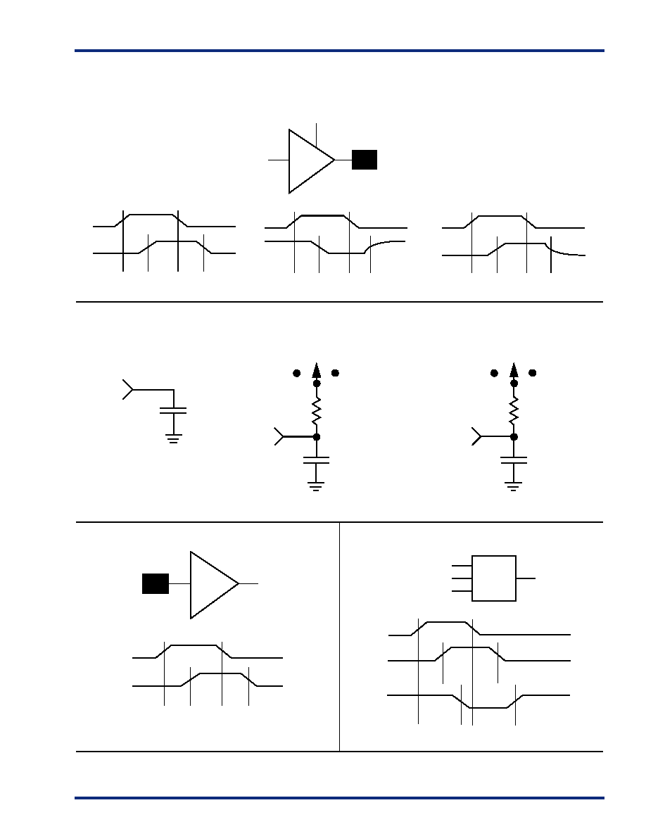
O u t p u t B u f f e r D e l a y s
A C T e s t L o a d s
I n p u t B u f f e r D e l a y s
C - C e l l D e l a y s
To AC test loads (shown below)
PAD
D
E
TRIBUFF
In
V
CC
GND
50%
Out
V
OL
V
OH
1.5V
t
DLH
50%
1.5V
t
DHL
En
V
CC
GND
50%
Out
V
OL
1.5V
t
ENZL
50%
10%
t
ENLZ
En
V
CC
GND
50%
Out
GND
V
OH
1.5V
t
ENZH
50%
90%
t
ENHZ
V
CC
Load 1
(Used to measure
Load 2
(Used to measure enable delays)
35 pF
To the output
V
CC
GND
35 pF
To the output
R to V
CC
for t
PZL
R to GND for t
PZH
R = 1 k
propagation delay)
under test
under test
Load 3
(Used to measure disable delays)
V
CC
GND
5 pF
To the output
R to V
CC
for t
PLZ
R to GND for t
PHZ
R = 1 k
under test
PAD
Y
INBUF
In
3V
0V
1.5V
Out
GND
V
CC
50%
t
INY
1.5V
50%
t
INY
S
A
B
Y
S, A or B
Out
GND
V
CC
50%
t
PD
Out
GND
GND
V
CC
50%
50%
50%
V
CC
50%
50%
t
PD
t
PD
t
PD

5 4 S X F a m i l y F P G A s
24 v3.1
T i m i n g C h a r a c t e r i s t i c s
Timing characteristics for 54SX devices fall into three
categories: family-dependent, device-dependent, and
design-dependent. The input and output buffer
characteristics are common to all 54SX family members.
Internal routing delays are device dependent. Design
dependency means actual delays are not determined until
after placement and routing of the user's design is complete.
Delay values may then be determined by using the
DirectTime Analyzer utility or performing simulation with
post-layout delays.
C r i t i c a l N e t s a n d T y p i c a l N e t s
Propagation delays are expressed only for typical nets,
which are used for initial design performance evaluation.
Critical net delays can then be applied to the most
time-critical paths. Critical nets are determined by net
property assignment prior to placement and routing. Up to
6% of the nets in a design may be designated as critical,
while 90% of the nets in a design are typical.
L o n g T r a c k s
Some nets in the design use long tracks. Long tracks are
special routing resources that span multiple rows, columns,
or modules. Long tracks employ three and sometimes five
antifuse connections. This increases capacitance and
resistance, resulting in longer net delays for macros
connected to long tracks. Typically up to 6% of nets in a fully
utilized device require long tracks. Long tracks contribute
approximately 4 ns to 8.4 ns delay. This additional delay is
represented statistically in higher fanout (FO=24) routing
delays in the data sheet specifications section.
T i m i n g D e r a t i n g
54SX devices are manufactured in a CMOS process.
Therefore, device performance varies according to
temperature, voltage, and process variations. Minimum
timing parameters reflect maximum operating voltage,
minimum operating temperature, and best-case processing.
Maximum timing parameters reflect minimum operating
voltage, maximum operating temperature, and worst-case
processing.
T e m p e r a t u r e a n d V o l t a g e D e r a t i n g F a c t o r s
(Normalized to Worst-Case Commercial, T
J
= 70
∞C, V
CCA
= 3.0V)
R e g i s t e r C e l l T i m i n g C h a r a c t e r i s t i c s
F l i p - F l o p s
(Positive edge triggered)
D
CLK
CLR
Q
D
CLK
Q
CLR
t
HPWH
,
t
WASYN
t
HD
t
SUD
t
HP
t
HPWL
,
t
RCO
t
CLR
t
RPWL
t
RPWH
PRESET
t
PRESET
PRESET
V
CCA
Junction Temperature (T
J
)
≠55
≠40
0
25
70
85
125
3.0
0.75
0.78
0.87
0.89
1.00
1.04
1.16
3.3
0.70
0.73
0.82
0.83
0.93
0.97
1.08
3.6
0.66
0.69
0.77
0.78
0.87
0.92
1.02

v3.1
25
5 4 S X F a m i l y F P G A s
A 5 4 S X 0 8 T i m i n g C h a r a c t e r i s t i c s
(Worst-Case Commercial Conditions, V
CCR
= 4.75V, V
CCA,
V
CCI
= 3.0V, T
J
= 70
∞C)
`≠3' Speed
`≠2' Speed
`≠1' Speed
`Std' Speed
Parameter
Description
Min.
Max.
Min.
Max.
Min.
Max.
Min.
Max.
Units
C-Cell Propagation Delays
1
t
PD
Internal Array Module
0.6
0.7
0.8
0.9
ns
Predicted Routing Delays
2
t
DC
FO=1 Routing Delay, Direct
Connect
0.1
0.1
0.1
0.1
ns
t
FC
FO=1 Routing Delay, Fast Connect
0.3
0.4
0.4
0.5
ns
t
RD1
FO=1 Routing Delay
0.3
0.4
0.4
0.5
ns
t
RD2
FO=2 Routing Delay
0.6
0.7
0.8
0.9
ns
t
RD3
FO=3 Routing Delay
0.8
0.9
1.0
1.2
ns
t
RD4
FO=4 Routing Delay
1.0
1.2
1.4
1.6
ns
t
RD8
FO=8 Routing Delay
1.9
2.2
2.5
2.9
ns
t
RD12
FO=12 Routing Delay
2.8
3.2
3.7
4.3
ns
R-Cell Timing
t
RCO
Sequential Clock-to-Q
0.8
1.1
1.2
1.4
ns
t
CLR
Asynchronous Clear-to-Q
0.5
0.6
0.7
0.8
ns
t
PRESET
Asynchronous Preset-to-Q
0.7
0.8
0.9
1.0
ns
t
SUD
Flip-Flop Data Input Set-Up
0.5
0.5
0.7
0.8
ns
t
HD
Flip-Flop Data Input Hold
0.0
0.0
0.0
0.0
ns
t
WASYN
Asynchronous Pulse Width
1.4
1.6
1.8
2.1
ns
Input Module Propagation Delays
t
INYH
Input Data Pad-to-Y HIGH
1.5
1.7
1.9
2.2
ns
t
INYL
Input Data Pad-to-Y LOW
1.5
1.7
1.9
2.2
ns
Input Module Predicted Routing Delays
2
t
IRD1
FO=1 Routing Delay
0.3
0.4
0.4
0.5
ns
t
IRD2
FO=2 Routing Delay
0.6
0.7
0.8
0.9
ns
t
IRD3
FO=3 Routing Delay
0.8
0.9
1.0
1.2
ns
t
IRD4
FO=4 Routing Delay
1.0
1.2
1.4
1.6
ns
t
IRD8
FO=8 Routing Delay
1.9
2.2
2.5
2.9
ns
t
IRD12
FO=12 Routing Delay
2.8
3.2
3.7
4.3
ns
Notes:
1.
For dual-module macros, use t
PD
+ t
RD1
+ t
PDn
, t
RCO
+ t
RD1
+ t
PDn
or t
PD1
+ t
RD1
+ t
SUD
, whichever is appropriate.
2.
Routing delays are for typical designs across worst-case operating conditions. These parameters should be used for estimating device
performance. Post-route timing analysis or simulation is required to determine actual worst-case performance. Post-route timing is
based on actual routing delay measurements performed on the device prior to shipment.
5 4 S X F a m i l y F P G A s
26 v3.1
A 5 4 S X 0 8 T i m i n g C h a r a c t e r i s t i c s
(continued)
(Worst-Case Commercial Conditions)
`≠3' Speed
`≠2' Speed
`≠1' Speed
`Std' Speed
Parameter
Description
Min.
Max.
Min.
Max.
Min.
Max.
Min.
Max.
Units
Dedicated (Hard-Wired) Array Clock Network
t
HCKH
Input LOW to HIGH
(Pad to R-Cell Input)
1.0
1.1
1.3
1.5
ns
t
HCKL
Input HIGH to LOW
(Pad to R-Cell Input)
1.0
1.2
1.4
1.6
ns
t
HPWH
Minimum Pulse Width HIGH
1.4
1.6
1.8
2.1
ns
t
HPWL
Minimum Pulse Width LOW
1.4
1.6
1.8
2.1
ns
t
HCKSW
Maximum Skew
0.1
0.2
0.2
0.2
ns
t
HP
Minimum Period
2.7
3.1
3.6
4.2
ns
f
HMAX
Maximum Frequency
350
320
280
240
MHz
Routed Array Clock Networks
t
RCKH
Input LOW to HIGH (Light Load)
(Pad to R-Cell Input)
1.3
1.5
1.7
2.0
ns
t
RCKL
Input HIGH to LOW (Light Load)
(Pad to R-Cell Input)
1.4
1.6
1.8
2.1
ns
t
RCKH
Input LOW to HIGH (50% Load)
(Pad to R-Cell Input)
1.4
1.7
1.9
2.2
ns
t
RCKL
Input HIGH to LOW (50% Load)
(Pad to R-Cell Input)
1.5
1.7
2.0
2.3
ns
t
RCKH
Input LOW to HIGH (100% Load)
(Pad to R-Cell Input)
1.5
1.7
1.9
2.2
ns
t
RCKL
Input HIGH to LOW (100% Load)
(Pad to R-Cell Input)
1.5
1.8
2.0
2.3
ns
t
RPWH
Min. Pulse Width HIGH
2.1
2.4
2.7
3.2
ns
t
RPWL
Min. Pulse Width LOW
2.1
2.4
2.7
3.2
ns
t
RCKSW
Maximum Skew (Light Load)
0.1
0.2
0.2
0.2
ns
t
RCKSW
Maximum Skew (50% Load)
0.3
0.3
0.4
0.4
ns
t
RCKSW
Maximum Skew (100% Load)
0.3
0.3
0.4
0.4
ns
TTL Output Module Timing
1
t
DLH
Data-to-Pad LOW to HIGH
1.6
1.9
2.1
2.5
ns
t
DHL
Data-to-Pad HIGH to LOW
1.6
1.9
2.1
2.5
ns
t
ENZL
Enable-to-Pad, Z to L
2.1
2.4
2.8
3.2
ns
t
ENZH
Enable-to-Pad, Z to H
2.3
2.7
3.1
3.6
ns
t
ENLZ
Enable-to-Pad, L to Z
1.4
1.7
1.9
2.2
ns
t
ENHZ
Enable-to-Pad, H to Z
1.3
1.5
1.7
2.0
ns
Note:
1.
Delays based on 35 pF loading, except t
ENZL
and t
ENZH
. For t
ENZL
and t
ENZH
the loading is 5 pF.

v3.1
27
5 4 S X F a m i l y F P G A s
A 5 4 S X 1 6 T i m i n g C h a r a c t e r i s t i c s
(Worst-Case Commercial Conditions, V
CCR
= 4.75V, V
CCA,
V
CCI
= 3.0V, T
J
= 70
∞C)
`≠3' Speed
`≠2' Speed
`≠1' Speed
`Std' Speed
Parameter
Description
Min.
Max.
Min.
Max.
Min.
Max.
Min.
Max.
Units
C-Cell Propagation Delays
1
t
PD
Internal Array Module
0.6
0.7
0.8
0.9
ns
Predicted Routing Delays
2
t
DC
FO=1 Routing Delay, Direct
Connect
0.1
0.1
0.1
0.1
ns
t
FC
FO=1 Routing Delay, Fast Connect
0.3
0.4
0.4
0.5
ns
t
RD1
FO=1 Routing Delay
0.3
0.4
0.4
0.5
ns
t
RD2
FO=2 Routing Delay
0.6
0.7
0.8
0.9
ns
t
RD3
FO=3 Routing Delay
0.8
0.9
1.0
1.2
ns
t
RD4
FO=4 Routing Delay
1.0
1.2
1.4
1.6
ns
t
RD8
FO=8 Routing Delay
1.9
2.2
2.5
2.9
ns
t
RD12
FO=12 Routing Delay
2.8
3.2
3.7
4.3
ns
R-Cell Timing
t
RCO
Sequential Clock-to-Q
0.8
1.1
1.2
1.4
ns
t
CLR
Asynchronous Clear-to-Q
0.5
0.6
0.7
0.8
ns
t
PRESET
Asynchronous Preset-to-Q
0.7
0.8
0.9
1.0
ns
t
SUD
Flip-Flop Data Input Set-Up
0.5
0.5
0.7
0.8
ns
t
HD
Flip-Flop Data Input Hold
0.0
0.0
0.0
0.0
ns
t
WASYN
Asynchronous Pulse Width
1.4
1.6
1.8
2.1
ns
Input Module Propagation Delays
t
INYH
Input Data Pad-to-Y HIGH
1.5
1.7
1.9
2.2
ns
t
INYL
Input Data Pad-to-Y LOW
1.5
1.7
1.9
2.2
ns
Predicted Input Routing Delays
2
t
IRD1
FO=1 Routing Delay
0.3
0.4
0.4
0.5
ns
t
IRD2
FO=2 Routing Delay
0.6
0.7
0.8
0.9
ns
t
IRD3
FO=3 Routing Delay
0.8
0.9
1.0
1.2
ns
t
IRD4
FO=4 Routing Delay
1.0
1.2
1.4
1.6
ns
t
IRD8
FO=8 Routing Delay
1.9
2.2
2.5
2.9
ns
t
IRD12
FO=12 Routing Delay
2.8
3.2
3.7
4.3
ns
Notes:
1.
For dual-module macros, use t
PD
+ t
RD1
+ t
PDn
, t
RCO
+ t
RD1
+ t
PDn
or t
PD1
+ t
RD1
+ t
SUD
, whichever is appropriate.
2.
Routing delays are for typical designs across worst-case operating conditions. These parameters should be used for estimating device
performance. Post-route timing analysis or simulation is required to determine actual worst-case performance. Post-route timing is
based on actual routing delay measurements performed on the device prior to shipment.
5 4 S X F a m i l y F P G A s
28 v3.1
A 5 4 S X 1 6 T i m i n g C h a r a c t e r i s t i c s
(continued)
(Worst-Case Commercial Conditions)
`≠3' Speed
`≠2' Speed
`≠1' Speed
`Std' Speed
Parameter
Description
Min.
Max.
Min.
Max.
Min.
Max.
Min.
Max.
Units
Dedicated (Hard-Wired) Array Clock Network
t
HCKH
Input LOW to HIGH
(Pad to R-Cell Input)
1.2
1.4
1.5
1.8
ns
t
HCKL
Input HIGH to LOW
(Pad to R-Cell Input)
1.2
1.4
1.6
1.9
ns
t
HPWH
Minimum Pulse Width HIGH
1.4
1.6
1.8
2.1
ns
t
HPWL
Minimum Pulse Width LOW
1.4
1.6
1.8
2.1
ns
t
HCKSW
Maximum Skew
0.2
0.2
0.3
0.3
ns
t
HP
Minimum Period
2.7
3.1
3.6
4.2
ns
f
HMAX
Maximum Frequency
350
320
280
240
MHz
Routed Array Clock Networks
t
RCKH
Input LOW to HIGH (Light Load)
(Pad to R-Cell Input)
1.6
1.8
2.1
2.5
ns
t
RCKL
Input HIGH to LOW (Light Load)
(Pad to R-Cell Input)
1.8
2.0
2.3
2.7
ns
t
RCKH
Input LOW to HIGH (50% Load)
(Pad to R-Cell Input)
1.8
2.1
2.5
2.8
ns
t
RCKL
Input HIGH to LOW (50% Load)
(Pad to R-Cell Input)
2.0
2.2
2.5
3.0
ns
t
RCKH
Input LOW to HIGH (100% Load)
(Pad to R-Cell Input)
1.8
2.1
2.4
2.8
ns
t
RCKL
Input HIGH to LOW (100% Load)
(Pad to R-Cell Input)
2.0
2.2
2.5
3.0
ns
t
RPWH
Min. Pulse Width HIGH
2.1
2.4
2.7
3.2
ns
t
RPWL
Min. Pulse Width LOW
2.1
2.4
2.7
3.2
ns
t
RCKSW
Maximum Skew (Light Load)
0.5
0.5
0.5
0.7
ns
t
RCKSW
Maximum Skew (50% Load)
0.5
0.6
0.7
0.8
ns
t
RCKSW
Maximum Skew (100% Load)
0.5
0.6
0.7
0.8
ns
TTL Output ModuleTiming
1
t
DLH
Data-to-Pad LOW to HIGH
1.6
1.9
2.1
2.5
ns
t
DHL
Data-to-Pad HIGH to LOW
1.6
1.9
2.1
2.5
ns
t
ENZL
Enable-to-Pad, Z to L
2.1
2.4
2.8
3.2
ns
t
ENZH
Enable-to-Pad, Z to H
2.3
2.7
3.1
3.6
ns
t
ENLZ
Enable-to-Pad, L to Z
1.4
1.7
1.9
2.2
ns
t
ENHZ
Enable-to-Pad, H to Z
1.3
1.5
1.7
2.0
ns
Note:
1.
Delays based on 35 pF loading, except t
ENZL
and t
ENZH
. For t
ENZL
and t
ENZH
the loading is 5 pF.
v3.1
29
5 4 S X F a m i l y F P G A s
A 5 4 S X 1 6 P T i m i n g C h a r a c t e r i s t i c s
(Worst-Case Commercial Conditions, V
CCR
= 4.75V, V
CCA,
V
CCI
= 3.0V, T
J
= 70
∞C)
`≠3' Speed
`≠2' Speed
`≠1' Speed
`Std' Speed
Parameter
Description
Min.
Max.
Min.
Max.
Min.
Max.
Min.
Max.
Units
C-Cell Propagation Delays
1
t
PD
Internal Array Module
0.6
0.7
0.8
0.9
ns
Predicted Routing Delays
2
t
DC
FO=1 Routing Delay, Direct
Connect
0.1
0.1
0.1
0.1
ns
t
FC
FO=1 Routing Delay, Fast Connect
0.3
0.4
0.4
0.5
ns
t
RD1
FO=1 Routing Delay
0.3
0.4
0.4
0.5
ns
t
RD2
FO=2 Routing Delay
0.6
0.7
0.8
0.9
ns
t
RD3
FO=3 Routing Delay
0.8
0.9
1.0
1.2
ns
t
RD4
FO=4 Routing Delay
1.0
1.2
1.4
1.6
ns
t
RD8
FO=8 Routing Delay
1.9
2.2
2.5
2.9
ns
t
RD12
FO=12 Routing Delay
2.8
3.2
3.7
4.3
ns
R-Cell Timing
t
RCO
Sequential Clock-to-Q
0.9
1.1
1.3
1.4
ns
t
CLR
Asynchronous Clear-to-Q
0.5
0.6
0.7
0.8
ns
t
PRESET
Asynchronous Preset-to-Q
0.7
0.8
0.9
1.0
ns
t
SUD
Flip-Flop Data Input Set-Up
0.5
0.5
0.7
0.8
ns
t
HD
Flip-Flop Data Input Hold
0.0
0.0
0.0
0.0
ns
t
WASYN
Asynchronous Pulse Width
1.4
1.6
1.8
2.1
ns
Input Module Propagation Delays
t
INYH
Input Data Pad-to-Y HIGH
1.5
1.7
1.9
2.2
ns
t
INYL
Input Data Pad-to-Y LOW
1.5
1.7
1.9
2.2
ns
Predicted Input Routing Delays
2
t
IRD1
FO=1 Routing Delay
0.3
0.4
0.4
0.5
ns
t
IRD2
FO=2 Routing Delay
0.6
0.7
0.8
0.9
ns
t
IRD3
FO=3 Routing Delay
0.8
0.9
1.0
1.2
ns
t
IRD4
FO=4 Routing Delay
1.0
1.2
1.4
1.6
ns
t
IRD8
FO=8 Routing Delay
1.9
2.2
2.5
2.9
ns
t
IRD12
FO=12 Routing Delay
2.8
3.2
3.7
4.3
ns
Notes:
1.
For dual-module macros, use t
PD
+ t
RD1
+ t
PDn
, t
RCO
+ t
RD1
+ t
PDn
or t
PD1
+ t
RD1
+ t
SUD
, whichever is appropriate.
2.
Routing delays are for typical designs across worst-case operating conditions. These parameters should be used for estimating device
performance. Post-route timing analysis or simulation is required to determine actual worst-case performance. Post-route timing is
based on actual routing delay measurements performed on the device prior to shipment.

5 4 S X F a m i l y F P G A s
30 v3.1
A 5 4 S X 1 6 P T i m i n g C h a r a c t e r i s t i c s
(continued)
(Worst-Case Commercial Conditions, V
CCR
= 4.75V, V
CCA,
V
CCI
= 3.0V, T
J
= 70
∞C)
`≠3' Speed
`≠2' Speed
`≠1' Speed
`Std' Speed
Parameter
Description
Min.
Max.
Min.
Max.
Min.
Max.
Min.
Max.
Units
Dedicated (Hard-Wired) Array Clock Network
t
HCKH
Input LOW to HIGH
(Pad to R-Cell Input)
1.2
1.4
1.5
1.8
ns
t
HCKL
Input HIGH to LOW
(Pad to R-Cell Input)
1.2
1.4
1.6
1.9
ns
t
HPWH
Minimum Pulse Width HIGH
1.4
1.6
1.8
2.1
ns
t
HPWL
Minimum Pulse Width LOW
1.4
1.6
1.8
2.1
ns
t
HCKSW
Maximum Skew
0.2
0.2
0.3
0.3
ns
t
HP
Minimum Period
2.7
3.1
3.6
4.2
ns
f
HMAX
Maximum Frequency
350
320
280
240
MHz
Routed Array Clock Networks
t
RCKH
Input LOW to HIGH (Light Load)
(Pad to R-Cell Input)
1.6
1.8
2.1
2.5
ns
t
RCKL
Input HIGH to LOW (Light Load)
(Pad to R-Cell Input)
1.8
2.0
2.3
2.7
ns
t
RCKH
Input LOW to HIGH (50% Load)
(Pad to R-Cell Input)
1.8
2.1
2.5
2.8
ns
t
RCKL
Input HIGH to LOW (50% Load)
(Pad to R-Cell Input)
2.0
2.2
2.5
3.0
ns
t
RCKH
Input LOW to HIGH (100% Load)
(Pad to R-Cell Input)
1.8
2.1
2.4
2.8
ns
t
RCKL
Input HIGH to LOW (100% Load)
(Pad to R-Cell Input)
2.0
2.2
2.5
3.0
ns
t
RPWH
Min. Pulse Width HIGH
2.1
2.4
2.7
3.2
ns
t
RPWL
Min. Pulse Width LOW
2.1
2.4
2.7
3.2
ns
t
RCKSW
Maximum Skew (Light Load)
0.5
0.5
0.5
0.7
ns
t
RCKSW
Maximum Skew (50% Load)
0.5
0.6
0.7
0.8
ns
t
RCKSW
Maximum Skew (100% Load)
0.5
0.6
0.7
0.8
ns
TTL Output Module Timing
t
DLH
Data-to-Pad LOW to HIGH
2.4
2.8
3.1
3.7
ns
t
DHL
Data-to-Pad HIGH to LOW
2.3
2.9
3.2
3.8
ns
t
ENZL
Enable-to-Pad, Z to L
3.0
3.4
3.9
4.6
ns
t
ENZH
Enable-to-Pad, Z to H
3.3
3.8
4.3
5.0
ns
t
ENLZ
Enable-to-Pad, L to Z
2.3
2.7
3.0
3.5
ns
t
ENHZ
Enable-to-Pad, H to Z
2.8
3.2
3.7
4.3
ns
TTL/PCI Output Module Timing
t
DLH
Data-to-Pad LOW to HIGH
1.5
1.7
2.0
2.3
ns
t
DHL
Data-to-Pad HIGH to LOW
1.9
2.2
2.4
2.9
ns
t
ENZL
Enable-to-Pad, Z to L
2.3
2.6
3.0
3.5
ns
t
ENZH
Enable-to-Pad, Z to H
1.5
1.7
1.9
2.3
ns
t
ENLZ
Enable-to-Pad, L to Z
2.7
3.1
3.5
4.1
ns
t
ENHZ
Enable-to-Pad, H to Z
2.9
3.3
3.7
4.4
ns

v3.1
31
5 4 S X F a m i l y F P G A s
A 5 4 S X 1 6 P T i m i n g C h a r a c t e r i s t i c s
(continued)
(Worst-Case Commercial Conditions V
CCR
= 3.0V, V
CCA
, V
CCI
= 3.0V, T
J
= 70∞C)
`≠3' Speed
`≠2' Speed
`≠1' Speed
`Std' Speed
Parameter
Description
Min.
Max.
Min.
Max.
Min.
Max.
Min.
Max.
Units
PCI Output Module Timing
1
t
DLH
Data-to-Pad LOW to HIGH
1.8
2.0
2.3
2.7
ns
t
DHL
Data-to-Pad HIGH to LOW
1.7
2.0
2.2
2.6
ns
t
ENZL
Enable-to-Pad, Z to L
0.8
1.0
1.1
1.3
ns
t
ENZH
Enable-to-Pad, Z to H
1.2
1.2
1.5
1.8
ns
t
ENLZ
Enable-to-Pad, L to Z
1.0
1.1
1.3
1.5
ns
t
ENHZ
Enable-to-Pad, H to Z
1.1
1.3
1.5
1.7
ns
TTL Output Module Timing
t
DLH
Data-to-Pad LOW to HIGH
2.1
2.5
2.8
3.3
ns
t
DHL
Data-to-Pad HIGH to LOW
2.0
2.3
2.6
3.1
ns
t
ENZL
Enable-to-Pad, Z to L
2.5
2.9
3.2
3.8
ns
t
ENZH
Enable-to-Pad, Z to H
3.0
3.5
3.9
4.6
ns
t
ENLZ
Enable-to-Pad, L to Z
2.3
2.7
3.1
3.6
ns
t
ENHZ
Enable-to-Pad, H to Z
2.9
3.3
3.7
4.4
ns
Note:
1.
Delays based on 10 pF loading.

5 4 S X F a m i l y F P G A s
32 v3.1
A 5 4 S X 3 2 T i m i n g C h a r a c t e r i s t i c s
(Worst-Case Commercial Conditions, V
CCR
= 4.75V, V
CCA,
V
CCI
= 3.0V, T
J
= 70
∞C)
`≠3' Speed
`≠2' Speed
`≠1' Speed
`Std' Speed
Parameter
Description
Min.
Max.
Min.
Max.
Min.
Max.
Min.
Max.
Units
C-Cell Propagation Delays
1
t
PD
Internal Array Module
0.6
0.7
0.8
0.9
ns
Predicted Routing Delays
2
t
DC
FO=1 Routing Delay, Direct Connect
0.1
0.1
0.1
0.1
ns
t
FC
FO=1 Routing Delay, Fast Connect
0.3
0.4
0.4
0.5
ns
t
RD1
FO=1 Routing Delay
0.3
0.4
0.4
0.5
ns
t
RD2
FO=2 Routing Delay
0.7
0.8
0.9
1.0
ns
t
RD3
FO=3 Routing Delay
1.0
1.2
1.4
1.6
ns
t
RD4
FO=4 Routing Delay
1.4
1.6
1.8
2.1
ns
t
RD8
FO=8 Routing Delay
2.7
3.1
3.5
4.1
ns
t
RD12
FO=12 Routing Delay
4.0
4.7
5.3
6.2
ns
R-Cell Timing
t
RCO
Sequential Clock-to-Q
0.8
1.1
1.3
1.4
ns
t
CLR
Asynchronous Clear-to-Q
0.5
0.6
0.7
0.8
ns
t
PRESET
Asynchronous Preset-to-Q
0.7
0.8
0.9
1.0
ns
t
SUD
Flip-Flop Data Input Set-Up
0.5
0.6
0.7
0.8
ns
t
HD
Flip-Flop Data Input Hold
0.0
0.0
0.0
0.0
ns
t
WASYN
Asynchronous Pulse Width
1.4
1.6
1.8
2.1
ns
Input Module Propagation Delays
t
INYH
Input Data Pad-to-Y HIGH
1.5
1.7
1.9
2.2
ns
t
INYL
Input Data Pad-to-Y LOW
1.5
1.7
1.9
2.2
ns
Predicted Input Routing Delays
2
t
IRD1
FO=1 Routing Delay
0.3
0.4
0.4
0.5
ns
t
IRD2
FO=2 Routing Delay
0.7
0.8
0.9
1.0
ns
t
IRD3
FO=3 Routing Delay
1.0
1.2
1.4
1.6
ns
t
IRD4
FO=4 Routing Delay
1.4
1.6
1.8
2.1
ns
t
IRD8
FO=8 Routing Delay
2.7
3.1
3.5
4.1
ns
t
IRD12
FO=12 Routing Delay
4.0
4.7
5.3
6.2
ns
Notes:
1.
For dual-module macros, use t
PD
+ t
RD1
+ t
PDn
, t
RCO
+ t
RD1
+ t
PDn
or t
PD1
+ t
RD1
+ t
SUD
, whichever is appropriate.
2.
Routing delays are for typical designs across worst-case operating conditions. These parameters should be used for estimating device
performance. Post-route timing analysis or simulation is required to determine actual worst-case performance. Post-route timing is
based on actual routing delay measurements performed on the device prior to shipment.

v3.1
33
5 4 S X F a m i l y F P G A s
A 5 4 S X 3 2 T i m i n g C h a r a c t e r i s t i c s
(continued)
(Worst-Case Commercial Conditions)
`≠3' Speed
`≠2' Speed
`≠1' Speed
`Std' Speed
Parameter
Description
Min.
Max.
Min.
Max.
Min.
Max.
Min.
Max.
Units
Dedicated (Hard-Wired) Array Clock Network
t
HCKH
Input LOW to HIGH
(Pad to R-Cell Input)
1.9
2.1
2.4
2.8
ns
t
HCKL
Input HIGH to LOW
(Pad to R-Cell Input)
1.9
2.1
2.4
2.8
ns
t
HPWH
Minimum Pulse Width HIGH
1.4
1.6
1.8
2.1
ns
t
HPWL
Minimum Pulse Width LOW
1.4
1.6
1.8
2.1
ns
t
HCKSW
Maximum Skew
0.3
0.4
0.4
0.5
ns
t
HP
Minimum Period
2.7
3.1
3.6
4.2
ns
f
HMAX
Maximum Frequency
350
320
280
240
MHz
Routed Array Clock Networks
t
RCKH
Input LOW to HIGH (Light Load)
(Pad to R-Cell Input)
2.4
2.7
3.0
3.5
ns
t
RCKL
Input HIGH to LOW (Light Load)
(Pad to R-Cell Input)
2.4
2.7
3.1
3.6
ns
t
RCKH
Input LOW to HIGH (50% Load)
(Pad to R-Cell Input)
2.7
3.0
3.5
4.1
ns
t
RCKL
Input HIGH to LOW (50% Load)
(Pad to R-Cell Input)
2.7
3.1
3.6
4.2
ns
t
RCKH
Input LOW to HIGH (100% Load)
(Pad to R-Cell Input)
2.7
3.1
3.5
4.1
ns
t
RCKL
Input HIGH to LOW (100% Load)
(Pad to R-Cell Input)
2.8
3.2
3.6
4.3
ns
t
RPWH
Min. Pulse Width HIGH
2.1
2.4
2.7
3.2
ns
t
RPWL
Min. Pulse Width LOW
2.1
2.4
2.7
3.2
ns
t
RCKSW
Maximum Skew (Light Load)
0.85
0.98
1.1
1.3
ns
t
RCKSW
Maximum Skew (50% Load)
1.23
1.4
1.6
1.9
ns
t
RCKSW
Maximum Skew (100% Load)
1.30
1.5
1.7
2.0
ns
TTL Output Module Timing
1
t
DLH
Data-to-Pad LOW to HIGH
1.6
1.9
2.1
2.5
ns
t
DHL
Data-to-Pad HIGH to LOW
1.6
1.9
2.1
2.5
ns
t
ENZL
Enable-to-Pad, Z to L
2.1
2.4
2.8
3.2
ns
t
ENZH
Enable-to-Pad, Z to H
2.3
2.7
3.1
3.6
ns
t
ENLZ
Enable-to-Pad, L to Z
1.4
1.7
1.9
2.2
ns
t
ENHZ
Enable-to-Pad, H to Z
1.3
1.5
1.7
2.0
ns
Note:
1.
Delays based on 35pF loading, except t
ENZL
and t
ENZH
. For t
ENZL
and t
ENZH
the loading is 5pF.

5 4 S X F a m i l y F P G A s
34 v3.1
P i n D e s c r i p t i o n
CLKA/B
Clock A and B
These pins are 3.3V/5.0V PCI/TTL clock inputs for clock
distribution networks. The clock input is buffered prior to
clocking the R-cells. If not used, this pin must be set LOW or
HIGH on the board. It must not be left floating. (For
A54SX72A, these clocks can be configured as bidirectional.)
GND
Ground
LOW supply voltage.
HCLK
Dedicated (Hard-wired)
Array Clock
This pin is the 3.3V/5.0V PCI/TTL clock input for sequential
modules. This input is directly wired to each R-cell and
offers clock speeds independent of the number of R-cells
being driven. If not used, this pin must be set LOW or HIGH
on the board. It must not be left floating.
I/O
Input/Output
The I/O pin functions as an input, output, tristate, or
bidirectional buffer. Based on certain configurations, input
and output levels are compatible with standard TTL, LVTTL,
3.3V PCI or 5.0V PCI specifications. Unused I/O pins are
automatically tristated by the Designer Series software.
NC
No Connection
This pin is not connected to circuitry within the device.
PRA, I/O
Probe A
The Probe A pin is used to output data from any
user-defined design node within the device. This
independent diagnostic pin can be used in conjunction with
the Probe B pin to allow real-time diagnostic output of any
signal path within the device. The Probe A pin can be used
as a user-defined I/O when verification has been completed.
The pin's probe capabilities can be permanently disabled to
protect programmed design confidentiality.
PRB, I/O
Probe B
The Probe B pin is used to output data from any node within
the device. This diagnostic pin can be used in conjunction
with the Probe A pin to allow real-time diagnostic output of
any signal path within the device. The Probe B pin can be
used as a user-defined I/O when verification has been
completed. The pin's probe capabilities can be permanently
disabled to protect programmed design confidentiality.
TCK
Test Clock
Test clock input for diagnostic probe and device
programming. In flexible mode, TCK becomes active when
the TMS pin is set LOW (refer to
Table 2 on page 8
). This pin
functions as an I/O when the boundary scan state machine
reaches the "logic reset" state.
TDI
Test Data Input
Serial input for boundary scan testing and diagnostic probe.
In flexible mode, TDI is active when the TMS pin is set LOW
(refer to
Table 2 on page 8
). This pin functions as an I/O
when the boundary scan state machine reaches the "logic
reset" state.
TDO
Test Data Output
Serial output for boundary scan testing. In flexible mode,
TDO is active when the TMS pin is set LOW (refer to
Table 2
on page 8
). This pin functions as an I/O when the boundary
scan state machine reaches the "logic reset" state.
TMS
Test Mode Select
The TMS pin controls the use of the IEEE 1149.1 Boundary
Scan pins (TCK, TDI, TDO). In flexible mode when the TMS
pin is set LOW, the TCK, TDI, and TDO pins are boundary
scan pins (refer to
Table 2 on page 8
). Once the boundary
scan pins are in test mode, they will remain in that mode
until the internal boundary scan state machine reaches the
"logic reset" state. At this point, the boundary scan pins will
be released and will function as regular I/O pins. The "logic
reset" state is reached 5 TCK cycles after the TMS pin is set
HIGH. In dedicated test mode, TMS functions as specified in
the IEEE 1149.1 specifications.
V
CCI
Supply Voltage
Supply voltage for I/Os. See
Table 1 on page 8
.
V
CCA
Supply Voltage
Supply voltage for Array. See
Table 1 on page 8
.
V
CCR
Supply Voltage
Supply voltage for input tolerance (required for internal
biasing) See
Table 1 on page 8
.
v3.1
35
5 4 S X F a m i l y F P G A s
P a c k a g e P i n A s s i g n m e n t s
8 4 - P i n P L C C ( T o p V i e w )
1
84
84-Pin
PLCC
5 4 S X F a m i l y F P G A s
36
v3.1
8 4 - P i n P L C C P a c k a g e
Pin
Number
A54SX08
Function
Pin
Number
A54SX08
Function
1
V
CCR
43
V
CCR
2
GND
44
I/O
3
V
CCA
45
HCLK
4
PRA, I/O
46
I/O
5
I/O
47
I/O
6
I/O
48
I/O
7
V
CCI
49
I/O
8
I/O
50
I/O
9
I/O
51
I/O
10
I/O
52
TDO, I/O
11
TCK, I/O
53
I/O
12
TDI, I/O
54
I/O
13
I/O
55
I/O
14
I/O
56
I/O
15
I/O
57
I/O
16
TMS
58
I/O
17
I/O
59
V
CCA
18
I/O
60
V
CCI
19
I/O
61
GND
20
I/O
62
I/O
21
I/O
63
I/O
22
I/O
64
I/O
23
I/O
65
I/O
24
I/O
66
I/O
25
I/O
67
I/O
26
I/O
68
V
CCA
27
GND
69
GND
28
V
CCI
70
I/O
29
I/O
71
I/O
30
I/O
72
I/O
31
I/O
73
I/O
32
I/O
74
I/O
33
I/O
75
I/O
34
I/O
76
I/O
35
I/O
77
I/O
36
I/O
78
I/O
37
I/O
79
I/O
38
I/O
80
I/O
39
I/O
81
I/O
40
PRB, I/O
82
I/O
41
V
CCA
83
CLKA
42
GND
84
CLKB

5 4 S X F a m i l y F P G A s
v3.1
37
P a c k a g e P i n A s s i g n m e n t s
(continued)
2 0 8 - P i n P Q F P ( T o p V i e w )
208-Pin PQFP
1
208

5 4 S X F a m i l y F P G A s
38
v3.1
2 0 8 - P i n P Q F P
Pin Number
A54SX08
Function
A54SX16,
A54SX16P
Function
A54SX32
Function
Pin Number
A54SX08
Function
A54SX16,
A54SX16P
Function
A54SX32
Function
1
GND
GND
GND
54
I/O
I/O
I/O
2
TDI, I/O
TDI, I/O
TDI, I/O
55
I/O
I/O
I/O
3
I/O
I/O
I/O
56
I/O
I/O
I/O
4
NC
I/O
I/O
57
I/O
I/O
I/O
5
I/O
I/O
I/O
58
I/O
I/O
I/O
6
NC
I/O
I/O
59
I/O
I/O
I/O
7
I/O
I/O
I/O
60
V
CCI
V
CCI
V
CCI
8
I/O
I/O
I/O
61
NC
I/O
I/O
9
I/O
I/O
I/O
62
I/O
I/O
I/O
10
I/O
I/O
I/O
63
I/O
I/O
I/O
11
TMS
TMS
TMS
64
NC
I/O
I/O
12
V
CCI
V
CCI
V
CCI
65*
I/O
I/O
NC*
13
I/O
I/O
I/O
66
I/O
I/O
I/O
14
NC
I/O
I/O
67
NC
I/O
I/O
15
I/O
I/O
I/O
68
I/O
I/O
I/O
16
I/O
I/O
I/O
69
I/O
I/O
I/O
17
NC
I/O
I/O
70
NC
I/O
I/O
18
I/O
I/O
I/O
71
I/O
I/O
I/O
19
I/O
I/O
I/O
72
I/O
I/O
I/O
20
NC
I/O
I/O
73
NC
I/O
I/O
21
I/O
I/O
I/O
74
I/O
I/O
I/O
22
I/O
I/O
I/O
75
NC
I/O
I/O
23
NC
I/O
I/O
76
PRB, I/O
PRB, I/O
PRB, I/O
24
I/O
I/O
I/O
77
GND
GND
GND
25
V
CCR
V
CCR
V
CCR
78
V
CCA
V
CCA
V
CCA
26
GND
GND
GND
79
GND
GND
GND
27
V
CCA
V
CCA
V
CCA
80
V
CCR
V
CCR
V
CCR
28
GND
GND
GND
81
I/O
I/O
I/O
29
I/O
I/O
I/O
82
HCLK
HCLK
HCLK
30
I/O
I/O
I/O
83
I/O
I/O
I/O
31
NC
I/O
I/O
84
I/O
I/O
I/O
32
I/O
I/O
I/O
85
NC
I/O
I/O
33
I/O
I/O
I/O
86
I/O
I/O
I/O
34
I/O
I/O
I/O
87
I/O
I/O
I/O
35
NC
I/O
I/O
88
NC
I/O
I/O
36
I/O
I/O
I/O
89
I/O
I/O
I/O
37
I/O
I/O
I/O
90
I/O
I/O
I/O
38
I/O
I/O
I/O
91
NC
I/O
I/O
39
NC
I/O
I/O
92
I/O
I/O
I/O
40
V
CCI
V
CCI
V
CCI
93
I/O
I/O
I/O
41
V
CCA
V
CCA
V
CCA
94
NC
I/O
I/O
42
I/O
I/O
I/O
95
I/O
I/O
I/O
43
I/O
I/O
I/O
96
I/O
I/O
I/O
44
I/O
I/O
I/O
97
NC
I/O
I/O
45
I/O
I/O
I/O
98
V
CCI
V
CCI
V
CCI
46
I/O
I/O
I/O
99
I/O
I/O
I/O
47
I/O
I/O
I/O
100
I/O
I/O
I/O
48
NC
I/O
I/O
101
I/O
I/O
I/O
49
I/O
I/O
I/O
102
I/O
I/O
I/O
50
NC
I/O
I/O
103
TDO, I/O
TDO, I/O
TDO, I/O
51
I/O
I/O
I/O
104
I/O
I/O
I/O
52
GND
GND
GND
105
GND
GND
GND
53
I/O
I/O
I/O
106
NC
I/O
I/O
* Please note that Pin 65 in the A54SX32--PQ208 is a no connect (NC).

5 4 S X F a m i l y F P G A s
v3.1
39
107
I/O
I/O
I/O
158
I/O
I/O
I/O
108
NC
I/O
I/O
159
I/O
I/O
I/O
109
I/O
I/O
I/O
160
I/O
I/O
I/O
110
I/O
I/O
I/O
161
I/O
I/O
I/O
111
I/O
I/O
I/O
162
I/O
I/O
I/O
112
I/O
I/O
I/O
163
I/O
I/O
I/O
113
I/O
I/O
I/O
164
V
CCI
V
CCI
V
CCI
114
V
CCA
V
CCA
V
CCA
165
I/O
I/O
I/O
115
V
CCI
V
CCI
V
CCI
166
I/O
I/O
I/O
116
NC
I/O
I/O
167
NC
I/O
I/O
117
I/O
I/O
I/O
168
I/O
I/O
I/O
118
I/O
I/O
I/O
169
I/O
I/O
I/O
119
NC
I/O
I/O
170
NC
I/O
I/O
120
I/O
I/O
I/O
171
I/O
I/O
I/O
121
I/O
I/O
I/O
172
I/O
I/O
I/O
122
NC
I/O
I/O
173
NC
I/O
I/O
123
I/O
I/O
I/O
174
I/O
I/O
I/O
124
I/O
I/O
I/O
175
I/O
I/O
I/O
125
NC
I/O
I/O
176
NC
I/O
I/O
126
I/O
I/O
I/O
177
I/O
I/O
I/O
127
I/O
I/O
I/O
178
I/O
I/O
I/O
128
I/O
I/O
I/O
179
I/O
I/O
I/O
129
GND
GND
GND
180
CLKA
CLKA
CLKA
130
V
CCA
V
CCA
V
CCA
181
CLKB
CLKB
CLKB
131
GND
GND
GND
182
V
CCR
V
CCR
V
CCR
132
V
CCR
V
CCR
V
CCR
183
GND
GND
GND
133
I/O
I/O
I/O
184
V
CCA
V
CCA
V
CCA
134
I/O
I/O
I/O
185
GND
GND
GND
135
NC
I/O
I/O
186
PRA, I/O
PRA, I/O
PRA, I/O
136
I/O
I/O
I/O
187
I/O
I/O
I/O
137
I/O
I/O
I/O
188
I/O
I/O
I/O
138
NC
I/O
I/O
189
NC
I/O
I/O
139
I/O
I/O
I/O
190
I/O
I/O
I/O
140
I/O
I/O
I/O
191
I/O
I/O
I/O
141
NC
I/O
I/O
192
NC
I/O
I/O
142
I/O
I/O
I/O
193
I/O
I/O
I/O
143
NC
I/O
I/O
194
I/O
I/O
I/O
144
I/O
I/O
I/O
195
NC
I/O
I/O
145
V
CCA
V
CCA
V
CCA
196
I/O
I/O
I/O
146
GND
GND
GND
197
I/O
I/O
I/O
147
I/O
I/O
I/O
198
NC
I/O
I/O
148
V
CCI
V
CCI
V
CCI
199
I/O
I/O
I/O
149
I/O
I/O
I/O
200
I/O
I/O
I/O
150
I/O
I/O
I/O
201
V
CCI
V
CCI
V
CCI
151
I/O
I/O
I/O
202
NC
I/O
I/O
152
I/O
I/O
I/O
203
NC
I/O
I/O
153
I/O
I/O
I/O
204
I/O
I/O
I/O
154
I/O
I/O
I/O
205
NC
I/O
I/O
155
NC
I/O
I/O
206
I/O
I/O
I/O
156
NC
I/O
I/O
207
I/O
I/O
I/O
157
GND
GND
GND
208
TCK, I/O
TCK, I/O
TCK, I/O
2 0 8 - P i n P Q F P ( C o n t i n u e d )
Pin Number
A54SX08
Function
A54SX16,
A54SX16P
Function
A54SX32
Function
Pin Number
A54SX08
Function
A54SX16,
A54SX16P
Function
A54SX32
Function
* Please note that Pin 65 in the A54SX32--PQ208 is a no connect (NC).
5 4 S X F a m i l y F P G A s
40
v3.1
P a c k a g e P i n A s s i g n m e n t s
(continued)
1 4 4 - P i n T Q F P ( T o p V i e w )
1
144
144-Pin
TQFP

5 4 S X F a m i l y F P G A s
v3.1
41
144-Pin TQFP
Pin Number
A54SX08
Function
A54SX16P
Function
A54SX32
Function
Pin Number
A54SX08
Function
A54SX16P
Function
A54SX32
Function
1
GND
GND
GND
41
I/O
I/O
I/O
2
TDI, I/O
TDI, I/O
TDI, I/O
42
I/O
I/O
I/O
3
I/O
I/O
I/O
43
I/O
I/O
I/O
4
I/O
I/O
I/O
44
V
CCI
V
CCI
V
CCI
5
I/O
I/O
I/O
45
I/O
I/O
I/O
6
I/O
I/O
I/O
46
I/O
I/O
I/O
7
I/O
I/O
I/O
47
I/O
I/O
I/O
8
I/O
I/O
I/O
48
I/O
I/O
I/O
9
TMS
TMS
TMS
49
I/O
I/O
I/O
10
V
CCI
V
CCI
V
CCI
50
I/O
I/O
I/O
11
GND
GND
GND
51
I/O
I/O
I/O
12
I/O
I/O
I/O
52
I/O
I/O
I/O
13
I/O
I/O
I/O
53
I/O
I/O
I/O
14
I/O
I/O
I/O
54
PRB, I/O
PRB, I/O
PRB, I/O
15
I/O
I/O
I/O
55
I/O
I/O
I/O
16
I/O
I/O
I/O
56
V
CCA
V
CCA
V
CCA
17
I/O
I/O
I/O
57
GND
GND
GND
18
I/O
I/O
I/O
58
V
CCR
V
CCR
V
CCR
19
V
CCR
V
CCR
V
CCR
59
I/O
I/O
I/O
20
V
CCA
V
CCA
V
CCA
60
HCLK
HCLK
HCLK
21
I/O
I/O
I/O
61
I/O
I/O
I/O
22
I/O
I/O
I/O
62
I/O
I/O
I/O
23
I/O
I/O
I/O
63
I/O
I/O
I/O
24
I/O
I/O
I/O
64
I/O
I/O
I/O
25
I/O
I/O
I/O
65
I/O
I/O
I/O
26
I/O
I/O
I/O
66
I/O
I/O
I/O
27
I/O
I/O
I/O
67
I/O
I/O
I/O
28
GND
GND
GND
68
V
CCI
V
CCI
V
CCI
29
V
CCI
V
CCI
V
CCI
69
I/O
I/O
I/O
30
V
CCA
V
CCA
V
CCA
70
I/O
I/O
I/O
31
I/O
I/O
I/O
71
TDO, I/O
TDO, I/O
TDO, I/O
32
I/O
I/O
I/O
72
I/O
I/O
I/O
33
I/O
I/O
I/O
73
GND
GND
GND
34
I/O
I/O
I/O
74
I/O
I/O
I/O
35
I/O
I/O
I/O
75
I/O
I/O
I/O
36
GND
GND
GND
76
I/O
I/O
I/O
37
I/O
I/O
I/O
77
I/O
I/O
I/O
38
I/O
I/O
I/O
78
I/O
I/O
I/O
39
I/O
I/O
I/O
79
V
CCA
V
CCA
V
CCA
40
I/O
I/O
I/O
80
V
CCI
V
CCI
V
CCI

5 4 S X F a m i l y F P G A s
42
v3.1
81
GND
GND
GND
113
I/O
I/O
I/O
82
I/O
I/O
I/O
114
I/O
I/O
I/O
83
I/O
I/O
I/O
115
V
CCI
V
CCI
V
CCI
84
I/O
I/O
I/O
116
I/O
I/O
I/O
85
I/O
I/O
I/O
117
I/O
I/O
I/O
86
I/O
I/O
I/O
118
I/O
I/O
I/O
87
I/O
I/O
I/O
119
I/O
I/O
I/O
88
I/O
I/O
I/O
120
I/O
I/O
I/O
89
V
CCA
V
CCA
V
CCA
121
I/O
I/O
I/O
90
V
CCR
V
CCR
V
CCR
122
I/O
I/O
I/O
91
I/O
I/O
I/O
123
I/O
I/O
I/O
92
I/O
I/O
I/O
124
I/O
I/O
I/O
93
I/O
I/O
I/O
125
CLKA
CLKA
CLKA
94
I/O
I/O
I/O
126
CLKB
CLKB
CLKB
95
I/O
I/O
I/O
127
V
CCR
V
CCR
V
CCR
96
I/O
I/O
I/O
128
GND
GND
GND
97
I/O
I/O
I/O
129
V
CCA
V
CCA
V
CCA
98
V
CCA
V
CCA
V
CCA
130
I/O
I/O
I/O
99
GND
GND
GND
131
PRA, I/O
PRA, I/O
PRA, I/O
100
I/O
I/O
I/O
132
I/O
I/O
I/O
101
GND
GND
GND
133
I/O
I/O
I/O
102
V
CCI
V
CCI
V
CCI
134
I/O
I/O
I/O
103
I/O
I/O
I/O
135
I/O
I/O
I/O
104
I/O
I/O
I/O
136
I/O
I/O
I/O
105
I/O
I/O
I/O
137
I/O
I/O
I/O
106
I/O
I/O
I/O
138
I/O
I/O
I/O
107
I/O
I/O
I/O
139
I/O
I/O
I/O
108
I/O
I/O
I/O
140
V
CCI
V
CCI
V
CCI
109
GND
GND
GND
141
I/O
I/O
I/O
110
I/O
I/O
I/O
142
I/O
I/O
I/O
111
I/O
I/O
I/O
143
I/O
I/O
I/O
112
I/O
I/O
I/O
144
TCK, I/O
TCK, I/O
TCK, I/O
113
I/O
I/O
I/O
144-Pin TQFP (Continued)
Pin Number
A54SX08
Function
A54SX16P
Function
A54SX32
Function
Pin Number
A54SX08
Function
A54SX16P
Function
A54SX32
Function
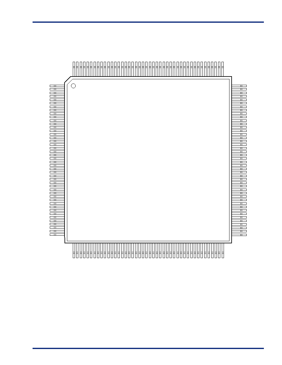
5 4 S X F a m i l y F P G A s
v3.1
43
P a c k a g e P i n A s s i g n m e n t s
(continued)
1 7 6 - P i n T Q F P ( T o p V i e w )
176-Pin
TQFP
176
1
5 4 S X F a m i l y F P G A s
44
v3.1
1 7 6 - P i n T Q F P
Pin Number
A54SX08
Function
A54SX16,
A54SX16P
Function
A54SX32
Function
Pin Number
A54SX08
Function
A54SX16,
A54SX16P
Function
A54SX32
Function
1
GND
GND
GND
45
I/O
I/O
I/O
2
TDI, I/O
TDI, I/O
TDI, I/O
46
I/O
I/O
I/O
3
NC
I/O
I/O
47
I/O
I/O
I/O
4
I/O
I/O
I/O
48
I/O
I/O
I/O
5
I/O
I/O
I/O
49
I/O
I/O
I/O
6
I/O
I/O
I/O
50
I/O
I/O
I/O
7
I/O
I/O
I/O
51
I/O
I/O
I/O
8
I/O
I/O
I/O
52
V
CCI
V
CCI
V
CCI
9
I/O
I/O
I/O
53
I/O
I/O
I/O
10
TMS
TMS
TMS
54
NC
I/O
I/O
11
V
CCI
V
CCI
V
CCI
55
I/O
I/O
I/O
12
NC
I/O
I/O
56
I/O
I/O
I/O
13
I/O
I/O
I/O
57
NC
I/O
I/O
14
I/O
I/O
I/O
58
I/O
I/O
I/O
15
I/O
I/O
I/O
59
I/O
I/O
I/O
16
I/O
I/O
I/O
60
I/O
I/O
I/O
17
I/O
I/O
I/O
61
I/O
I/O
I/O
18
I/O
I/O
I/O
62
I/O
I/O
I/O
19
I/O
I/O
I/O
63
I/O
I/O
I/O
20
I/O
I/O
I/O
64
PRB, I/O
PRB, I/O
PRB, I/O
21
GND
GND
GND
65
GND
GND
GND
22
V
CCA
V
CCA
V
CCA
66
V
CCA
V
CCA
V
CCA
23
GND
GND
GND
67
V
CCR
V
CCR
V
CCR
24
I/O
I/O
I/O
68
I/O
I/O
I/O
25
I/O
I/O
I/O
69
HCLK
HCLK
HCLK
26
I/O
I/O
I/O
70
I/O
I/O
I/O
27
I/O
I/O
I/O
71
I/O
I/O
I/O
28
I/O
I/O
I/O
72
I/O
I/O
I/O
29
I/O
I/O
I/O
73
I/O
I/O
I/O
30
I/O
I/O
I/O
74
I/O
I/O
I/O
31
I/O
I/O
I/O
75
I/O
I/O
I/O
32
V
CCI
V
CCI
V
CCI
76
I/O
I/O
I/O
33
V
CCA
V
CCA
V
CCA
77
I/O
I/O
I/O
34
I/O
I/O
I/O
78
I/O
I/O
I/O
35
I/O
I/O
I/O
79
NC
I/O
I/O
36
I/O
I/O
I/O
80
I/O
I/O
I/O
37
I/O
I/O
I/O
81
NC
I/O
I/O
38
I/O
I/O
I/O
82
V
CCI
V
CCI
V
CCI
39
I/O
I/O
I/O
83
I/O
I/O
I/O
40
NC
I/O
I/O
84
I/O
I/O
I/O
41
I/O
I/O
I/O
85
I/O
I/O
I/O
42
NC
I/O
I/O
86
I/O
I/O
I/O
43
I/O
I/O
I/O
87
TDO, I/O
TDO, I/O
TDO, I/O
44
GND
GND
GND
88
I/O
I/O
I/O

5 4 S X F a m i l y F P G A s
v3.1
45
89
GND
GND
GND
133
GND
GND
GND
90
NC
I/O
I/O
134
I/O
I/O
I/O
91
NC
I/O
I/O
135
I/O
I/O
I/O
92
I/O
I/O
I/O
136
I/O
I/O
I/O
93
I/O
I/O
I/O
137
I/O
I/O
I/O
94
I/O
I/O
I/O
138
I/O
I/O
I/O
95
I/O
I/O
I/O
139
I/O
I/O
I/O
96
I/O
I/O
I/O
140
V
CCI
V
CCI
V
CCI
97
I/O
I/O
I/O
141
I/O
I/O
I/O
98
V
CCA
V
CCA
V
CCA
142
I/O
I/O
I/O
99
V
CCI
V
CCI
V
CCI
143
I/O
I/O
I/O
100
I/O
I/O
I/O
144
I/O
I/O
I/O
101
I/O
I/O
I/O
145
I/O
I/O
I/O
102
I/O
I/O
I/O
146
I/O
I/O
I/O
103
I/O
I/O
I/O
147
I/O
I/O
I/O
104
I/O
I/O
I/O
148
I/O
I/O
I/O
105
I/O
I/O
I/O
149
I/O
I/O
I/O
106
I/O
I/O
I/O
150
I/O
I/O
I/O
107
I/O
I/O
I/O
151
I/O
I/O
I/O
108
GND
GND
GND
152
CLKA
CLKA
CLKA
109
V
CCA
V
CCA
V
CCA
153
CLKB
CLKB
CLKB
110
GND
GND
GND
154
V
CCR
V
CCR
V
CCR
111
I/O
I/O
I/O
155
GND
GND
GND
112
I/O
I/O
I/O
156
V
CCA
V
CCA
V
CCA
113
I/O
I/O
I/O
157
PRA, I/O
PRA, I/O
PRA, I/O
114
I/O
I/O
I/O
158
I/O
I/O
I/O
115
I/O
I/O
I/O
159
I/O
I/O
I/O
116
I/O
I/O
I/O
160
I/O
I/O
I/O
117
I/O
I/O
I/O
161
I/O
I/O
I/O
118
NC
I/O
I/O
162
I/O
I/O
I/O
119
I/O
I/O
I/O
163
I/O
I/O
I/O
120
NC
I/O
I/O
164
I/O
I/O
I/O
121
NC
I/O
I/O
165
I/O
I/O
I/O
122
V
CCA
V
CCA
V
CCA
166
I/O
I/O
I/O
123
GND
GND
GND
167
I/O
I/O
I/O
124
V
CCI
V
CCI
V
CCI
168
NC
I/O
I/O
125
I/O
I/O
I/O
169
V
CCI
V
CCI
V
CCI
126
I/O
I/O
I/O
170
I/O
I/O
I/O
127
I/O
I/O
I/O
171
NC
I/O
I/O
128
I/O
I/O
I/O
172
NC
I/O
I/O
129
I/O
I/O
I/O
173
NC
I/O
I/O
130
I/O
I/O
I/O
174
I/O
I/O
I/O
131
NC
I/O
I/O
175
I/O
I/O
I/O
132
NC
I/O
I/O
176
TCK, I/O
TCK, I/O
TCK, I/O
1 7 6 - P i n T Q F P ( C o n t i n u e d )
Pin Number
A54SX08
Function
A54SX16,
A54SX16P
Function
A54SX32
Function
Pin Number
A54SX08
Function
A54SX16,
A54SX16P
Function
A54SX32
Function
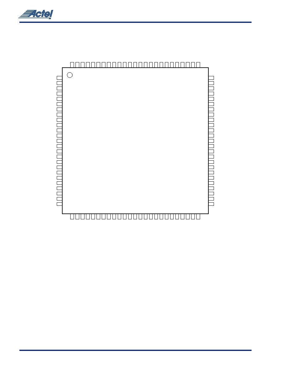
5 4 S X F a m i l y F P G A s
46
v3.1
P a c k a g e P i n A s s i g n m e n t s
(continued)
1 0 0 - P i n V Q F P ( T o p V i e w )
1
100-Pin
VQFP
100

5 4 S X F a m i l y F P G A s
v3.1
47
1 0 0 - V Q F P
Pin Number
A54SX08
Function
A54SX16,
A54SX16P
Function
Pin Number
A54SX08
Function
A54SX16
A54SX16P
Function
1
GND
GND
51
GND
GND
2
TDI, I/O
TDI, I/O
52
I/O
I/O
3
I/O
I/O
53
I/O
I/O
4
I/O
I/O
54
I/O
I/O
5
I/O
I/O
55
I/O
I/O
6
I/O
I/O
56
I/O
I/O
7
TMS
TMS
57
V
CCA
V
CCA
8
V
CCI
V
CCI
58
V
CCI
V
CCI
9
GND
GND
59
I/O
I/O
10
I/O
I/O
60
I/O
I/O
11
I/O
I/O
61
I/O
I/O
12
I/O
I/O
62
I/O
I/O
13
I/O
I/O
63
I/O
I/O
14
I/O
I/O
64
I/O
I/O
15
I/O
I/O
65
I/O
I/O
16
I/O
I/O
66
I/O
I/O
17
I/O
I/O
67
V
CCA
V
CCA
18
I/O
I/O
68
GND
GND
19
I/O
I/O
69
GND
GND
20
V
CCI
V
CCI
70
I/O
I/O
21
I/O
I/O
71
I/O
I/O
22
I/O
I/O
72
I/O
I/O
23
I/O
I/O
73
I/O
I/O
24
I/O
I/O
74
I/O
I/O
25
I/O
I/O
75
I/O
I/O
26
I/O
I/O
76
I/O
I/O
27
I/O
I/O
77
I/O
I/O
28
I/O
I/O
78
I/O
I/O
29
I/O
I/O
79
I/O
I/O
30
I/O
I/O
80
I/O
I/O
31
I/O
I/O
81
I/O
I/O
32
I/O
I/O
82
V
CCI
V
CCI
33
I/O
I/O
83
I/O
I/O
34
PRB, I/O
PRB, I/O
84
I/O
I/O
35
V
CCA
V
CCA
85
I/O
I/O
36
GND
GND
86
I/O
I/O
37
V
CCR
V
CCR
87
CLKA
CLKA
38
I/O
I/O
88
CLKB
CLKB
39
HCLK
HCLK
89
V
CCR
V
CCR
40
I/O
I/O
90
V
CCA
V
CCA
41
I/O
I/O
91
GND
GND
42
I/O
I/O
92
PRA, I/O
PRA, I/O
43
I/O
I/O
93
I/O
I/O
44
V
CCI
V
CCI
94
I/O
I/O
45
I/O
I/O
95
I/O
I/O
46
I/O
I/O
96
I/O
I/O
47
I/O
I/O
97
I/O
I/O
48
I/O
I/O
98
I/O
I/O
49
TDO, I/O
TDO, I/O
99
I/O
I/O
50
I/O
I/O
100
TCK, I/O
TCK, I/O

5 4 S X F a m i l y F P G A s
48
v3.1
P a c k a g e P i n A s s i g n m e n t s
(continued)
313-Pin PBGA (Top View)
1
2
3
4
5
6
7
8
9 10 11 12 13 14 15
A
B
C
D
E
F
G
H
J
K
L
M
N
P
R
T
U
V
W
Y
AA
AB
AC
AD
AE
A
B
C
D
E
F
G
H
J
K
L
M
N
P
R
T
U
V
W
Y
AA
AB
AC
AD
AE
16 17 18 19 20 21 22 23 24 25
1
2
3
4
5
6
7
8
9 10 11 12 13 14 15 16 17 18 19 20 21 22 23 24 25
5 4 S X F a m i l y F P G A s
v3.1
49
3 1 3 - P i n P B G A
Pin Number
A54SX32
Function
Pin Number
A54SX32
Function
Pin Number
A54SX32
Function
Pin Number
A54SX32
Function
A1
GND
AC15
I/O
C5
NC
F20
I/O
A3
NC
AC17
I/O
C7
I/O
F22
I/O
A5
I/O
AC19
I/O
C9
I/O
F24
I/O
A7
I/O
AC21
I/O
C11
I/O
G1
I/O
A9
I/O
AC23
I/O
C13
V
CCI
G3
TMS
A11
I/O
AC25
NC
C15
I/O
G5
I/O
A13
V
CCR
AD2
GND
C17
I/O
G7
I/O
A15
I/O
AD4
I/O
C19
V
CCI
G9
V
CCI
A17
I/O
AD6
V
CCI
C21
I/O
G11
I/O
A19
I/O
AD8
I/O
C23
I/O
G13
CLKB
A21
I/O
AD10
I/O
C25
NC
G15
I/O
A23
NC
AD12
PRB, I/O
D2
I/O
G17
I/O
A25
GND
AD14
I/O
D4
NC
G19
I/O
AA1
I/O
AD16
I/O
D6
I/O
G21
I/O
AA3
I/O
AD18
I/O
D8
I/O
G23
I/O
AA5
NC
AD20
I/O
D10
I/O
G25
I/O
AA7
I/O
AD22
NC
D12
I/O
H2
I/O
AA9
NC
AD24
I/O
D14
I/O
H4
I/O
AA11
I/O
AE1
NC
D16
I/O
H6
I/O
AA13
I/O
AE3
I/O
D18
I/O
H8
I/O
AA15
I/O
AE5
I/O
D20
I/O
H10
I/O
AA17
I/O
AE7
I/O
D22
I/O
H12
PRA, I/O
AA19
I/O
AE9
I/O
D24
NC
H14
I/O
AA21
I/O
AE11
I/O
E1
I/O
H16
I/O
AA23
NC
AE13
V
CCA
E3
NC
H18
NC
AA25
I/O
AE15
I/O
E5
I/O
H20
I/O
AB2
NC
AE17
I/O
E7
I/O
H22
V
CCI
AB4
NC
AE19
I/O
E9
I/O
H24
I/O
AB6
I/O
AE21
I/O
E11
I/O
J1
I/O
AB8
I/O
AE23
TDO, I/O
E13
V
CCA
J3
I/O
AB10
I/O
AE25
GND
E15
I/O
J5
I/O
AB12
I/O
B2
TCK, I/O
E17
I/O
J7
NC
AB14
I/O
B4
I/O
E19
I/O
J9
I/O
AB16
I/O
B6
I/O
E21
I/O
J11
I/O
AB18
V
CCI
B8
I/O
E23
I/O
J13
CLKA
AB20
NC
B10
I/O
E25
I/O
J15
I/O
AB22
I/O
B12
I/O
F2
I/O
J17
I/O
AB24
I/O
B14
I/O
F4
I/O
J19
I/O
AC1
I/O
B16
I/O
F6
NC
J21
GND
AC3
I/O
B18
I/O
F8
I/O
J23
I/O
AC5
I/O
B20
I/O
F10
NC
J25
I/O
AC7
I/O
B22
I/O
F12
I/O
K2
I/O
AC9
I/O
B24
I/O
F14
I/O
K4
I/O
AC11
I/O
C1
TDI, I/O
F16
NC
K6
I/O
AC13
V
CCR
C3
I/O
F18
I/O
K8
V
CCI
5 4 S X F a m i l y F P G A s
50
v3.1
K10
I/O
N3
V
CCA
R21
I/O
V18
I/O
K12
I/O
N5
V
CCR
R23
I/O
V20
I/O
K14
I/O
N7
I/O
R25
I/O
V22
V
CCA
K16
I/O
N9
V
CCI
T2
I/O
V24
V
CCI
K18
I/O
N11
GND
T4
I/O
W1
I/O
K20
V
CCA
N13
GND
T6
I/O
W3
I/O
K22
I/O
N15
GND
T8
I/O
W5
I/O
K24
I/O
N17
I/O
T10
I/O
W7
NC
L1
I/O
N19
I/O
T12
I/O
W9
I/O
L3
I/O
N21
I/O
T14
HCLK
W11
I/O
L5
I/O
N23
V
CCR
T16
I/O
W13
V
CCI
L7
I/O
N25
V
CCA
T18
I/O
W15
I/O
L9
I/O
P2
I/O
T20
I/O
W17
I/O
L11
I/O
P4
I/O
T22
I/O
W19
I/O
L13
GND
P6
I/O
T24
I/O
W21
I/O
L15
I/O
P8
I/O
U1
I/O
W23
I/O
L17
I/O
P10
I/O
U3
I/O
W25
I/O
L19
I/O
P12
GND
U5
V
CCI
Y2
I/O
L21
I/O
P14
GND
U7
I/O
Y4
I/O
L23
I/O
P16
I/O
U9
I/O
Y6
I/O
L25
I/O
P18
I/O
U15
I/O
Y8
I/O
M2
I/O
P20
NC
U17
I/O
Y10
I/O
M4
I/O
P22
I/O
U19
I/O
Y12
I/O
M6
I/O
P24
I/O
U21
I/O
Y14
I/O
M8
I/O
R1
I/O
U23
I/O
Y16
I/O
M10
I/O
R3
I/O
U25
I/O
Y18
I/O
M12
GND
R5
I/O
V2
V
CCA
Y20
NC
M14
GND
R7
I/O
V4
I/O
Y22
I/O
M16
V
CCI
R9
I/O
V6
I/O
Y24
NC
M18
I/O
R11
I/O
V8
I/O
M20
I/O
R13
GND
V10
I/O
M22
I/O
R15
I/O
V12
I/O
M24
I/O
R17
I/O
V14
I/O
N1
I/O
R19
I/O
V16
NC
3 1 3 - P i n P B G A ( C o n t i n u e d )
Pin Number
A54SX32
Function
Pin Number
A54SX32
Function
Pin Number
A54SX32
Function
Pin Number
A54SX32
Function
5 4 S X F a m i l y F P G A s
v3.1
51
P a c k a g e P i n A s s i g n m e n t s
(continued)
329-Pin PBGA (Top View)
23
22
21
20
19
18
17
16
15
14
10 11 12 13
9
8
7
6
5
4
3
2
1
A
B
C
D
E
F
G
H
J
K
L
M
N
P
R
T
U
V
W
Y
AA
AB
AC
5 4 S X F a m i l y F P G A s
52
v3.1
3 2 9 - P i n P B G A
Pin Number
A54SX32
Function
Pin Number
A54SX32
Function
Pin Number
A54SX32
Function
Pin Number
A54SX32
Function
A1
GND
AA23
V
CCI
AC22
V
CCI
C21
V
CCI
A2
GND
AB1
I/O
AC23
GND
C22
GND
A3
V
CCI
AB2
GND
B1
V
CCI
C23
NC
A4
NC
AB3
I/O
B2
GND
D1
I/O
A5
I/O
AB4
I/O
B3
I/O
D2
I/O
A6
I/O
AB5
I/O
B4
I/O
D3
I/O
A7
V
CCI
AB6
I/O
B5
I/O
D4
TCK, I/O
A8
NC
AB7
I/O
B6
I/O
D5
I/O
A9
I/O
AB8
I/O
B7
I/O
D6
I/O
A10
I/O
AB9
I/O
B8
I/O
D7
I/O
A11
I/O
AB10
I/O
B9
I/O
D8
I/O
A12
I/O
AB11
PRB, I/O
B10
I/O
D9
I/O
A13
CLKB
AB12
I/O
B11
I/O
D10
I/O
A14
I/O
AB13
HCLK
B12
PRA, I/O
D11
V
CCA
A15
I/O
AB14
I/O
B13
CLKA
D12
V
CCR
A16
I/O
AB15
I/O
B14
I/O
D13
I/O
A17
I/O
AB16
I/O
B15
I/O
D14
I/O
A18
I/O
AB17
I/O
B16
I/O
D15
I/O
A19
I/O
AB18
I/O
B17
I/O
D16
I/O
A20
I/O
AB19
I/O
B18
I/O
D17
I/O
A21
NC
AB20
I/O
B19
I/O
D18
I/O
A22
V
CCI
AB21
I/O
B20
I/O
D19
I/O
A23
GND
AB22
GND
B21
I/O
D20
I/O
AA1
V
CCI
AB23
I/O
B22
GND
D21
I/O
AA2
I/O
AC1
GND
B23
V
CCI
D22
I/O
AA3
GND
AC2
V
CCI
C1
NC
D23
I/O
AA4
I/O
AC3
NC
C2
TDI, I/O
E1
V
CCI
AA5
I/O
AC4
I/O
C3
GND
E2
I/O
AA6
I/O
AC5
I/O
C4
I/O
E3
I/O
AA7
I/O
AC6
I/O
C5
I/O
E4
I/O
AA8
I/O
AC7
I/O
C6
I/O
E20
I/O
AA9
I/O
AC8
I/O
C7
I/O
E21
I/O
AA10
I/O
AC9
V
CCI
C8
I/O
E22
I/O
AA11
I/O
AC10
I/O
C9
I/O
E23
I/O
AA12
I/O
AC11
I/O
C10
I/O
F1
I/O
AA13
I/O
AC12
I/O
C11
I/O
F2
TMS
AA14
I/O
AC13
I/O
C12
I/O
F3
I/O
AA15
I/O
AC14
I/O
C13
I/O
F4
I/O
AA16
I/O
AC15
NC
C14
I/O
F20
I/O
AA17
I/O
AC16
I/O
C15
I/O
F21
I/O
AA18
I/O
AC17
I/O
C16
I/O
F22
I/O
AA19
I/O
AC18
I/O
C17
I/O
F23
I/O
AA20
TDO, I/O
AC19
I/O
C18
I/O
G1
I/O
AA21
V
CCI
AC20
I/O
C19
I/O
G2
I/O
AA22
I/O
AC21
NC
C20
I/O
G3
I/O

5 4 S X F a m i l y F P G A s
v3.1
53
G4
I/O
L22
I/O
R20
I/O
Y10
I/O
G20
I/O
L23
NC
R21
I/O
Y11
I/O
G21
I/O
M1
I/O
R22
I/O
Y12
V
CCA
G22
I/O
M2
I/O
R23
I/O
Y13
V
CCR
G23
GND
M3
I/O
T1
I/O
Y14
I/O
H1
I/O
M4
V
CCA
T2
I/O
Y15
I/O
H2
I/O
M10
GND
T3
I/O
Y16
I/O
H3
I/O
M11
GND
T4
I/O
Y17
I/O
H4
I/O
M12
GND
T20
I/O
Y18
I/O
H20
V
CCA
M13
GND
T21
I/O
Y19
I/O
H21
I/O
M14
GND
T22
I/O
Y20
GND
H22
I/O
M20
V
CCA
T23
I/O
Y21
I/O
H23
I/O
M21
I/O
U1
I/O
Y22
I/O
J1
NC
M22
I/O
U2
I/O
Y23
I/O
J2
I/O
M23
V
CCI
U3
V
CCA
J3
I/O
N1
I/O
U4
I/O
J4
I/O
N2
I/O
U20
I/O
J20
I/O
N3
I/O
U21
V
CCA
J21
I/O
N4
I/O
U22
I/O
J22
I/O
N10
GND
U23
I/O
J23
I/O
N11
GND
V1
V
CCI
K1
I/O
N12
GND
V2
I/O
K2
I/O
N13
GND
V3
I/O
K3
I/O
N14
GND
V4
I/O
K4
I/O
N20
NC
V20
I/O
K10
GND
N21
I/O
V21
I/O
K11
GND
N22
I/O
V22
I/O
K12
GND
N23
I/O
V23
I/O
K13
GND
P1
I/O
W1
I/O
K14
GND
P2
I/O
W2
I/O
K20
I/O
P3
I/O
W3
I/O
K21
I/O
P4
I/O
W4
I/O
K22
I/O
P10
GND
W20
I/O
K23
I/O
P11
GND
W21
I/O
L1
I/O
P12
GND
W22
I/O
L2
I/O
P13
GND
W23
NC
L3
I/O
P14
GND
Y1
NC
L4
V
CCR
P20
I/O
Y2
I/O
L10
GND
P21
I/O
Y3
I/O
L11
GND
P22
I/O
Y4
GND
L12
GND
P23
I/O
Y5
I/O
L13
GND
R1
I/O
Y6
I/O
L14
GND
R2
I/O
Y7
I/O
L20
V
CCR
R3
I/O
Y8
I/O
L21
I/O
R4
I/O
Y9
I/O
3 2 9 - P i n P B G A
Pin Number
A54SX32
Function
Pin Number
A54SX32
Function
Pin Number
A54SX32
Function
Pin Number
A54SX32
Function
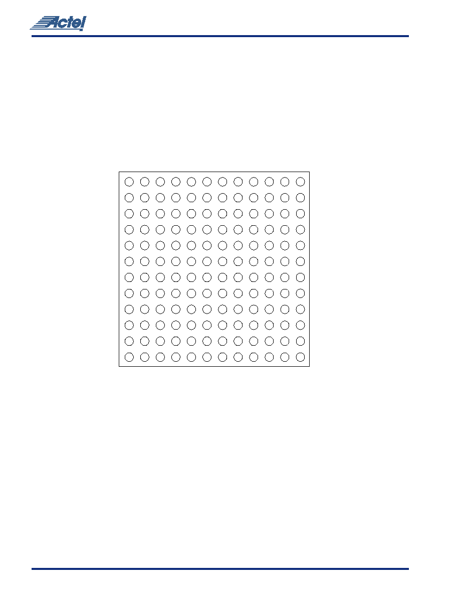
5 4 S X F a m i l y F P G A s
54
v3.1
P a c k a g e P i n A s s i g n m e n t s
(Continued)
144-Pin FBGA (Top View)
1
2
3
4
5
6
7
8
9
10
11
12
A
B
C
D
E
F
G
H
J
K
L
M

5 4 S X F a m i l y F P G A s
v3.1
55
1 4 4 - P i n F B G A
Pin Number
A54SX08
Function
Pin Number
A54SX08
Function
Pin Number
A54SX08
Function
A1
I/O
E1
I/O
J1
I/O
A2
I/O
E2
I/O
J2
I/O
A3
I/O
E3
I/O
J3
I/O
A4
I/O
E4
I/O
J4
I/O
A5
V
CCA
E5
TMS
J5
I/O
A6
GND
E6
V
CCI
J6
PRB, I/O
A7
CLKA
E7
V
CCI
J7
I/O
A8
I/O
E8
V
CCI
J8
I/O
A9
I/O
E9
V
CCA
J9
I/O
A10
I/O
E10
I/O
J10
I/O
A11
I/O
E11
GND
J11
I/O
A12
I/O
E12
I/O
J12
V
CCA
B1
I/O
F1
I/O
K1
I/O
B2
GND
F2
I/O
K2
I/O
B3
I/O
F3
V
CCR
K3
I/O
B4
I/O
F4
I/O
K4
I/O
B5
I/O
F5
GND
K5
I/O
B6
I/O
F6
GND
K6
I/O
B7
CLKB
F7
GND
K7
GND
B8
I/O
F8
V
CCI
K8
I/O
B9
I/O
F9
I/O
K9
I/O
B10
I/O
F10
GND
K10
GND
B11
GND
F11
I/O
K11
I/O
B12
I/O
F12
I/O
K12
I/O
C1
I/O
G1
I/O
L1
GND
C2
I/O
G2
GND
L2
I/O
C3
TCK, I/O
G3
I/O
L3
I/O
C4
I/O
G4
I/O
L4
I/O
C5
I/O
G5
GND
L5
I/O
C6
PRA, I/O
G6
GND
L6
I/O
C7
I/O
G7
GND
L7
HCLK
C8
I/O
G8
V
CCI
L8
I/O
C9
I/O
G9
I/O
L9
I/O
C10
I/O
G10
I/O
L10
I/O
C11
I/O
G11
I/O
L11
I/O
C12
I/O
G12
I/O
L12
I/O
D1
I/O
H1
I/O
M1
I/O
D2
V
CCI
H2
I/O
M2
I/O
D3
TDI, I/O
H3
I/O
M3
I/O
D4
I/O
H4
I/O
M4
I/O
D5
I/O
H5
V
CCA
M5
I/O
D6
I/O
H6
V
CCA
M6
I/O
D7
I/O
H7
V
CCI
M7
V
CCA
D8
I/O
H8
V
CCI
M8
I/O
D9
I/O
H9
V
CCA
M9
I/O
D10
I/O
H10
I/O
M10
I/O
D11
I/O
H11
I/O
M11
TDO, I/O
D12
I/O
H12
V
CCR
M12
I/O

5 4 S X F a m i l y F P G A s
56 v3.1
L i s t o f C h a n g e s
The following table lists critical changes that were made in the current version of the document.
D a t a s h e e t C a t e g o r i e s
In order to provide the latest information to designers, some datasheets are published before data has been fully
characterized. Datasheets are designated as "Product Brief," "Advanced," "Production." The definition of these categories
are as follows:
P r o d u c t B r i e f
The product brief is a modified version of an advanced datasheet containing general product information. This brief
summarizes specific device and family information for unreleased products.
A d v a n c e d
This datasheet version contains initial estimated information based on simulation, other products, devices, or speed grades.
This information can be used as estimates but not for production.
U n m a r k e d ( p r o d u c t i o n )
This datasheet version contains information that is considered to be final.
Previous version
Changes in current version (v3.1)
Page
v3.0.1
The storage temperature in the
"Absolute Maximum Ratings
1
" table on page 10
was
updated.
page 10
Table 1 on page 8
was updated.
page 8

Actel and the Actel logo are registered trademarks of Actel Corporation.
All other trademarks are the property of their owners.
http://www.actel.com
Actel Corporation
955 East Arques Avenue
Sunnyvale, California 94086
USA
Tel: (408) 739-1010
Fax:
(408) 739-1540
Actel Europe Ltd.
Dunlop House, Riverside Way
Camberley, Surrey GU15 3YL
United Kingdom
Tel: +44 (0)1276 401450
Fax: +44 (0)1276 401490
Actel Japan
EXOS Ebisu Bldg. 4F
1-24-14 Ebisu Shibuya-ku
Tokyo 150 Japan
Tel: +81 03-3445-7671
Fax: +81 03-3445-7668
Actel Hong Kong
39th Floor
One Pacific Place
88 Queensway
Admiralty, Hong Kong
Tel: 852-22735712
572137-4/6.03