REV. B
Information furnished by Analog Devices is believed to be accurate and
reliable. However, no responsibility is assumed by Analog Devices for its
use, nor for any infringements of patents or other rights of third parties
which may result from its use. No license is granted by implication or
otherwise under any patent or patent rights of Analog Devices.
a
AD536A
One Technology Way, P.O. Box 9106, Norwood, MA 02062-9106, U.S.A.
Tel: 781/329-4700
World Wide Web Site: http://www.analog.com
Fax: 781/326-8703
© Analog Devices, Inc., 1999
Integrated Circuit
True RMS-to-DC Converter
FEATURES
True RMS-to-DC Conversion
Laser-Trimmed to High Accuracy
0.2% Max Error (AD536AK)
0.5% Max Error (AD536AJ)
Wide Response Capability:
Computes RMS of AC and DC Signals
450 kHz Bandwidth: V rms > 100 mV
2 MHz Bandwidth: V rms > 1 V
Signal Crest Factor of 7 for 1% Error
dB Output with 60 dB Range
Low Power: 1.2 mA Quiescent Current
Single or Dual Supply Operation
Monolithic Integrated Circuit
≠55 C to +125 C Operation (AD536AS)
PRODUCT DESCRIPTION
The AD536A is a complete monolithic integrated circuit which
performs true rms-to-dc conversion. It offers performance which
is comparable or superior to that of hybrid or modular units
costing much more. The AD536A directly computes the true
rms value of any complex input waveform containing ac and dc
components. It has a crest factor compensation scheme which
allows measurements with 1% error at crest factors up to 7. The
wide bandwidth of the device extends the measurement capabi-
lity to 300 kHz with 3 dB error for signal levels above 100 mV.
An important feature of the AD536A not previously available in
rms converters is an auxiliary dB output. The logarithm of the
rms output signal is brought out to a separate pin to allow the
dB conversion, with a useful dynamic range of 60 dB. Using an
externally supplied reference current, the 0 dB level can be con-
veniently set by the user to correspond to any input level from
0.1 to 2 volts rms.
The AD536A is laser trimmed at the wafer level for input and
output offset, positive and negative waveform symmetry (dc re-
versal error), and full-scale accuracy at 7 V rms. As a result, no
external trims are required to achieve the rated unit accuracy.
There is full protection for both inputs and outputs. The input
circuitry can take overload voltages well beyond the supply lev-
els. Loss of supply voltage with inputs connected will not cause
unit failure. The output is short-circuit protected.
The AD536A is available in two accuracy grades (J, K) for com-
mercial temperature range (0
∞C to +70∞C) applications, and one
grade (S) rated for the ≠55
∞C to +125∞C extended range. The
AD536AK offers a maximum total error of
±2 mV ±0.2% of
reading, and the AD536AJ and AD536AS have maximum errors
of
±5 mV ±0.5% of reading. All three versions are available in
either a hermetically sealed 14-lead DIP or 10-pin TO-100
metal can. The AD536AS is also available in a 20-leadless her-
metically sealed ceramic chip carrier.
PRODUCT HIGHLIGHTS
1. The AD536A computes the true root-mean-square level of a
complex ac (or ac plus dc) input signal and gives an equiva-
lent dc output level. The true rms value of a waveform is a
more useful quantity than the average rectified value since it
relates directly to the power of the signal. The rms value of a
statistical signal also relates to its standard deviation.
2. The crest factor of a waveform is the ratio of the peak signal
swing to the rms value. The crest factor compensation
scheme of the AD536A allows measurement of highly com-
plex signals with wide dynamic range.
3. The only external component required to perform measure-
ments to the fully specified accuracy is the capacitor which
sets the averaging period. The value of this capacitor determines
the low frequency ac accuracy, ripple level and settling time.
4. The AD536A will operate equally well from split supplies or
a single supply with total supply levels from 5 to 36 volts.
The one milliampere quiescent supply current makes the
device well-suited for a wide variety of remote controllers and
battery powered instruments.
5. The AD536A directly replaces the AD536 and provides im-
proved bandwidth and temperature drift specifications.
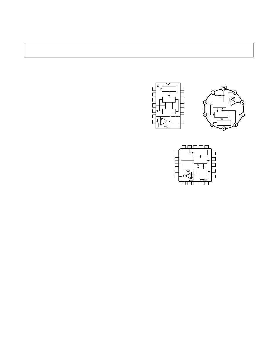
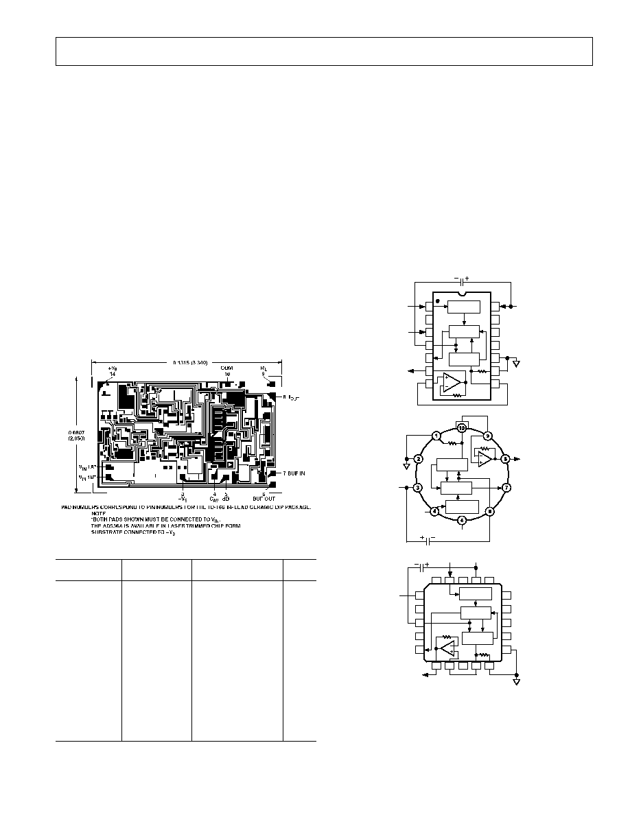
PIN CONFIGURATIONS AND
FUNCTIONAL BLOCK DIAGRAMS
LCC (E-20A) Package
4
5
6
7
8
3 2 1 20 19
18
17
16
15
14
9 10
11 12 13
BUF
CURRENT
MIRROR
ABSOLUTE
VALUE
SQUARER
DIVIDER
25k
25k
AD536A
V
IN
NC
C
AV
dB
+V
S
NC
NC
NC
COM
R
L
I
OUT
NC = NO CONNECT
≠V
S
BUF
OUT
BUF
IN
NC
NC
NC
NC
NC
NC
TO-116 (D-14) and
Q-14 Package
14
13
12
11
10
9
8
1
2
3
4
5
6
7
ABSOLUTE
VALUE
CURRENT
MIRROR
25k
25k
BUF
SQUARER
DIVIDER
AD536A
NC = NO CONNECT
V
IN
NC
≠V
S
C
AV
dB
BUF
OUT
BUF
IN
+V
S
NC
NC
NC
COM
R
L
I
OUT
TO-100 (H-10A)
Package
BUF
25k
ABSOLUTE
VALUE
SQUARER
DIVIDER
CURRENT
MIRROR
25k
AD536A
V
IN
C
AV
dB
+V
S
COM
R
L
I
OUT
≠V
S
BUF
OUT
BUF IN

REV. B
≠2≠
AD536A≠SPECIFICATIONS
Model
AD536AJ
AD536AK
AD536AS
Min
Typ
Max
Min
Typ
Max
Min
Typ
Max
Units
TRANSFER FUNCTION
V
OUT
= avg .(V
IN
)
2
V
OUT
= avg .(V
IN
)
2
V
OUT
= avg .(V
IN
)
2
CONVERSION ACCURACY
Total Error, Internal Trim
1
(Figure 1)
5 0.5
2 0.2
5 0.5
mV
± % of Reading
vs. Temperature, T
MIN
to +70
∞C
±0.1 ±0.01
±0.05 ±0.005
0.1 0.005
mV
± % of Reading/∞C
+70
∞C to +125∞C
0.3 0.005
mV
± % of Reading/∞C
vs. Supply Voltage
±0.1 ±0.01
±0.1 ±0.01
±0.1 ±0.01
mV
± % of Reading/V
dc Reversal Error
±0.2
±0.1
±0.2
± % of Reading
Total Error, External Trim
1
(Figure 2)
±3 ±0.3
±2 ±0.1
±3 ±0.3
mV
± % of Reading
ERROR VS. CREST FACTOR
2
Crest Factor 1 to 2
Specified Accuracy Specified Accuracy
Specified Accuracy
Crest Factor = 3
≠0.1
≠0.1
≠0.1
% of Reading
Crest Factor = 7
≠1.0
≠1.0
≠1.0
% of Reading
FREQUENCY RESPONSE
3
Bandwidth for 1% Additional Error (0.09 dB)
V
IN
= 10 mV
5
5
5
kHz
V
IN
= 100 mV
45
45
45
kHz
V
IN
= 1 V
120
120
120
kHz
±3 dB Bandwidth
V
IN
= 10 mV
90
90
90
kHz
V
IN
= 100 mV
450
450
450
kHz
V
IN
= 1 V
2.3
2.3
2.3
MHz
AVERAGlNG TlME CONSTANT (Figure 5)
25
25
25
ms/
µF CAV
INPUT CHARACTERISTICS
Signal Range,
±15 V Supplies
Continuous rms Level
0 to 7
0 to 7
0 to 7
V rms
Peak Transient Input
±20
±20
±20
V peak
Continuous rms Level,
±5 V Supplies
0 to 2
0 to 2
0 to 2
V rms
Peak Transient Input,
±5 V Supplies
±7
±7
±7
V peak
Maximum Continuous Nondestructive
Input Level (All Supply Voltages)
±25
±25
±25
V peak
Input Resistance
13.33
16.67
20
13.33
16.67
20
13.33
16.67
20
k
Input Offset Voltage
0.8
±2
0.5
±1
0.8
±2
mV
OUTPUT CHARACTERISTICS
Offset Voltage, V
IN
= COM (Figure 1)
±1
±2
±0.5
±1
2
mV
vs. Temperature
±0.1
±0.1
0.2
mV/
∞C
vs. Supply Voltage
±0.1
±0.1
±0.2
mV/V
Voltage Swing,
±15 V Supplies
0 to +11
+12.5
0 to +11
+12.5
0 to +11
+12.5
V
±5 V Supply
0 to +2
0 to +2
0 to +2
V
dB OUTPUT (Figure 13)
Error, V
lN
7 mV to 7 V rms, 0 dB = 1 V rms
±0.4
0.6
±0.2
0.3
±0.5
0.6
dB
Scale Factor
≠3
≠3
≠3
mV/dB
Scale Factor TC (Uncompensated, see Fig-
ure 1 for Temperature Compensation)
≠0.033
≠0.033
≠0.033
dB/
∞C
+0.33
+0.33
+0.33
% of Reading/
∞C
I
REF
for 0 dB = 1 V rms
5
20
80
5
20
80
5
20
80
µA
I
REF
Range
1
100
1
100
1
100
µA
I
OUT
TERMINAL
I
OUT
Scale Factor
40
40
40
µA/V rms
I
OUT
Scale Factor Tolerance
±10
±20
±10
±20
±10
±20
%
Output Resistance
20
25
30
20
25
30
20
25
30
k
Voltage Compliance
≠V
S
to (+V
S
≠V
S
to (+V
S
≠V
S
to (+V
S
≠2.5 V)
≠2.5 V)
≠2.5 V)
V
BUFFER AMPLIFIER
Input and Output Voltage Range
≠V
S
to (+V
S
≠V
S
to (+V
S
≠V
S
to (+V
S
V
≠2.5 V)
≠2.5 V)
≠2.5 V)
Input Offset Voltage, R
S
= 25 k
±0.5
4
±0.5
4
±0.5
4
mV
Input Bias Current
20
60
20
60
20
60
nA
Input Resistance
10
8
10
8
10
8
Output Current
(+5 mA,
(+5 mA,
(+5 mA,
≠130
µA)
≠130
µA)
≠130
µA)
Short Circuit Current
20
20
20
mA
Output Resistance
0.5
0.5
0.5
Small Signal Bandwidth
1
1
1
MHz
Slew Rate
4
5
5
5
V/
µs
POWER SUPPLY
Voltage Rated Performance
±15
±15
±15
V
Dual Supply
±3.0
±18
±3.0
±18
±3.0
±18
V
Single Supply
+5
+36
+5
+36
+5
+36
V
Quiescent Current
Total V
S
, 5 V to 36 V, T
MIN
to T
MAX
1.2
2
1.2
2
1.2
2
mA
TEMPERATURE RANGE
Rated Performance
0
+70
0
+70
≠55
+125
∞C
Storage
≠55
+150
≠55
+150
≠55
+150
∞C
NUMBER OF TRANSISTORS
65
65
65
NOTES
1
Accuracy is specified for 0 V to 7 V rms, dc or 1 kHz sine wave input with the AD536A connected as in the figure referenced.
2
Error vs. crest factor is specified as an additional error for 1 V rms rectangular pulse input, pulsewidth = 200
µs.
3
Input voltages are expressed in volts rms, and error is percent of reading.
4
With 2k external pull-down resistor.
Specifications subject to change without notice.
Specifications shown in boldface are tested on all production units at final electrical test. Results from those tests are used to calculate outgoing quality levels. All min and max specifications are guaranteed,
although only those shown in boldface are tested on all production units.
(@ +25 C, and 15 V dc unless otherwise noted)
REV. B
AD536A
≠3≠
ABSOLUTE MAXIMUM RATINGS
1
Supply Voltage
Dual Supply . . . . . . . . . . . . . . . . . . . . . . . . . . . . . . . .
±18 V
Single Supply . . . . . . . . . . . . . . . . . . . . . . . . . . . . . . . +36 V
Internal Power Dissipation
2
. . . . . . . . . . . . . . . . . . . . 500 mW
Maximum Input Voltage . . . . . . . . . . . . . . . . . . . .
±25 V Peak
Buffer Maximum Input Voltage . . . . . . . . . . . . . . . . . . . . .
±V
S
Maximum Input Voltage . . . . . . . . . . . . . . . . . . . .
±25 V Peak
Storage Temperature Range . . . . . . . . . . . . ≠55
∞C to +150∞C
Operating Temperature Range
AD536AJ/K . . . . . . . . . . . . . . . . . . . . . . . . . . 0
∞C to +70∞C
AD536AS . . . . . . . . . . . . . . . . . . . . . . . . ≠55
∞C to +125∞C
Lead Temperature Range
(Soldering 60 sec) . . . . . . . . . . . . . . . . . . . . . . . . . . +300
∞C
ESD Rating . . . . . . . . . . . . . . . . . . . . . . . . . . . . . . . . . 1000 V
NOTES
1
Stresses above those listed under Absolute Maximum Ratings may cause perma-
nent damage to the device. This is a stress rating only; functional operation of the
device at these or any other conditions above those indicated in the operational
section of this specification is not implied. Exposure to absolute maximum rating
conditions for extended periods may affect device reliability.
2
10-Pin Header:
JA
= 150
∞C/W; 20-Leadless LCC:
JA
= 95
∞C/W; 14-Lead Size
Brazed Ceramic DIP:
JA
= 95
∞C/W.
CHIP DIMENSIONS AND PAD LAYOUT
Dimensions shown in inches and (mm).
ORDERING GUIDE
Temperature
Package
Package
Model
Range
Description
Option
AD536AJD
0
∞C to +70∞C
Side Brazed Ceramic DIP
D-14
AD536AKD
0
∞C to +70∞C
Side Brazed Ceramic DIP
D-14
AD536AJH
0
∞C to +70∞C
Header
H-10A
AD536AKH
0
∞C to +70∞C
Header
H-10A
AD536AJQ
0
∞C to +70∞C
Cerdip
Q-14
AD536AKQ
0
∞C to +70∞C
Cerdip
Q-14
AD536ASD
≠55
∞C to +125∞C
Side Brazed Ceramic DIP
D-14
AD536ASD/883B
≠55
∞C to +125∞C
Side Brazed Ceramic DIP
D-14
AD536ASE/883B
≠55
∞C to +125∞C
LCC
E-20A
AD536ASH
≠55
∞C to +125∞C
Header
H-10A
AD536ASH/883B
≠55
∞C to +125∞C
Header
H-10A
AD536AJCHIPS
0
∞C to +70∞C
Die
AD536AKH/+
0
∞C to +70∞C
Header
H-10A
AD536ASCHIPS
≠55
∞C to +125∞C
Die
5962-89805012A
≠55
∞C to +125∞C
LCC
E-20A
5962-8980501CA
≠55
∞C to +125∞C
Side Brazed Ceramic DIP
D-14
5962-8980501IA
≠55
∞C to +125∞C
Header
H-10A
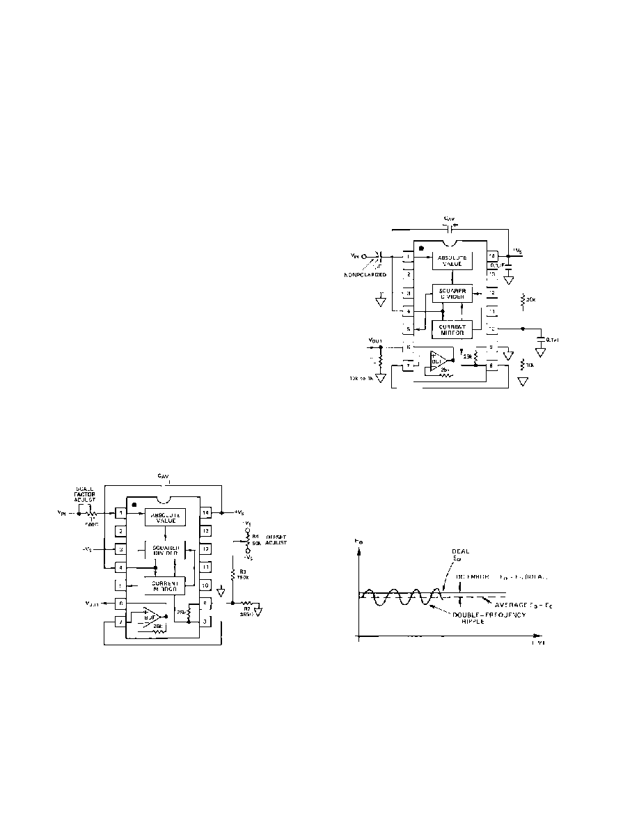
STANDARD CONNECTION
The AD536A is simple to connect for the majority of high accu-
racy rms measurements, requiring only an external capacitor to
set the averaging time constant. The standard connection is
shown in Figure 1. In this configuration, the AD536A will mea-
sure the rms of the ac and dc level present at the input, but will
show an error for low frequency inputs as a function of the filter
capacitor, C
AV
, as shown in Figure 5. Thus, if a 4
µF capacitor
is used, the additional average error at 10 Hz will be 0.1%, at
3 Hz it will be 1%. The accuracy at higher frequencies will be
according to specification. If it is desired to reject the dc input, a
capacitor is added in series with the input, as shown in Figure 3,
the capacitor must be nonpolar. If the AD536A is driven with
power supplies with a considerable amount of high frequency
ripple, it is advisable to bypass both supplies to ground with
0.1
µF ceramic discs as near the device as possible.
V
IN
+V
S
≠V
S
V
OUT
C
AV
BUF
25k
ABSOLUTE
VALUE
SQUARER
DIVIDER
CURRENT
MIRROR
25k
AD536A
14
13
12
11
10
9
8
1
2
3
4
5
6
7
ABSOLUTE
VALUE
CURRENT
MIRROR
25k
25k
BUF
SQUARER
DIVIDER
AD536A
V
IN
≠V
S
C
AV
+V
S
V
OUT
4
5
6
7
8
3 2 1 20 19
18
17
16
15
14
9 10
11 12 13
BUF
CURRENT
MIRROR
ABSOLUTE
VALUE
SQUARER
DIVIDER
25k
25k
AD536A
V
IN
+V
S
≠V
S
V
OUT
C
AV
dB
Figure 1. Standard RMS Connection
REV. B
AD536A
≠4≠
The input and output signal ranges are a function of the supply
voltages; these ranges are shown in Figure 14. The AD536A can
also be used in an unbuffered voltage output mode by discon-
necting the input to the buffer. The output then appears unbuf-
fered across the 25 k
resistor. The buffer amplifier can then be
used for other purposes. Further the AD536A can be used in a
current output mode by disconnecting the 25 k
resistor from
ground. The output current is available at Pin 8 (Pin 10 on the
"H" package) with a nominal scale of 40
µA per volt rms input
positive out.
OPTIONAL EXTERNAL TRIMS FOR HIGH ACCURACY
If it is desired to improve the accuracy of the AD536A, the
external trims shown in Figure 2 can be added. R4 is used to
trim the offset. Note that the offset trim circuit adds 365
in
series with the internal 25 k
resistor. This will cause a 1.5%
increase in scale factor, which is trimmed out by using R1 as
shown. Range of scale factor adjustment is
±1.5%.
The trimming procedure is as follows:
1. Ground the input signal, V
IN
, and adjust R4 to give zero
volts output from Pin 6. Alternatively, R4 can be adjusted to
give the correct output with the lowest expected value of V
IN
.
2. Connect the desired full scale input level to V
IN
, either dc or
a calibrated ac signal (1 kHz is the optimum frequency);
then trim R1, to give the correct output from Pin 6, i.e.,
1000 V dc input should give 1.000 V dc output. Of course, a
±1.000 V peak-to-peak sine wave should give a 0.707 V dc
output. The remaining errors, as given in the specifications
are due to the nonlinearity.
The major advantage of external trimming is to optimize device
performance for a reduced signal range; the AD536A is inter-
nally trimmed for a 7 V rms full-scale range.
Figure 2. Optional External Gain and Output Offset Trims
SINGLE SUPPLY CONNECTION
The applications in Figures l and 2 require the use of approxi-
mately symmetrical dual supplies. The AD536A can also be
used with only a single positive supply down to +5 volts, as
shown in Figure 3. The major limitation of this connection is
that only ac signals can be measured since the differential input
stage must be biased off ground for proper operation. This
biasing is done at Pin 10; thus it is critical that no extraneous
signals be coupled into this point. Biasing can be accomplished
by using a resistive divider between +V
S
and ground. The values
of the resistors can be increased in the interest of lowered power
consumption, since only 5 mA of current flows into Pin 10
(Pin 2 on the "H" package). AC input coupling requires only
capacitor C2 as shown; a dc return is not necessary as it is
provided internally. C2 is selected for the proper low frequency
break point with the input resistance of 16.7 k
; for a cutoff at
10 Hz, C2 should be 1
µF. The signal ranges in this connection
are slightly more restricted than in the dual supply connection.
The input and output signal ranges are shown in Figure 14. The
load resistor, R
L
, is necessary to provide output sink current.
C2
Figure 3. Single Supply Connection
CHOOSING THE AVERAGING TIME CONSTANT
The AD536A will compute the rms of both ac and dc signals.
If the input is a slowly-varying dc signal, the output of the
AD536A will track the input exactly. At higher frequencies, the
average output of the AD536A will approach the rms value of
the input signal. The actual output of the AD536A will differ
from the ideal output by a dc (or average) error and some
amount of ripple, as demonstrated in Figure 4.
Figure 4. Typical Output Waveform for Sinusoidal Input
The dc error is dependent on the input signal frequency and the
value of C
AV
. Figure 5 can be used to determine the minimum
value of C
AV
which will yield a given percent dc error above a
given frequency using the standard rms connection.
The ac component of the output signal is the ripple. There are
two ways to reduce the ripple. The first method involves using a
large value of C
AV
. Since the ripple is inversely proportional to
C
AV
, a tenfold increase in this capacitance will affect a tenfold
reduction in ripple. When measuring waveforms with high crest

REV. B
AD536A
≠5≠
factors, (such as low duty cycle pulse trains), the averaging time
constant should be at least ten times the signal period. For
example, a 100 Hz pulse rate requires a 100 ms time constant,
which corresponds to a 4
µF capacitor (time constant = 25 ms
per
µF).
The primary disadvantage in using a large C
AV
to remove ripple
is that the settling time for a step change in input level is in-
creased proportionately. Figure 5 shows that the relationship
between C
AV
and 1% settling time is 115 milliseconds for each
microfarad of C
AV
. The settling time is twice as great for de-
creasing signals as for increasing signals (the values in Figure 5
are for decreasing signals). Settling time also increases for low
signal levels, as shown in Figure 6.
Figure 5. Error/Settling Time Graph for Use with the Stan-
dard rms Connection in Figure 1
Figure 6. Settling Time vs. Input Level
A better method for reducing output ripple is the use of a
"post-filter." Figure 7 shows a suggested circuit. If a single-pole
filter is used (C3 removed, R
X
shorted), and C2 is approximately
twice the value of C
AV
, the ripple is reduced as shown in Figure
8 and settling time is increased. For example, with C
AV
= 1
µF
and C2 = 2.2
µF, the ripple for a 60 Hz input is reduced from
10% of reading to approximately 0.3% of reading. The settling
time, however, is increased by approximately a factor of 3. The
values of C
AV
and C2
,
can, therefore, be reduced to permit faster
settling times while still providing substantial ripple reduction.
The two-pole post-filter uses an active filter stage to provide
even greater ripple reduction without substantially increasing
the settling times over a circuit with a one-pole filter. The values
of C
AV
, C2, and C3 can then be reduced to allow extremely fast
settling times for a constant amount of ripple. Caution should
be exercised in choosing the value of C
AV
, since the dc error is
dependent upon this value and is independent of the post filter.
For a more detailed explanation of these topics refer to the
RMS to DC Conversion Application Guide 2nd Edition, available
from Analog Devices.
C2
C3
C3
Figure 7. 2-Pole "Post" Filter
Figure 8. Performance Features of Various Filter Types
AD536A PRINCIPLE OF OPERATION
The AD536A embodies an implicit solution of the rms equation
that overcomes the dynamic range as well as other limitations
inherent in a straightforward computation of rms. The actual
computation performed by the AD536A follows the equation:
V rms
= Avg .
V
IN
2
V rms
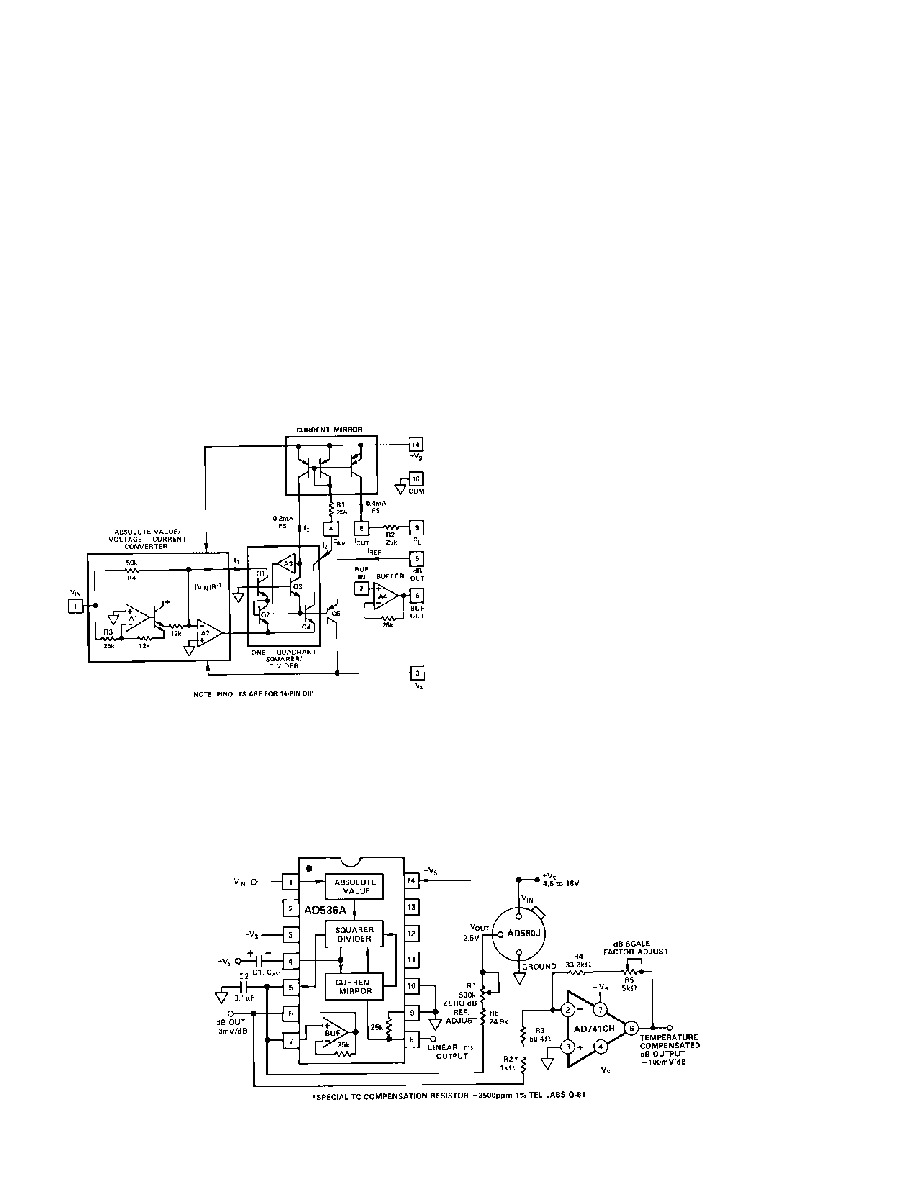
REV. B
AD536A
≠6≠
Figure 9 is a simplified schematic of the AD536A; it is subdi-
vided into four major sections: absolute value circuit (active
rectifier), squarer/divider, current mirror, and buffer amplifier.
The input voltage, V
IN
, which can be ac or dc, is converted to a
unipolar current I
1
, by the active rectifier A
1
, A
2
. I
1
drives one
input of the squarer/divider, which has the transfer function:
I
4
= I
1
2
/
I
3
The output current, I
4
, of the squarer/divider drives the current
mirror through a low-pass filter formed by R1 and the externally
connected capacitor, C
AV
. If the R1, C
AV
time constant is much
greater than the longest period of the input signal, then I
4
is
effectively averaged. The current mirror returns a current I
3
,
which equals Avg. [I
4
], back to the squarer/divider to complete
the implicit rms computation. Thus:
I
4
= Avg. I
1
2
/
I
4
[
]
= I
1
rms
Figure 9. Simplified Schematic
The current mirror also produces the output current, I
OUT,
which equals 2I
4
. I
OUT
can be used directly or converted to a
voltage with R2 and buffered by A4 to provide a low impedance
voltage output. The transfer function of the AD536A thus
results:
V
OUT
= 2R2 I rms = V
IN
rms
The dB output is derived from the emitter of Q3, since the
voltage at this point is proportional to ≠log V
IN
. Emitter fol-
lower, Q5, buffers and level shifts this voltage, so that the dB
output voltage is zero when the externally supplied emitter
current (I
REF
) to Q5 approximates I
3
.
CONNECTIONS FOR dB OPERATION
A powerful feature added to the AD536A is the logarithmic or
decibel output. The internal circuit computing dB works accu-
rately over a 60 dB range. The connections for dB measure-
ments are shown in Figure 10. The user selects the 0 dB level by
adjusting R1, for the proper 0 dB reference current (which is set
to exactly cancel the log output current from the squarer-divider
at the desired 0 dB point). The external op amp is used to pro-
vide a more convenient scale and to allow compensation of the
+0.33%/
∞C scale factor drift of the dB output pin. The special
T.C. resistor, R2, is available from Tel Labs in Londonderry,
N.H. (model Q-81) or from Precision Resistor Inc., Hillside,
N.J. (model PT146). The averaged temperature coefficients of
resistors R2 and R3 develop the +3300 ppm needed to reverse
compensate the dB output. The linear rms output is available at
Pin 8 on DIP or Pin 10 on header device with an output imped-
ance of 25 k
; thus some applications may require an additional
buffer amplifier if this output is desired.
dB Calibration:
1. Set V
IN
= 1.00 V dc or 1.00 V rms
2. Adjust R1 for dB out = 0.00 V
3. Set V
IN
= +0.1 V dc or 0.10 V rms
4. Adjust R5 for dB out = ≠2.00 V
Any other desired 0 dB reference level can be used by setting
V
IN
and adjusting R1, accordingly. Note that adjusting R5 for
the proper gain automatically gives the correct temperature
compensation.
Figure 10. dB Connection
REV. B
AD536A
≠7≠
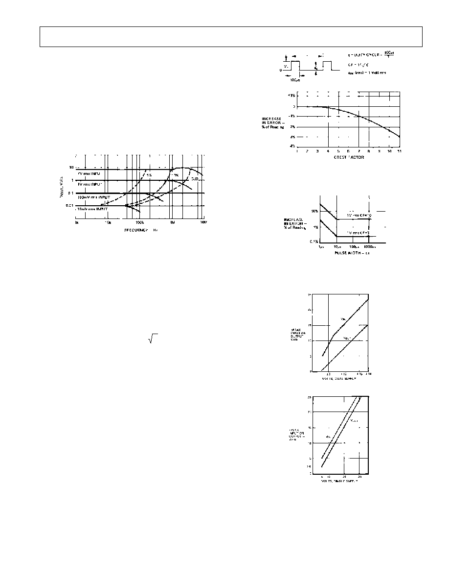
FREQUENCY RESPONSE
The AD536A utilizes a logarithmic circuit in performing the
implicit rms computation. As with any log circuit, bandwidth is
proportional to signal level. The solid lines in the graph below
represent the frequency response of the AD536A at input levels
from 10 millivolts to 7 volts rms. The dashed lines indicate the
upper frequency limits for 1%, 10%, and 3 dB of reading addi-
tional error. For example, note that a 1 volt rms signal will pro-
duce less than 1% of reading additional error up to 120 kHz. A
10 millivolt signal can be measured with 1% of reading addi-
tional error (100
µV) up to only 5 kHz.
Figure 11. High Frequency Response
AC MEASUREMENT ACCURACY AND CREST FACTOR
Crest factor is often overlooked in determining the accuracy of
an ac measurement. Crest factor is defined as the ratio of the
peak signal amplitude to the rms value of the signal (CF = V
P
/
V rms). Most common waveforms, such as sine and triangle
waves, have relatively low crest factors (<2). Waveforms which
resemble low duty cycle pulse trains, such as those occurring in
switching power supplies and SCR circuits, have high crest
factors. For example, a rectangular pulse train with a 1% duty
cycle has a crest factor of 10 (CF = 1
).
Figure 12 is a curve of reading error for the AD536A for a 1 volt
rms input signal with crest factors from 1 to 11. A rectangular
pulse train (pulsewidth 100
µs) was used for this test since it is
the worst-case waveform for rms measurement (all the energy is
contained in the peaks). The duty cycle and peak amplitude
were varied to produce crest factors from 1 to 11 while main-
taining a constant 1 volt rms input amplitude.
Figure 12. Error vs. Crest Factor
Figure 13. AD536A Error vs. Pulsewidth Rectangular
Pulse
Figure 14. AD536A Input and Output Voltage Ranges
vs. Supply
REV. B
AD536A
≠8≠
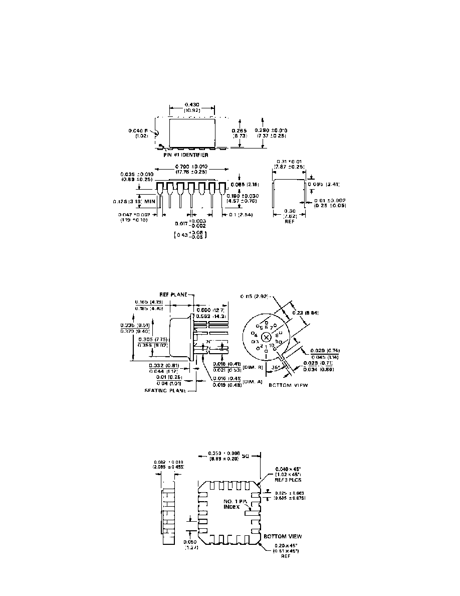
OUTLINE DIMENSIONS
Dimensions shown in inches and (mm).
C502e
≠
0
≠
6/99
PRINTED IN U.S.A.
D-14 Package
TO-116
E-20A Package
LCC
H-10A Package
TO-100