
REV. C
Information furnished by Analog Devices is believed to be accurate and
reliable. However, no responsibility is assumed by Analog Devices for its
use, nor for any infringements of patents or other rights of third parties
which may result from its use. No license is granted by implication or
otherwise under any patent or patent rights of Analog Devices.
a
AD8001
One Technology Way, P.O. Box 9106, Norwood, MA 02062-9106, U.S.A.
Tel: 781/329-4700
World Wide Web Site: http://www.analog.com
Fax: 781/326-8703
© Analog Devices, Inc., 1999
800 MHz, 50 mW
Current Feedback Amplifier
FEATURES
Excellent Video Specifications (R
L
= 150 , G = +2)
Gain Flatness 0.1 dB to 100 MHz
0.01% Differential Gain Error
0.025 Differential Phase Error
Low Power
5.5 mA Max Power Supply Current (55 mW)
High Speed and Fast Settling
880 MHz, ≠3 dB Bandwidth (G = +1)
440 MHz, ≠3 dB Bandwidth (G = +2)
1200 V/ s Slew Rate
10 ns Settling Time to 0.1%
Low Distortion
≠65 dBc THD, f
C
= 5 MHz
33 dBm 3rd Order Intercept, F
1
= 10 MHz
≠66 dB SFDR, f = 5 MHz
High Output Drive
70 mA Output Current
Drives Up to Four Back-Terminated Loads (75
Each)
While Maintaining Good Differential Gain/Phase
Performance (0.05%/0.25 )
APPLICATIONS
A-to-D Driver
Video Line Driver
Professional Cameras
Video Switchers
Special Effects
RF Receivers
FUNCTIONAL BLOCK DIAGRAMS
8-Lead DIP (N-8, Q-8)
5-Lead
and SOIC (SO-8)
SOT-23-5
1
2
3
4
8
7
6
5
AD8001
NC
NC
≠IN
NC
+IN
NC = NO CONNECT
OUT
V≠
V+
1
V
OUT
AD8001
≠V
S
+IN
2
3
4
5
+V
S
≠IN
PRODUCT DESCRIPTION
The AD8001 is a low power, high-speed amplifier designed
to operate on
±
5 V supplies. The AD8001 features unique
GAIN ≠ dB
9
6
≠12
10M
100M
1G
3
0
≠3
≠6
≠9
FREQUENCY ≠ Hz
V
S
= 5V
R
FB
= 820
V
S
= 5V
R
FB
= 1k
G = +2
R
L
= 100
Figure 1. Frequency Response of AD8001
transimpedance linearization circuitry. This allows it to drive
video loads with excellent differential gain and phase perfor-
mance on only 50 mW of power. The AD8001 is a current
feedback amplifier and features gain flatness of 0.1 dB to 100 MHz
while offering differential gain and phase error of 0.01% and
0.025
∞
. This makes the AD8001 ideal for professional video
electronics such as cameras and video switchers. Additionally,
the AD8001's low distortion and fast settling make it ideal for
buffer high-speed A-to-D converters.
The AD8001 offers low power of 5.5 mA max (V
S
=
±
5 V) and
can run on a single +12 V power supply, while being capable of
delivering over 70 mA of load current. These features make this
amplifier ideal for portable and battery-powered applications
where size and power are critical.
The outstanding bandwidth of 800 MHz along with 1200 V/
µ
s
of slew rate make the AD8001 useful in many general purpose
high-speed applications where dual power supplies of up to
±
6 V
and single supplies from 6 V to 12 V are needed. The AD8001 is
available in the industrial temperature range of ≠40
∞
C to +85
∞
C.
Figure 2. Transient Response of AD8001; 2 V Step, G = +2

REV. C
≠2≠
AD8001≠SPECIFICATIONS
(@ T
A
= + 25 C, V
S
= 5 V, R
L
= 100
, unless otherwise noted)
Model
AD8001A
Conditions
Min
Typ
Max
Units
DYNAMIC PERFORMANCE
≠3 dB Small Signal Bandwidth,
N Package
G = +2, < 0.1 dB Peaking, R
F
= 750
350
440
MHz
G = +1, < 1 dB Peaking, R
F
= 1 k
650
880
MHz
R Package
G = +2, < 0.1 dB Peaking, R
F
= 681
350
440
MHz
G = +1, < 0.1 dB Peaking, R
F
= 845
575
715
MHz
RT Package
G = +2, < 0.1 dB Peaking, R
F
= 768
300
380
MHz
G = +1, < 0.1 dB Peaking, R
F
= 1 k
575
795
MHz
Bandwidth for 0.1 dB Flatness
N Package
G = +2, R
F
= 750
85
110
MHz
R Package
G = +2, R
F
= 681
100
125
MHz
RT Package
G = +2, R
F
= 768
120
145
MHz
Slew Rate
G = +2, V
O
= 2 V Step
800
1000
V/
µ
s
G = ≠1, V
O
= 2 V Step
960
1200
V/
µ
s
Settling Time to 0.1%
G = ≠1, V
O
= 2 V Step
10
ns
Rise and Fall Time
G = +2, V
O
= 2 V Step, R
F
= 649
1.4
ns
NOISE/HARMONIC PERFORMANCE
Total Harmonic Distortion
f
C
= 5 MHz, V
O
= 2 V p-p
≠65
dBc
G = +2, R
L
= 100
Input Voltage Noise
f = 10 kHz
2.0
nV/
Hz
Input Current Noise
f = 10 kHz, +In
2.0
pA/
Hz
≠In
18
pA/
Hz
Differential Gain Error
NTSC, G = +2, R
L
= 150
0.01
0.025
%
Differential Phase Error
NTSC, G = +2, R
L
= 150
0.025
0.04
Degree
Third Order Intercept
f = 10 MHz
33
dBm
1 dB Gain Compression
f = 10 MHz
14
dBm
SFDR
f = 5 MHz
≠66
dB
DC PERFORMANCE
Input Offset Voltage
2.0
5.5
mV
T
MIN
≠T
MAX
2.0
9.0
mV
Offset Drift
10
µ
V/
∞
C
≠Input Bias Current
5.0
25
±µ
A
T
MIN
≠T
MAX
35
±µ
A
+Input Bias Current
3.0
6.0
±µ
A
T
MIN
≠T
MAX
10
±µ
A
Open Loop Transresistance
V
O
=
±
2.5 V
250
900
k
T
MIN
≠T
MAX
175
k
INPUT CHARACTERISTICS
Input Resistance
+Input
10
M
≠Input
50
Input Capacitance
+Input
1.5
pF
Input Common-Mode Voltage Range
3.2
±
V
Common-Mode Rejection Ratio
Offset Voltage
V
CM
=
±
2.5 V
50
54
dB
≠Input Current
V
CM
=
±
2.5 V, T
MIN
≠T
MAX
0.3
1.0
µ
A/V
+Input Current
V
CM
=
±
2.5 V, T
MIN
≠T
MAX
0.2
0.7
µ
A/V
OUTPUT CHARACTERISTICS
Output Voltage Swing
R
L
= 150
2.7
3.1
±
V
Output Current
R
L
= 37.5
50
70
mA
Short Circuit Current
85
110
mA
POWER SUPPLY
Operating Range
±
3.0
±
6.0
V
Quiescent Current
T
MIN
≠T
MAX
5.0
5.5
mA
Power Supply Rejection Ratio
+V
S
= +4 V to +6 V, ≠V
S
= ≠5 V
60
75
dB
≠V
S
= ≠ 4 V to ≠ 6 V, +V
S
= +5 V
50
56
dB
≠Input Current
T
MIN
≠T
MAX
0.5
2.5
µ
A/V
+Input Current
T
MIN
≠T
MAX
0.1
0.5
µ
A/V
Specifications subject to change without notice.
REV. C
AD8001
≠3≠
ABSOLUTE MAXIMUM RATINGS
1
Supply Voltage . . . . . . . . . . . . . . . . . . . . . . . . . . . . . . . . 12.6 V
Internal Power Dissipation
2
Plastic DIP Package (N) . . . . . . . . . . . . . . . . . . . . . . . 1.3 W
Small Outline Package (R) . . . . . . . . . . . . . . . . . . . . . . 0.9 W
SOT-23-5 Package (RT) . . . . . . . . . . . . . . . . . . . . . . . 0.5 W
Input Voltage (Common Mode) . . . . . . . . . . . . . . . . . . . .
±
V
S
Differential Input Voltage . . . . . . . . . . . . . . . . . . . . . . .
±
1.2 V
Output Short Circuit Duration
. . . . . . . . . . . . . . . . . . . . . . Observe Power Derating Curves
Storage Temperature Range N, R . . . . . . . . . ≠65
∞
C to +125
∞
C
Operating Temperature Range (A Grade) . . . ≠40
∞
C to +85
∞
C
Lead Temperature Range (Soldering 10 sec) . . . . . . . . +300
∞
C
NOTES
1
Stresses above those listed under Absolute Maximum Ratings may cause perma-
nent damage to the device. This is a stress rating only; functional operation of the
device at these or any other conditions above those indicated in the operational
section of this specification is not implied. Exposure to absolute maximum rating
conditions for extended periods may affect device reliability.
2
Specification is for device in free air:
8-Lead Plastic DIP Package:
JA
= 90
∞
C/W
8-Lead SOIC Package:
JA
= 155
∞
C/W
8-Lead Cerdip Package:
JA
= 110
∞
C/W
5-Lead SOT-23-5 Package:
JA
= 260
∞
C/W
MAXIMUM POWER DISSIPATION
The maximum power that can be safely dissipated by the
AD8001 is limited by the associated rise in junction tempera-
ture. The maximum safe junction temperature for plastic
encapsulated devices is determined by the glass transition tem-
perature of the plastic, approximately +150
∞
C. Exceeding this
limit temporarily may cause a shift in parametric performance
due to a change in the stresses exerted on the die by the package.
Exceeding a junction temperature of +175
∞
C for an extended
period can result in device failure.
While the AD8001 is internally short circuit protected, this
may not be sufficient to guarantee that the maximum junction
temperature (+150
∞
C) is not exceeded under all conditions. To
ensure proper operation, it is necessary to observe the maximum
power derating curves.
2.0
0
≠50
80
1.5
0.5
≠40
1.0
0
10
≠10
≠20
≠30
20
30
40
50
60
70
90
AMBIENT TEMPERATURE ≠ C
MAXIMUM POWER DISSIPATION ≠ Watts
8-LEAD
PLASTIC DIP PACKAGE
8-LEAD
SOIC PACKAGE
T
J
= +150 C
5-LEAD
SOT-23-5 PACKAGE
Figure 3. Plot of Maximum Power Dissipation vs.
Temperature
CAUTION
ESD (electrostatic discharge) sensitive device. Electrostatic charges as high as 4000 V readily
accumulate on the human body and test equipment and can discharge without detection.
Although the AD8001 features proprietary ESD protection circuitry, permanent damage may
occur on devices subjected to high energy electrostatic discharges. Therefore, proper ESD
precautions are recommended to avoid performance degradation or loss of functionality.
WARNING!
ESD SENSITIVE DEVICE
ORDERING GUIDE
Temperature
Package
Package
Brand
Model
Range
Description
Option
Code
AD8001AN
≠40
∞
C to +85
∞
C
8-Lead Plastic DIP
N-8
AD8001AQ
≠55
∞
C to +125
∞
C
8-Lead Cerdip
Q-8
AD8001AR
≠40
∞
C to +85
∞
C
8-Lead SOIC
SO-8
AD8001AR-REEL
≠40
∞
C to +85
∞
C
13" Tape and REEL
SO-8
AD8001AR-REEL7
≠40
∞
C to +85
∞
C
7" Tape and REEL
SO-8
AD8001ART-REEL
≠40
∞
C to +85
∞
C
13" Tape and REEL
RT-5
HEA
AD8001ART-REEL7
≠40
∞
C to +85
∞
C
7" Tape and REEL
RT-5
HEA
AD8001ACHIPS
≠40
∞
C to +85
∞
C
Die Form
5962-9459301MPA
1
≠55
∞
C to +125
∞
C
8-Lead Cerdip
Q-8
AD8001R-EB+2
2
SOIC Evaluation Board, G = +2
NOTES
1
Standard Military Drawing Device.
2
Refer to Evaluation Board section.
REV. C
AD8001
≠4≠
HP8133A
PULSE
GENERATOR
806
+V
S
R
L
= 100
50
V
IN
0.1 F
0.001 F
AD8001
0.1 F
0.001 F
T
R
/T
F
= 50ps
806
V
OUT
TO
TEKTRONIX
CSA 404 COMM.
SIGNAL
ANALYZER
≠V
S
Figure 4. Test Circuit , Gain = +2
Figure 5. 1 V Step Response, G = +2
0.5V
5ns
Figure 6. 2 V Step Response, G = +1
5ns
400mV
Figure 7. 2 V Step Response, G = +2
LeCROY 9210
PULSE
GENERATOR
909
+V
S
R
L
= 100
≠V
S
50
V
IN
0.1 F
0.001 F
AD8001
0.1 F
0.001 F
T
R
/T
F
= 350ps
V
OUT
TO
TEKTRONIX
CSA 404 COMM.
SIGNAL
ANALYZER
Figure 8. Test Circuit, Gain = +1
Figure 9. 100 mV Step Response, G = +1
REV. C
AD8001
≠5≠
GAIN ≠ dB
9
6
≠12
10M
100M
1G
3
0
≠3
≠6
≠9
FREQUENCY ≠ Hz
V
S
= 5V
R
FB
= 820
V
S
= 5V
R
FB
= 1k
G = +2
R
L
= 100
Figure 10. Frequency Response, G = +2
OUTPUT ≠ dB
0.1
0
≠0.9
1M
10M
100M
≠0.1
≠0.2
≠0.3
≠0.4
≠0.5
FREQUENCY ≠ Hz
≠0.6
≠0.7
≠0.8
R
F
=
649
R
F
= 698
R
F
= 750
G = +2
R
L
= 100
V
IN
= 50mV
Figure 11. 0.1 dB Flatness, R Package (for N Package Add
50
to R
F
)
≠50
≠80
≠110
100k
100M
10M
1M
10k
≠90
≠100
≠70
≠60
FREQUENCY ≠ Hz
HARMONIC DISTORTION ≠ dBc
V
OUT
= 2V p-p
R
L
= 1k
G = +2
5V SUPPLIES
3RD HARMONIC
2ND HARMONIC
Figure 12. Distortion vs. Frequency, R
L
= 1 k
VALUE OF FEEDBACK RESISTOR (R
F
) ≠
≠3dB BANDWIDTH ≠ MHz
1000
0
1000
600
200
600
400
500
800
900
800
700
R
PACKAGE
N
PACKAGE
V
S
= 5V
R
L
= 100
G = +2
Figure 13. ≠3 dB Bandwidth vs. R
F
≠50
≠70
≠100
100k
100M
10M
1M
10k
≠80
≠90
≠60
FREQUENCY ≠ Hz
HARMONIC DISTORTION ≠ dBc
V
OUT
= 2V p-p
R
L
= 100
G = +2
5V SUPPLIES
2ND HARMONIC
3RD HARMONIC
Figure 14. Distortion vs. Frequency, R
L
= 100
0.08
0.01
≠0.01
0
0.00
0.00
0.02
0.02
0.04
0.06
100
IRE
DIFF GAIN ≠ %
DIFF PHASE ≠ Degrees
≠0.02
G = +2
R
F
= 806
1 BACK TERMINATED
LOAD (150 )
2 BACK TERMINATED
LOADS (75 )
1 AND 2 BACK TERMINATED
LOADS (150
AND 75 )
Figure 15. Differential Gain and Differential Phase

REV. C
AD8001
≠6≠
GAIN ≠ dB
0
≠5
≠35
100M
1G
3G
≠10
≠15
≠20
≠25
≠30
FREQUENCY ≠ Hz
5
V
IN
= ≠26dBm
R
F
= 909
Figure 16. Frequency Response, G = +1
+1
≠4
≠9
10M
1G
100M
2M
≠3
≠2
≠1
0
≠8
≠7
≠6
≠5
OUTPUT ≠ dB
FREQUENCY ≠ Hz
G = +1
R
L
= 100
V
IN
= 50mV
R
F
= 649
R
F
= 953
Figure 17. Flatness, R Package, G = +1 (for N Package Add
100
to R
F
)
≠40
≠60
≠110
100k
100M
10M
1M
10k
≠50
≠80
≠70
≠100
≠90
DISTORTION ≠ dBc
FREQUENCY ≠ Hz
G = +1
R
L
= 1k
V
OUT
= 2V p-p
2ND
HARMONIC
3RD
HARMONIC
Figure 18. Distortion vs. Frequency, R
L
= 1 k
1000
900
500
600
700
1100
800
900
800
700
600
1000
VALUE OF FEEDBACK RESISTOR (RF) ≠
≠3dB BANDWIDTH ≠ MHz
N PACKAGE
R PACKAGE
V
IN
= 50mV
R
L
= 100
G = +1
Figure 19. ≠3 dB Bandwidth vs. R
F
, G = +1
FREQUENCY ≠ Hz
10k
100k
1M
10M
100M
≠40
≠70
≠100
≠80
≠90
≠60
≠50
DISTORTION ≠ dBc
R
L
= 100
G = +1
V
OUT
= 2V p-p
2ND HARMONIC
3RD HARMONIC
Figure 20. Distortion vs. Frequency, R
L
= 100
3
≠9
≠24
1M
100M
10M
≠12
≠15
≠6
≠3
FREQUENCY ≠ Hz
≠27
0
≠18
≠21
OUTPUT ≠ dBV
R
L
= 100
G = +1
Figure 21. Large Signal Frequency Response, G = +1

REV. C
AD8001
≠7≠
25
10
≠5
1M
10M
100M
0
5
15
20
FREQUENCY ≠ Hz
GAIN ≠ dB
≠25
≠20
≠15
≠10
1G
45
30
35
40
R
F
= 470
G = +100
G = +10
R
L
= 100
R
F
= 1000
Figure 22. Frequency Response, G = +10, G = +100
3.35
100
2.95
≠40
≠60
3.05
3.15
3.25
80
60
40
20
0
≠20
OUTPUT SWING ≠ Volts
JUNCTION TEMPERATURE ≠ C
2.75
2.85
2.55
2.65
R
L
= 50
V
S
= 5V
R
L
= 150
V
S
= 5V
|
≠V
OUT
|
|
≠V
OUT
|
+V
OUT
+V
OUT
Figure 23. Output Swing vs. Temperature
≠60
JUNCTION TEMPERATURE ≠ C
INPUT BIAS CURRENT
≠
A
≠4
2
≠2
1
0
5
≠3
≠40
≠20
0
20
40
60
80
100
120
140
≠1
3
4
+IN
≠IN
Figure 24. Input Bias Current vs. Temperature
2.2
0.4
100
0.8
0.6
≠40
≠60
1.0
1.2
1.4
1.6
1.8
2.0
80
60
40
20
0
≠20
INPUT OFFSET VOLTAGE ≠ mV
JUNCTION TEMPERATURE ≠ C
DEVICE #1
DEVICE #2
DEVICE #3
Figure 25. Input Offset vs. Temperature
≠60
JUNCTION TEMPERATURE ≠ C
SUPPLY CURRENT
≠ mA
4.4
4.8
5.8
≠40
≠20
0
20
40
60
80
100
120
140
5.2
5.4
4.6
5.6
5.0
V
S
= 5V
Figure 26. Supply Current vs. Temperature
125
85
100
95
90
≠40
≠60
105
100
110
115
120
80
60
40
20
0
≠20
JUNCTION TEMPERATURE ≠ C
SHORT CIRCUIT CURRENT ≠ mA
SOURCE I
SC
|
SINK I
SC
|
Figure 27. Short Circuit Current vs. Temperature
REV. C
AD8001
≠8≠
≠60
JUNCTION TEMPERATURE ≠ C
TRANSRESISTANCE
≠ k
0
1
6
≠40
≠20
0
20
40
60
80
100
120
140
3
4
5
2
V
S
= 5V
R
L
= 150
V
OUT
= 2.5V
≠T
Z
+T
Z
Figure 28. Transresistance vs. Temperature
100
10
1
10
100
10k
1k
FREQUENCY ≠ Hz
100
10
1
NOISE VOLTAGE ≠ nV/
Hz
NOISE CURRENT ≠ pA/
Hz
100k
INVERTING CURRENT V
S
= 5V
NONINVERTING CURRENT V
S
= 5V
VOLTAGE NOISE V
S
= 5V
Figure 29. Noise vs. Frequency
≠60
JUNCTION TEMPERATURE ≠ C
CMRR
≠ dB
≠48
≠40
≠20
0
20
40
60
80
100
120
140
≠51
≠50
≠49
≠53
≠55
≠54
≠52
≠56
+CMRR
≠CMRR
2.5V SPAN
Figure 30. CMRR vs. Temperature
100k
100M
10M
1M
10k
0.01
1k
10
0.1
100
FREQUENCY ≠ Hz
R
OUT
≠
1
G = +2
R
F
= 909
Figure 31. Output Resistance vs. Frequency
1
≠4
≠9
1M
10M
1G
100M
≠5
≠6
≠7
≠8
≠3
≠2
≠1
0
FREQUENCY ≠ Hz
OUTPUT ≠ dB
G = ≠1
R
L
= 100
V
IN
= 50mV
R
F
= 576
R
F
= 649
R
F
= 750
Figure 32. ≠3 dB Bandwidth vs. Frequency, G = ≠1
≠60
JUNCTION TEMPERATURE ≠ C
PSRR
≠ dB
≠52.5
≠40
≠20
0
20
40
60
80
100
≠62.5
≠60.0
≠57.5
≠67.5
≠75.0
≠72.5
≠65.0
≠77.5
≠70.0
≠55.0
+PSRR
≠PSRR
3V SPAN
CURVES ARE FOR WORST
CASE CONDITION WHERE
ONE SUPPLY IS VARIED
WHILE THE OTHER IS
HELD CONSTANT.
Figure 33. PSRR vs. Temperature

REV. C
AD8001
≠9≠
300k
100M
10M
1M
FREQUENCY ≠ Hz
≠20
≠10
≠40
≠30
CMRR ≠ dB
910
V
OUT
V
IN
150
150
910
51
62
1G
≠50
Figure 34. CMRR vs. Frequency
1
≠4
≠9
1M
10M
1G
100M
≠5
≠6
≠7
≠8
≠3
≠2
≠1
0
FREQUENCY ≠ Hz
OUTPUT ≠ dB
R
F
= 750
R
F
= 649
R
F
= 549
G = ≠2
R
L
= 100
V
IN
= 50mV
rms
Figure 35. ≠3 dB Bandwidth vs. Frequency, G = ≠2
Figure 36. 100 mV Step Response, G = ≠1
10
≠20
1M
10M
100M
≠10
0
20
FREQUENCY ≠ Hz
PSRR ≠ dB
≠60
≠50
≠40
≠30
1G
30
CURVES ARE FOR WORST
CASE CONDITION WHERE
ONE SUPPLY IS VARIED
WHILE THE OTHER IS
HELD CONSTANT.
R
F
= 909
G = +2
≠PSRR
+PSRR
≠PSRR
+PSRR
Figure 37. PSRR vs. Frequency
Figure 38. 2 V Step Response, G = ≠1
3
≠4
≠5
2
1
0
≠1
≠2
≠3
5
4
100
20
0
10
80
90
70
60
50
40
30
100
20
0
10
80
90
70
60
50
40
30
COUNT
PERCENT
INPUT OFFSET VOLTAGE ≠ mV
3 WAFER LOTS
COUNT = 895
MEAN = 1.37
STD DEV = 1.13
MIN = ≠2.45
MAX = +4.69
FREQ DIST
CUMULATIVE
Figure 39. Input Offset Voltage Distribution

REV. C
AD8001
≠10≠
THEORY OF OPERATION
A very simple analysis can put the operation of the AD8001, a
current feedback amplifier, in familiar terms. Being a current
feedback amplifier, the AD8001's open-loop behavior is ex-
pressed as transimpedance,
V
O
/
I
≠IN
, or T
Z
. The open-loop
transimpedance behaves just as the open-loop voltage gain of a
voltage feedback amplifier, that is, it has a large dc value and
decreases at roughly 6 dB/octave in frequency.
Since the R
IN
is proportional to 1/g
M
, the equivalent voltage
gain is just T
Z
◊
g
M
, where the g
M
in question is the trans-
conductance of the input stage. This results in a low open-loop
input impedance at the inverting input, a now familiar result.
Using this amplifier as a follower with gain, Figure 40, basic
analysis yields the following result.
V
V
G
T
S
T
S
G
R
R
G
R
R
R
g
O
IN
Z
Z
IN
IN
M
=
◊
+
◊
+
= +
=
( )
( )
/
1
1
1
2
1
50
Recognizing that G
◊
R
IN
<< R1 for low gains, it can be seen to
the first order that bandwidth for this amplifier is independent
of gain (G). This simple analysis in conjunction with Figure 41
can, in fact, predict the behavior of the AD8001 over a wide
range of conditions.
V
OUT
R1
R2
R
IN
V
IN
Figure 40.
Considering that additional poles contribute excess phase at
high frequencies, there is a minimum feedback resistance below
which peaking or oscillation may result. This fact is used to
determine the optimum feedback resistance, R
F
. In practice
parasitic capacitance at Pin 2 will also add phase in the feedback
loop, so picking an optimum value for R
F
can be difficult. Fig-
ure 42 illustrates this problem. Here the fine scale (0.1 dB/div)
flatness is plotted vs feedback resistance. These plots were taken
using an evaluation card which is available to customers so that
these results may readily be duplicated (see Evaluation Board
section).
Achieving and maintaining gain flatness of better than 0.1 dB at
frequencies above 10 MHz requires careful consideration of
several issues.
FREQUENCY ≠ Hz
1M
10
100k
1M
1G
100M
10M
100
100k
10k
1k
T
Z
≠
Figure 41. Transimpedance vs. Frequency
OUTPUT ≠ dB
0.1
0
≠0.9
1M
10M
100M
≠0.1
≠0.2
≠0.3
≠0.4
≠0.5
FREQUENCY ≠ Hz
≠0.6
≠0.7
≠0.8
G = +2
R
F
=
649
R
F
= 698
R
F
= 750
Figure 42. 0.1 dB Flatness vs. Frequency
Choice of Feedback and Gain Resistors
Because of the above-mentioned relationship between the band-
width and feedback resistor, the fine scale gain flatness will, to
some extent, vary with feedback resistance. It, therefore, is
recommended that once optimum resistor values have been
determined, 1% tolerance values should be used if it is desired
to maintain flatness over a wide range of production lots. In
addition, resistors of different construction have different associ-
ated parasitic capacitance and inductance. Surface mount resis-
tors were used for the bulk of the characterization for this data
sheet. It is not recommended that leaded components be used
with the AD8001.
REV. C
AD8001
≠11≠
Printed Circuit Board Layout Considerations
As to be expected for a wideband amplifier, PC board parasitics
can affect the overall closed-loop performance. Of concern are
stray capacitances at the output and the inverting input nodes. If
a ground plane is to be used on the same side of the board as
the signal traces, a space (5 mm min) should be left around the
signal lines to minimize coupling. Additionally, signal lines
connecting the feedback and gain resistors should be short
enough so that their associated inductance does not cause high
frequency gain errors. Line lengths on the order of less than
5 mm are recommended. If long runs of coaxial cable are being
driven, dispersion and loss must be considered.
Power Supply Bypassing
Adequate power supply bypassing can be critical when optimiz-
ing the performance of a high frequency circuit. Inductance in
the power supply leads can form resonant circuits that produce
peaking in the amplifier's response. In addition, if large current
transients must be delivered to the load, then bypass capacitors
(typically greater than 1
µ
F) will be required to provide the best
settling time and lowest distortion. A parallel combination of
4.7
µ
F and 0.1
µ
F is recommended. Some brands of electrolytic
capacitors will require a small series damping resistor
4.7
for
optimum results.
DC Errors and Noise
There are three major noise and offset terms to consider in a
current feedback amplifier. For offset errors refer to the equa-
tion below. For noise error the terms are root-sum-squared to
give a net output error. In the circuit below (Figure 43) they are
input offset (V
IO
) which appears at the output multiplied by the
noise gain of the circuit (1 + R
F
/R
I
), noninverting input current
(I
BN
◊
R
N
) also multiplied by the noise gain, and the inverting
input current, which when divided between R
F
and R
I
and sub-
sequently multiplied by the noise gain always appears at the
output as I
BN
◊
R
F
. The input voltage noise of the AD8001 is a
low 2 nV/
Hz. At low gains though the inverting input current
noise times R
F
is the dominant noise source. Careful layout and
device matching contribute to better offset and drift specifica-
tions for the AD8001 compared to many other current feedback
amplifiers. The typical performance curves in conjunction with
the equations below can be used to predict the performance of
the AD8001 in any application.
V
V
R
R
I
R
R
R
I
R
OUT
IO
F
I
BN
N
F
I
BI
F
=
◊
+
±
◊
◊
+
±
◊
1
1
R
F
R
I
R
N
I
BN
V
OUT
I
BI
Figure 43. Output Offset Voltage
Driving Capacitive Loads
The AD8001 was designed primarily to drive nonreactive loads.
If driving loads with a capacitive component is desired, best
frequency response is obtained by the addition of a small series
resistance as shown in Figure 44. The accompanying graph
shows the optimum value for R
SERIES
vs. capacitive load. It is
worth noting that the frequency response of the circuit when
driving large capacitive loads will be dominated by the passive
roll-off of R
SERIES
and C
L
.
909
R
SERIES
R
L
500
I
N
C
L
Figure 44. Driving Capacitive Loads
40
0
0
25
30
10
5
20
15
20
10
C
L
≠ pF
G = +1
R
SERIES
≠
Figure 45. Recommended R
SERIES
vs. Capacitive Load
REV. C
AD8001
≠12≠
Communications
Distortion is a key specification in communications applications.
Intermodulation distortion (IMD) is a measure of the ability of
an amplifier to pass complex signals without the generation of
spurious harmonics. The third order products are usually the
most problematic since several of them fall near the fundamen-
tals and do not lend themselves to filtering. Theory predicts that
the third order harmonic distortion components increase in
power at three times the rate of the fundamental tones. The
specification of third order intercept as the virtual point where
fundamental and harmonic power are equal is one standard
measure of distortion performance. Op amps used in closed-
loop applications do not always obey this simple theory. At a
gain of two, the AD8001 has performance summarized in Fig-
ure 46. Here the worst third order products are plotted vs. input
power. The third order intercept of the AD8001 is +33 dBm at
10 MHz.
≠80
3
≠7
≠75
2
1
0
≠4
≠5
6
≠2
≠70
≠65
≠60
≠55
≠50
≠45
≠1
THIRD ORDER IMD ≠ dBc
INPUT POWER ≠ dBm
≠6
≠8
4
5
≠3
2F
2
≠ F
1
2F
1
≠ F
2
G = +2
F
1
= 10MHz
F
2
= 12MHz
Figure 46. Third Order IMD; F
1
= 10 MHz, F
2
= 12 MHz
Operation as a Video Line Driver
The AD8001 has been designed to offer outstanding perfor-
mance as a video line driver. The important specifications of
differential gain (0.01%) and differential phase (0.025
∞
) meet
the most exacting HDTV demands for driving one video load.
The AD8001 also drives up to two back terminated loads as
shown in Figure 47, with equally impressive performance (0.01%,
0.07
∞
). Another important consideration is isolation between
loads in a multiple load application. The AD8001 has more
than 40 dB of isolation at 5 MHz when driving two 75
back
terminated loads.
909
909
75
CABLE
75
75
V
OUT
#1
V
OUT
#2
+V
S
≠V
S
V
IN
0.1 F
0.001 F
AD8001
0.1 F
75
CABLE
75
75
75
CABLE
+
0.001 F
75
Figure 47. Video Line Driver

REV. C
AD8001
≠13≠
0.1 F
+V
S
≠V
S
20
50
1k
18
17
16
15
14
13
12
11
≠V
REF A
10pF
CLOCK
5, 9, 22,
24, 37, 41
4,19, 21 25, 27, 42
0.1 F
38
8
≠V
REF B
6
+V
INT
2
3
+V
REF A
A
IN A
649
324
ANALOG
IN A
0.5V
1.3k
AD707
43
+V
REF B
20k
0.1 F
≠2V
1.3k
20k
649
ANALOG
IN B
0.5V
324
20
0.1 F
40
COMP
1
A
IN B
ENCODE A
ENCODE B
10
36
ENCODE
74ACT04
0.1 F
+5V
28
29
30
31
32
33
34
35
RZ1
RZ2
D
0A
(LSB)
D
7A
(MSB)
D
0B
(LSB)
D
7B
(MSB)
7, 20,
26, 39
≠5V
1N4001
AD9058
(J-LEAD)
RZ1, RZ2 = 2,000 SIP (8-PKG)
74ACT 273
74ACT 273
8
8
AD8001
AD8001
Figure 48. AD8001 Driving a Dual A-to-D Converter
Driving A-to-D Converters
The AD8001 is well suited for driving high speed analog-to-
digital converters such as the AD9058. The AD9058 is a dual
8-bit 50 MSPS ADC. In the circuit below the AD8001 is shown
driving the inputs of the AD9058, which are configured for 0 V
to +2 V ranges. Bipolar input signals are buffered, amplified
(≠2
◊
), and offset (by +1.0 V) into the proper input range of the
ADC. Using the AD9058's internal +2 V reference connected
to both ADCs as shown in Figure 48 reduces the number of
external components required to create a complete data
acquisition system. The 20
resistors in series with ADC in-
puts are used to help the AD8001s drive the 10 pF ADC input
capacitance. The AD8001 only adds 100 mW to the power
consumption while not limiting the performance of the circuit.

REV. C
AD8001
≠14≠
Layout Considerations
The specified high speed performance of the AD8001 requires
careful attention to board layout and component selection.
Proper R
F
design techniques and low parasitic component selec-
tion are mandatory.
The PCB should have a ground plane covering all unused por-
tions of the component side of the board to provide a low im-
pedance ground path. The ground plane should be removed
from the area near the input pins to reduce stray capacitance.
Chip capacitors should be used for supply bypassing (see Figure
49). One end should be connected to the ground plane and the
other within 1/8-inch of each power pin. An additional large
(4.7
µ
F≠10
µ
F) tantalum electrolytic capacitor should be con-
nected in parallel, but not necessarily so close, to supply current
for fast, large-signal changes at the output.
The feedback resistor should be located close to the inverting
input pin in order to keep the stray capacitance at this node to a
minimum. Capacitance variations of less than 1 pF at the invert-
ing input will significantly affect high speed performance.
Stripline design techniques should be used for long signal traces
(greater than about 1 in.). These should be designed with a
characteristic impedance of 50
or 75
and be properly termi-
nated at each end.
Inverting Configuration
Supply Bypassing
C1
0.1 F
C2
0.1 F
+V
S
≠V
S
C3
10 F
C4
10 F
Noninverting Configuration
R
F
R
O
IN
+V
S
≠V
S
R
S
R
T
R
G
OUT
R
F
R
O
IN
+V
S
≠V
S
R
T
R
G
OUT
Figure 49. Inverting and Noninverting Configurations for Evaluation Boards
Table I. Recommended Component Values
AD8001AN (DIP)
AD8001AR (SOIC)
AD8001ART (SOT-23-5)
Gain
Gain
Gain
Component
≠1
+1
+2
+10
+100
≠1
+1
+2
+10
+100
≠1
+1
+2
+10
+100
R
F
(
)
649
1050
750
470
1000
604
953
681
470
1000
845
1000 768
470
1000
R
G
(
)
649
750
51
10
604
681
51
10
845
768
51
10
R
O
(Nominal) (
)
49.9
49.9
49.9
49.9
49.9
49.9
49.9
49.9
49.9
49.9
49.9
49.9
49.9
49.9
49.9
R
S
(
)
0
0
0
R
T
(Nominal) (
)
54.9
49.9
49.9
49.9
49.9
54.9
49.9
49.9
49.9
49.9
54.9
49.9
49.9
49.9
49.9
Small Signal
340
880
460
260
20
370
710
440
260
20
240
795
380
260
20
BW (MHz)
0.1 dB Flatness
105
70
105
130
100
120
110
300
145
(MHz)
REV. C
AD8001
≠15≠
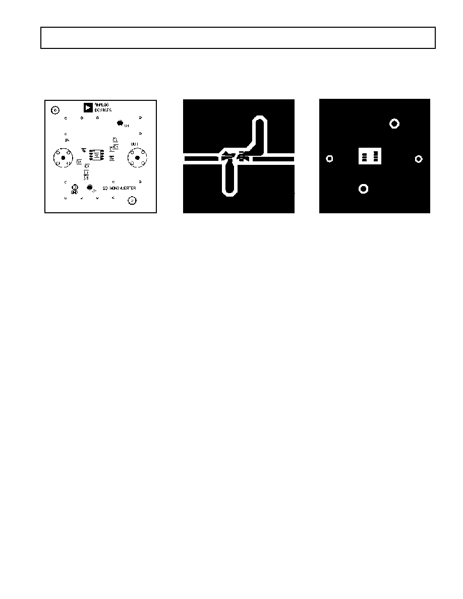
Figure 50. Evaluation Board
Silkscreen (Top)
Figure 51. Evaluation Board Layout
(Solder Side)
Figure 52. Evaluation Board Layout
(Component Side)
Evaluation Board
An evaluation board for the AD8001 is available that has been
carefully laid-out and tested to demonstrate that the specified
high speed performance of the device can be realized. For
ordering information, please refer to the Ordering Guide. The
layout of the evaluation board can be used as shown or serve as
a guide for a board layout.

REV. C
AD8001
≠16≠
C1886c≠0≠12/99
PRINTED IN U.S.A.
8-Lead Plastic DIP
(N-8)
SEATING
PLANE
0.060 (1.52)
0.015 (0.38)
0.210
(5.33)
MAX
0.022 (0.558)
0.014 (0.356)
0.160 (4.06)
0.115 (2.93)
0.070 (1.77)
0.045 (1.15)
0.130
(3.30)
MIN
8
1
4
5
PIN 1
0.280 (7.11)
0.240 (6.10)
0.100 (2.54)
BSC
0.430 (10.92)
0.348 (8.84)
0.195 (4.95)
0.115 (2.93)
0.015 (0.381)
0.008 (0.204)
0.325 (8.25)
0.300 (7.62)
8-Lead Plastic SOIC
(SO-8)
8
5
4
1
0.1968 (5.00)
0.1890 (4.80)
0.2440 (6.20)
0.2284 (5.80)
PIN 1
0.1574 (4.00)
0.1497 (3.80)
0.0500 (1.27)
BSC
0.0688 (1.75)
0.0532 (1.35)
SEATING
PLANE
0.0098 (0.25)
0.0040 (0.10)
0.0192 (0.49)
0.0138 (0.35)
0.0098 (0.25)
0.0075 (0.19)
0.0500 (1.27)
0.0160 (0.41)
8
0
0.0196 (0.50)
0.0099 (0.25)
45
OUTLINE DIMENSIONS
Dimensions shown in inches and (mm).
8-Lead Cerdip
(Q-8)
1
4
8
5
0.310 (7.87)
0.220 (5.59)
PIN 1
0.005 (0.13)
MIN
0.055 (1.4)
MAX
0.100 (2.54) BSC
15∞
0∞
0.320 (8.13)
0.290 (7.37)
0.015 (0.38)
0.008 (0.20)
SEATING
PLANE
0.200.(5.08)
MAX
0.405 (10.29) MAX
0.150
(3.81)
MIN
0.200 (5.08)
0.125 (3.18)
0.023 (0.58)
0.014 (0.36)
0.070 (1.78)
0.030 (0.76)
0.060 (1.52)
0.015 (0.38)
5-Lead Plastic Surface Mount (SOT-23)
(RT-5)
0.1181 (3.00)
0.1102 (2.80)
PIN 1
0.0669 (1.70)
0.0590 (1.50)
0.1181 (3.00)
0.1024 (2.60)
1
3
4
5
0.0748 (1.90)
BSC
0.0374 (0.95) BSC
2
0.0079 (0.20)
0.0031 (0.08)
0.0217 (0.55)
0.0138 (0.35)
10
0
0.0197 (0.50)
0.0138 (0.35)
0.0059 (0.15)
0.0019 (0.05)
0.0512 (1.30)
0.0354 (0.90)
SEATING
PLANE
0.0571 (1.45)
0.0374 (0.95)