REV. E
Information furnished by Analog Devices is believed to be accurate and
reliable. However, no responsibility is assumed by Analog Devices for its
use, nor for any infringements of patents or other rights of third parties
which may result from its use. No license is granted by implication or
otherwise under any patent or patent rights of Analog Devices.
a
AMP03
One Technology Way, P.O. Box 9106, Norwood, MA 02062-9106, U.S.A.
Tel: 781/329-4700
World Wide Web Site: http://www.analog.com
Fax: 781/326-8703
© Analog Devices, Inc., 1999
Precision, Unity-Gain
Differential Amplifier
FEATURES
High CMRR: 100 dB Typ
Low Nonlinearity: 0.001% Max
Low Distortion: 0.001% Typ
Wide Bandwidth: 3 MHz Typ
Fast Slew Rate: 9.5 V/ s Typ
Fast Settling (0.01%): 1
s Typ
Low Cost
APPLICATIONS
Summing Amplifiers
Instrumentation Amplifiers
Balanced Line Receivers
Current-Voltage Conversion
Absolute Value Amplifier
4 mA≠20 mA Current Transmitter
Precision Voltage Reference Applications
Lower Cost and Higher Speed Version of INA105
GENERAL DESCRIPTION
The AMP03 is a monolithic unity-gain, high speed differential
amplifier. Incorporating a matched thin-film resistor network,
the AMP03 features stable operation over temperature without
requiring expensive external matched components. The AMP03
is a basic analog building block for differential amplifier and
instrumentation applications.
The differential amplifier topology of the AMP03 serves to both
amplify the difference between two signals and provide extremely
high rejection of the common-mode input voltage. By providing
common-mode rejection (CMR) of 100 dB typical, the AMP03
solves common problems encountered in instrumentation design.
As an example, the AMP03 is ideal for performing either addi-
tion or subtraction of two signals without using expensive
externally-matched precision resistors. The large common-
mode rejection is made possible by matching the internal resistors
to better than 0.002% and maintaining a thermally symmetric
layout. Additionally, due to high CMR over frequency, the
AMP03 is an ideal general amplifier for buffering signals in a
noisy environment into data acquisition systems.
The AMP03 is a higher speed alternative to the INA105. Fea-
turing slew rates of 9.5 V/
µ
s, and a bandwidth of 3 MHz, the
AMP03 offers superior performance for high speed current
sources, absolute value amplifiers and summing amplifiers than
the INA105.
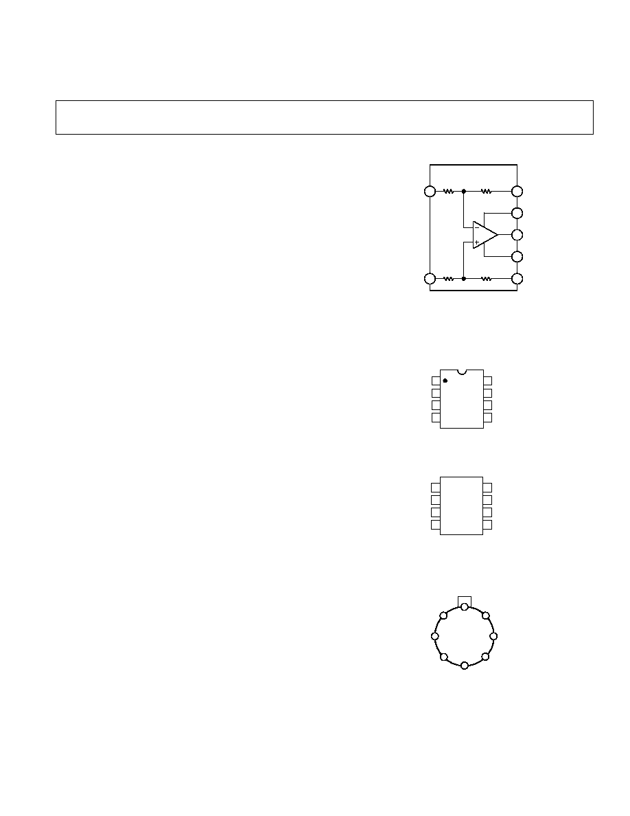
FUNCTIONAL BLOCK DIAGRAM
≠IN
+IN
SENSE
+V
CC
OUTPUT
≠V
EE
REFERENCE
25k
25k
25k
25k
6
7
1
2
3
4
5
AMP03
PIN CONNECTIONS
8-Lead Plastic DIP
(P Suffix)
1
2
3
4
8
7
6
5
TOP VIEW
(Not to Scale)
NC = NO CONNECT
AMP03
REFERENCE
SENSE
OUTPUT
V+
NC
≠IN
+IN
V≠
8-Lead SOIC
(S Suffix)
1
2
3
4
8
7
6
5
TOP VIEW
(Not to Scale)
NC = NO CONNECT
AMP03
REFERENCE
SENSE
OUTPUT
V+
NC
≠IN
+IN
V≠
Header
(J Suffix)
8
REFERENCE 1
≠IN 2
+IN 3
7 V+
6 OUTPUT
5 SENSE
4
V≠
NC
NC = NO CONNECT
≠2≠
REV. E
AMP03≠SPECIFICATIONS
ELECTRICAL CHARACTERISTICS
AMP03F
AMP03B
AMP03G
Parameter
Symbol Conditions
Min
Typ
Max
Min
Typ
Max
Min
Typ
Max
Units
Offset Voltage
V
OS
V
CM
= 0 V
≠400
10
400
≠700
20
700
≠750
25
750
µ
V
Gain Error
No Load, V
IN
=
±
10 V,
R
S
= 0
0.00004 0.008
0.00004 0.008
0.001 0.008
%
Input Voltage Range
IVR
(Note 1)
±
10
±
10
±
10
V
Common-Mode Rejection
CMR
V
CM
=
±
10 V
85
100
80
95
80
95
dB
Power Supply Rejection Ratio PSRR
V
S
=
±
6 V to
±
18 V
0.6
10
0.6
10
0.7
10
µ
V/V
Output Swing
V
O
R
L
= 2 k
±
12
±
13.7
±
12
±
13.7
±
12
±
13.7
V
Short-Circuit Current Limit
I
SC
Output Shorted
to Ground
+45/≠15
+45/≠15
+45/≠15
mA
Small-Signal Bandwidth
(≠3 dB)
BW
R
L
= 2 k
3
3
3
MHz
Slew Rate
SR
R
L
= 2 k
6
9.5
6
9.5
6
9.5
V/
µ
s
Capacitive Load Drive
Capability
C
L
No Oscillation
300
300
300
pF
Supply Current
I
SY
No Load
2.5
3.5
2.5
3.5
2.5
3.5
mA
NOTES
1
Input voltage range guaranteed by CMR test.
Specifications subject to change without notice.
ELECTRICAL CHARACTERISTICS
AMP03B
Parameter
Symbol
Conditions
Min
Typ
Max
Units
Offset Voltage
V
OS
V
CM
= 0 V
≠1500
150
1500
µ
V
Gain Error
No Load, V
IN
=
±
10 V, R
S
= 0
0.0014
0.02
%
Input Voltage Range
IVR
±
20
V
Common-Mode Rejection
CMR
V
CM
=
±
10 V
75
95
dB
Power Supply Rejection
Ratio
PSRR
V
S
=
±
6 V to
±
18 V
0.7
20
µ
V/V
Output Swing
V
O
R
L
= 2 k
±
12
±
13.7
V
Slew Rate
SR
R
L
= 2 k
9.5
V/
µ
s
Supply Current
I
SY
No Load
3.0
4.0
mA
Specifications subject to change without notice.
ELECTRICAL CHARACTERISTICS
AMP03F
AMP03G
Parameter
Symbol
Conditions
Min
Typ
Max
Min
Typ
Max
Units
Offset Voltage
V
OS
V
CM
= 0 V
≠1000
100
1000
≠2000
200
2000
µ
V
Gain Error
No Load, V
IN
=
±
10 V, R
S
= 0
0.0008 0.015
0.002
0.02
%
Input Voltage Range
IVR
±
20
±
20
V
Common-Mode Rejection
CMR
V
CM
=
±
10 V
80
95
75
90
dB
Power Supply Rejection
Ratio
PSRR
V
S
=
±
6 V to
±
18 V
0.7
15
1.0
15
µ
V/V
Output Swing
V
O
R
L
= 2 k
±
12
±
13.7
±
12
±
13.7
V
Slew Rate
SR
R
L
= 2 k
9.5
9.5
V/
µ
s
Supply Current
I
SY
No Load
2.6
4.0
2.6
4.0
mA
Specifications subject to change without notice.
(@ V
S
= 15 V, T
A
= +25 C, unless otherwise noted)
(@ V
S
= 15 V, ≠55 C
T
A
+125 C for B Grade)
(@ V
S
= 15 V, ≠40 C
T
A
+85 C for F and G Grades)

AMP03
≠3≠
REV. E
WAFER TEST LIMITS
(@ V
S
= 15 V, T
A
= +25 C, unless otherwise noted)
AMP03BC
Parameter
Symbol
Conditions
Limit
Units
Offset Voltage
V
OS
V
S
=
±
18 V
0.5
mV max
Gain Error
No Load, V
IN
=
±
10 V, R
S
= 0
0.008
% max
Input Voltage Range
IVR
±
10
V min
Common-Mode Rejection
CMR
V
CM
=
±
10 V
80
dB min
Power Supply Rejection Ratio
PSRR
V
S
=
±
6 V to
±
18 V
8
µ
V/V max
Output Swing
V
O
R
L
= 2 k
±
12
V max
Short-Circuit Current Limit
I
SC
Output Shorted to Ground
+45/≠15
mA min
Supply Current
I
SY
No Load
3.5
mA max
Electrical tests are performed at wafer probe to the limits shown. Due to variations in assembly methods and normal yield loss, yield after packaging is not guaranteed
for standard product dice. Consult factory to negotiate specifications based on dice lot qualifications through sample lot assembly and testing.
ABSOLUTE MAXIMUM RATINGS
1
Supply Voltage . . . . . . . . . . . . . . . . . . . . . . . . . . . . . . .
±
18 V
Input Voltage
2
. . . . . . . . . . . . . . . . . . . . . . . . . Supply Voltage
Output Short-Circuit Duration . . . . . . . . . . . . . . Continuous
Storage Temperature Range
P, J Package . . . . . . . . . . . . . . . . . . . . . . . ≠65
∞
C to +150
∞
C
Lead Temperature (Soldering, 60 sec) . . . . . . . . . . . +300
∞
C
Junction Temperature . . . . . . . . . . . . . . . . . . . . . . . . +150
∞
C
Operating Temperature Range
AMP03B . . . . . . . . . . . . . . . . . . . . . . . . . ≠55
∞
C to +125
∞
C
AMP03F, AMP03G . . . . . . . . . . . . . . . . . . ≠40
∞
C to +85
∞
C
Package Type
JA
3
JC
Units
Header (J)
150
18
∞
C/W
8-Lead Plastic DIP (P)
103
43
∞
C/W
8-Lead SOIC (S)
155
40
∞
C/W
NOTES
1
Absolute maximum ratings apply to both DICE and packaged parts, unless
otherwise noted.
2
For supply voltages less than
±
18 V, the absolute maximum input voltage is equal
to the supply voltage.
3
JA
is specified for worst case mounting conditions, i.e.,
JA
is specified for device
in socket for header and plastic DIP packages and for device soldered to printed
circuit board for SOIC package.
ORDERING GUIDE
1
Temperature
Package
Package
Model
Range
Description
Option
2
AMP03GP
≠40
∞
C to +85
∞
C
8-Lead Plastic DIP N-8
AMP03BJ
≠40
∞
C to +85
∞
C
Header
H-08B
AMP03FJ
≠40
∞
C to +85
∞
C
Header
H-08B
AMP03BJ/883C
≠55
∞
C to +125
∞
C Header
H-08B
AMP03GS
≠40
∞
C to +85
∞
C
8-Lead SOIC
SO-8
AMP03GS-REEL
≠40
∞
C to +85
∞
C
8-Lead SOIC
SO-8
5962-9563901MGA ≠55
∞
C to +125
∞
C Header
H-08B
AMP03GBC
Die
NOTES
1
Burn-in is available on commercial and industrial temperature range parts in
plastic DIP and header packages.
2
For devices processed in total compliance to MIL-STD-883, add /883 after
part number. Consult factory for /883 data sheet.
CAUTION
ESD (electrostatic discharge) sensitive device. Electrostatic charges as high as 4000 V readily
accumulate on the human body and test equipment and can discharge without detection.
Although the AMP03 features proprietary ESD protection circuitry, permanent damage may
occur on devices subjected to high energy electrostatic discharges. Therefore, proper ESD
precautions are recommended to avoid performance degradation or loss of functionality.
DICE CHARACTERISTICS
1. Reference
2. ≠IN
3. +IN
4. V≠
5. SENSE
6. OUTPUT
7. V+
8. NC
DIE SIZE 0.076 0.076 inch, 5,776 sq. mils
(1.93 1.93 mm, 3.73 sq. mm)
BURN-IN CIRCUIT
AMP03
+18V
≠18V
25k
25k
25k
SLEW RATE TEST CIRCUIT
AMP03
+15V
≠15V
0.1 F
0.1 F
V
IN
= 10V
V
OUT
= 10V
WARNING!
ESD SENSITIVE DEVICE
AMP03≠Typical Performance Characteristics
≠4≠
REV. E
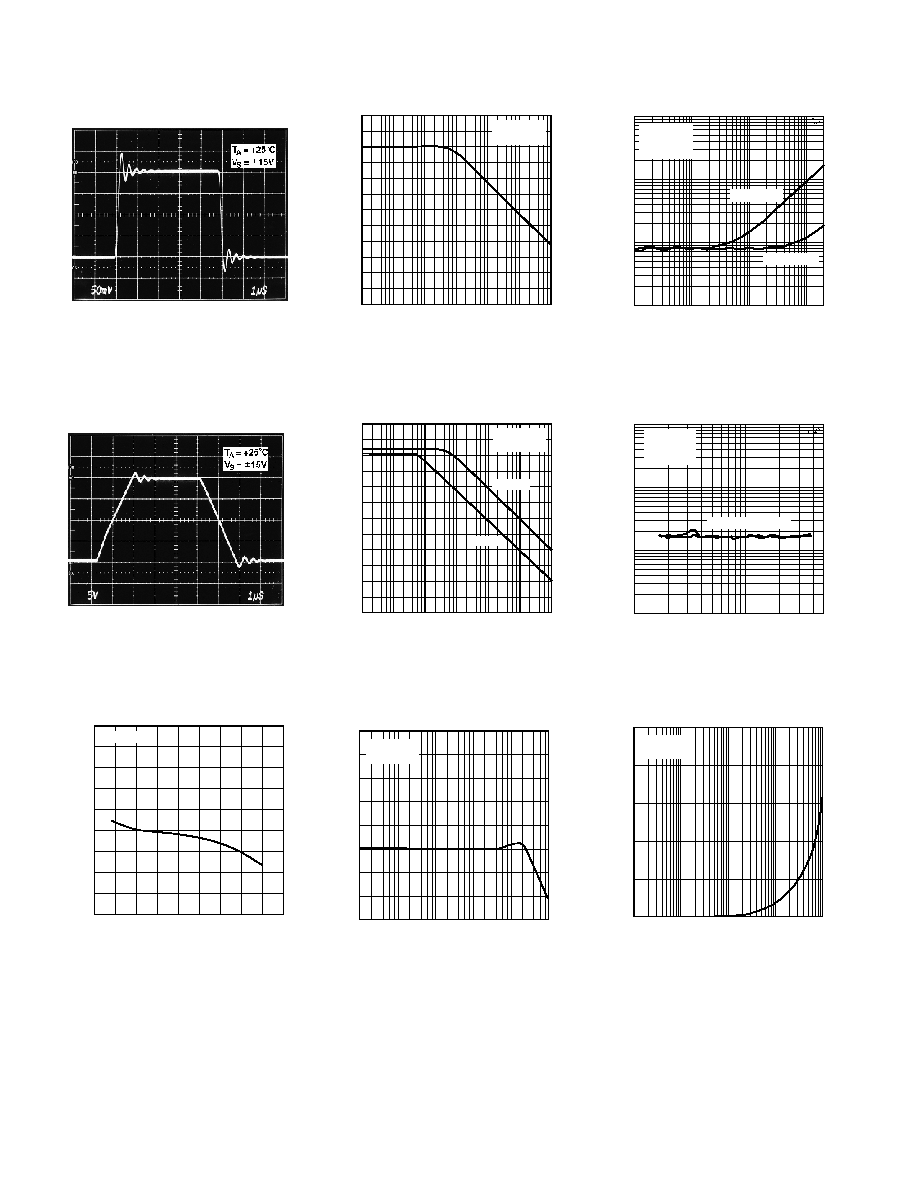
Figure 1. Small Signal Transient
Response
Figure 4. Large Signal Transient
Response
INPUT OFFSET VOLTAGE ≠
V
1000
800
≠800
0
≠200
≠400
≠600
600
200
400
TEMPERATURE ≠ C
≠75 ≠50
150
≠25
0
25
75
100 125
50
V
S
= 15V
Figure 7. Input Offset Voltage vs.
Temperature
FREQUENCY ≠ Hz
COMMON-MODE REJECTION ≠ dB
120
0
1
10
1M
100
1k
10k
100k
90
40
30
20
10
80
70
50
60
110
100
T
A
= +25 C
V
S
= 15V
Figure 2. Common-Mode Rejection
vs. Frequency
FREQUENCY ≠ Hz
POWER SUPPLY REJECTION ≠ dB
120
0
1
10
1M
100
1k
10k
100k
90
40
30
20
10
80
70
50
60
110
100
T
A
= +25 C
V
S
= 15V
≠PSRR
+PSRR
Figure 5. Power Supply Rejection
vs. Frequency
FREQUENCY ≠ Hz
CLOSED-LOOP GAIN ≠ dB
50
40
≠30
100
1k
10M
10k
100k
1M
10
0
≠10
≠20
30
20
T
A
= +25∞C
V
S
= 15V
Figure 8. Closed-Loop Gain vs.
Frequency
FREQUENCY ≠ Hz
THD+N ≠ %
0.1
0.010
0.0001
20
100
20k
0.001
1k
10k
T
A
= +25 C
V
S
= 15V
A
V
= ≠1
R
L
= 600
R
L
= 100k
Figure 3. Total Harmonic Distortion
vs. Frequency
FREQUENCY ≠ Hz
0.1
0.010
0.0001
2k
50k
0.001
10k
DIM ≠ %
T
A
= +25 C
V
S
= 15V
A
V
= ≠1
R
L
= 600 , 100k
Figure 6. Dynamic Intermodulation
Distortion vs. Frequency
FREQUENCY ≠ Hz
OUTPUT IMPEDANCE ≠
10
8
0
100
1k
1M
10k
100k
6
4
2
T
A
= +25∞C
V
S
= 15V
Figure 9. Closed-Loop Output Imped-
ance vs. Frequency

AMP03
≠5≠
REV. E
TEMPERATURE ≠ C
GAIN ERROR ≠ %
0.003
≠75 ≠50
100
≠25
0
25
50
75
0.002
0.000
≠0.001
≠0.002
≠0.003
0.001
125 150
V
S
= 15V
R
S
= 0
Figure 10. Gain Error vs. Temperature
SUPPLY VOLTAGE ≠ Volts
SUPPLY CURRENT ≠ mA
4
0
0
5
20
10
15
2
1
3
T
A
= +25 C
Figure 13. Supply Current vs. Supply
Voltage
FREQUENCY ≠ Hz
120
100
0
1
10
10k
100
1k
80
60
40
20
T
A
= +25 C
V
S
= 15V
Hz
VOLTAGE NOISE DENSITY ≠ nV/
Figure 16. Voltage Noise Density vs.
Frequency
+10 V
0V
≠10 V
NOTE: EXTERNAL AMPLIFIER GAIN = 1000;
THEREFORE, VERTICAL SCALE = 10 V/DIV.
Figure 19. Voltage Noise from 0 kHz to 10 kHz
TEMPERATURE ≠ C
SLEW RATE ≠ V/
s
13
6
≠75 ≠50
125
≠25
0
25
50
75
100
12
10
9
8
7
11
V
S
= 15V
R
L
= 2k
Figure 11. Slew Rate vs. Temperature
OUTPUT SOURCE CURRENT ≠ mA
17.5
0
0
6
36
12
18
24
30
15.0
12.5
10.0
5.0
2.5
7.5
MAXIMUM OUTPUT VOLTAGE ≠ Volts
T
A
= +25 C
V
S
= 18V
V
S
= 15V
V
S
= 12V
V
S
= 9V
V
S
= 5V
Figure 14. Maximum Output Voltage
vs. Output Current (Source)
+1 V
0V
≠1 V
0.1 TO 10Hz PEAK-TO-PEAK NOISE
Figure 17. Low Frequency Voltage
Noise
TEMPERATURE ≠ C
SUPPLY CURRENT ≠ mA
6
≠75 ≠50
125
≠25
0
25
50
75 100
5
3
2
1
0
4
150
V
S
= 15V
Figure 12. Supply Current vs.
Temperature
OUTPUT SINK CURRENT ≠ mA
≠17.5
0
0
≠2
≠12
≠4
≠6
≠8
≠10
≠15.0
≠12.5
≠10.0
≠5.0
≠2.5
≠7.5
MAXIMUM OUTPUT VOLTAGE ≠ Volts
T
A
= +25 C
V
S
= 18V
V
S
= 15V
V
S
= 12V
V
S
= 9V
V
S
= 5V
Figure 15. Maximum Output Voltage
vs. Output Current (Sink)
+10 V
0V
≠10 V
NOTE: EXTERNAL AMPLIFIER GAIN = 1000;
THEREFORE, VERTICAL SCALE = 10 V/DIV.
Figure 18. Voltage Noise from 0 kHz
to 1 kHz
AMP03
≠6≠
REV. E
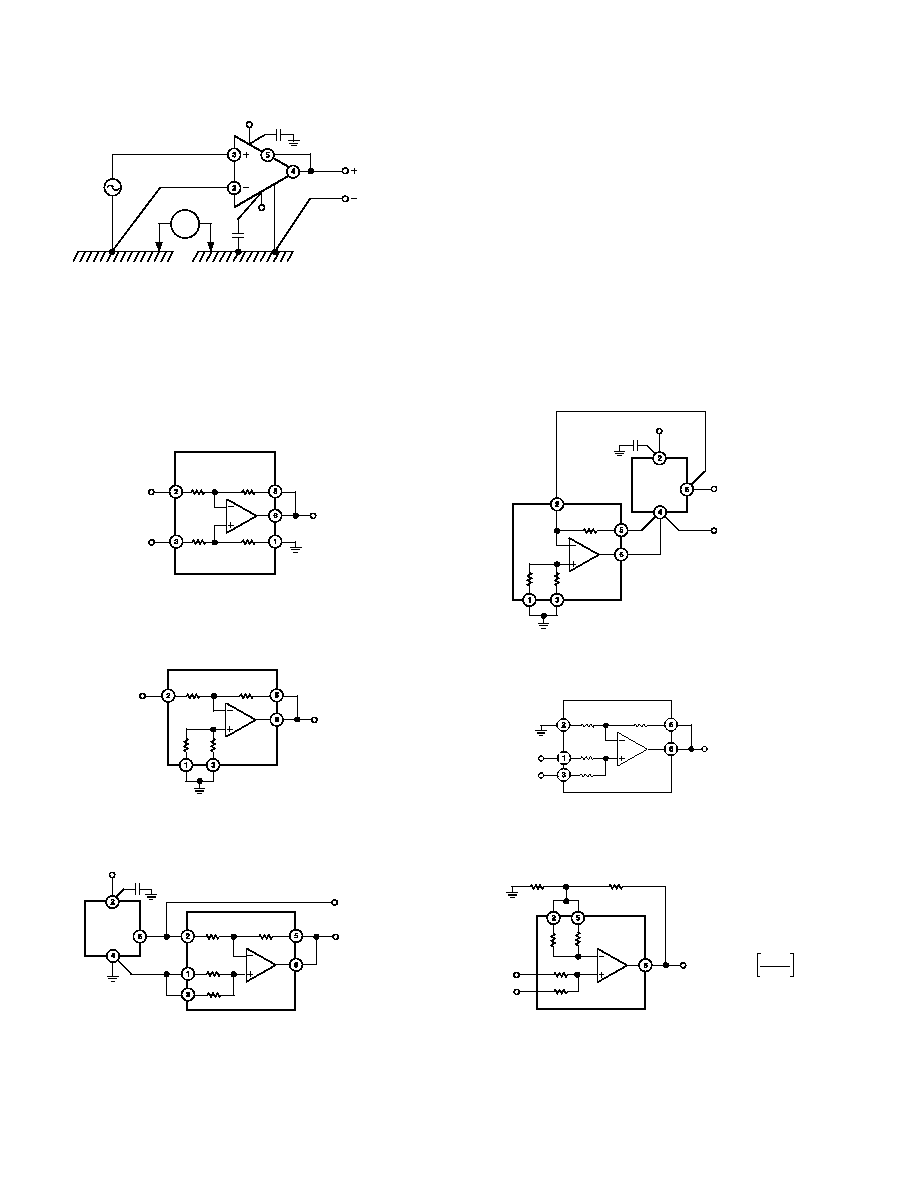
ECM
+V
0.1 F
0.1 F
≠V
V
SIGNAL
GROUND REFERENCE 1
GROUND REFERENCE 2
(GROUND REFERENCE 2)
V
OUT
= ≠V
SIGNAL
AMP03
Figure 20. AMP03 Serves to Reject Common-Mode Volt-
ages in Instrumentation Systems. Common-Mode Volt-
ages Occur Due to Ground Current Returns. V
SIGNAL
and
E
CM
Must Be Within the Common-Mode Range of AMP03.
APPLICATIONS INFORMATION
The AMP03 represents a versatile analog building block. In
order to capitalize on fast settling time, high slew rate and high
CMR, proper decoupling and grounding techniques must be
employed. Figure 20 illustrates the use of 0.1
µ
F decoupling
capacitors and proper ground connections.
MAINTAINING COMMON-MODE REJECTION
In order to achieve the full common-mode rejection capability
of the AMP03, the source impedance must be carefully con-
trolled. Slight imbalances of the source resistance will result in a
degradation of DC CMR--even a 5
imbalance will degrade
CMR by 20 dB. Also, the matching of the reactive source im-
pedance must be matched in order to preserve the CMRR over
frequency.
APPLICATION CIRCUITS
AMP03
R
1
25k
R
2
25k
R
3
25k
R
4
25k
+IN E
2
≠IN E
1
E
0
= E
2
≠E
1
Figure 21. Precision Difference Amplifier. Rejects
Common-Mode Signal = (E
1
+ E
2
)/2 by 100 dB
AMP03
E
1
E
0
= ≠E
1
Figure 22. Precision Unity-Gain Inverting Amplifier
AMP03
+15V
≠10V OUT
0.1 F
REF10
+10V OUT
Figure 23.
10 V Precision Voltage Reference
+15V
≠5V OUT
0.1 F
REF10
+5V OUT
AMP03
Figure 24.
5 V Precision Voltage Reference
AMP03
E
1
E
2
E
0
= E
1
+ E
2
Figure 25. Precision Summing Amplifier
AMP03
R
2
R
1
E
1
E
2
E
0
= (R
2
/R
1
+1)
E
1
= E
2
2
Figure 26. Precision Summing Amplifier with Gain

AMP03
≠7≠
REV. E
System Design
Suggested Op Amp
Requirement
For A1 and A2
Source Impedance Low, Need Low
OP27, OP37
Voltage Noise Performance
OP227 (Dual Matched)
OP270 (Dual)
OP271
OP470
OP471
Source Impedance High
OP80
(R
S
15 k
). Need Low Current
OP41
Noise
OP43
OP249
OP97
Require Ultrahigh Input Impedance
OP80
OP97
OP41
OP43
Need Wider Bandwidth and High
OP42
Speed
OP43
OP249
AMP03
OP80EJ
LOAD
I
0
I
0
= (E
1
≠ E
2
)/R
E
1
E
2
R
Figure 27. Differential Input Voltage-to-Current Converter
for Low I
OUT
. OP80EJ Maintains 250 fA Max Input Current,
Allowing I
O
to Be Less Than 1 pA
AMP03
R
2
R
2
R
1
≠IN E
1
+IN E
2
A
1
A
2
E
0
OUTPUT
E
0
= (1 + 2R
2
/R
1
) (E
2
≠ E
1
)
Figure 28. Suitable Instrumentation Amplifier Requirements
Can Be Addressed by Using an Input Stage Consisting of A
1
,
A
2
, R
1
and R
2
. The Following Matrix Suggests a Suitable
Amplifier.
AMP03
≠8≠
REV. E
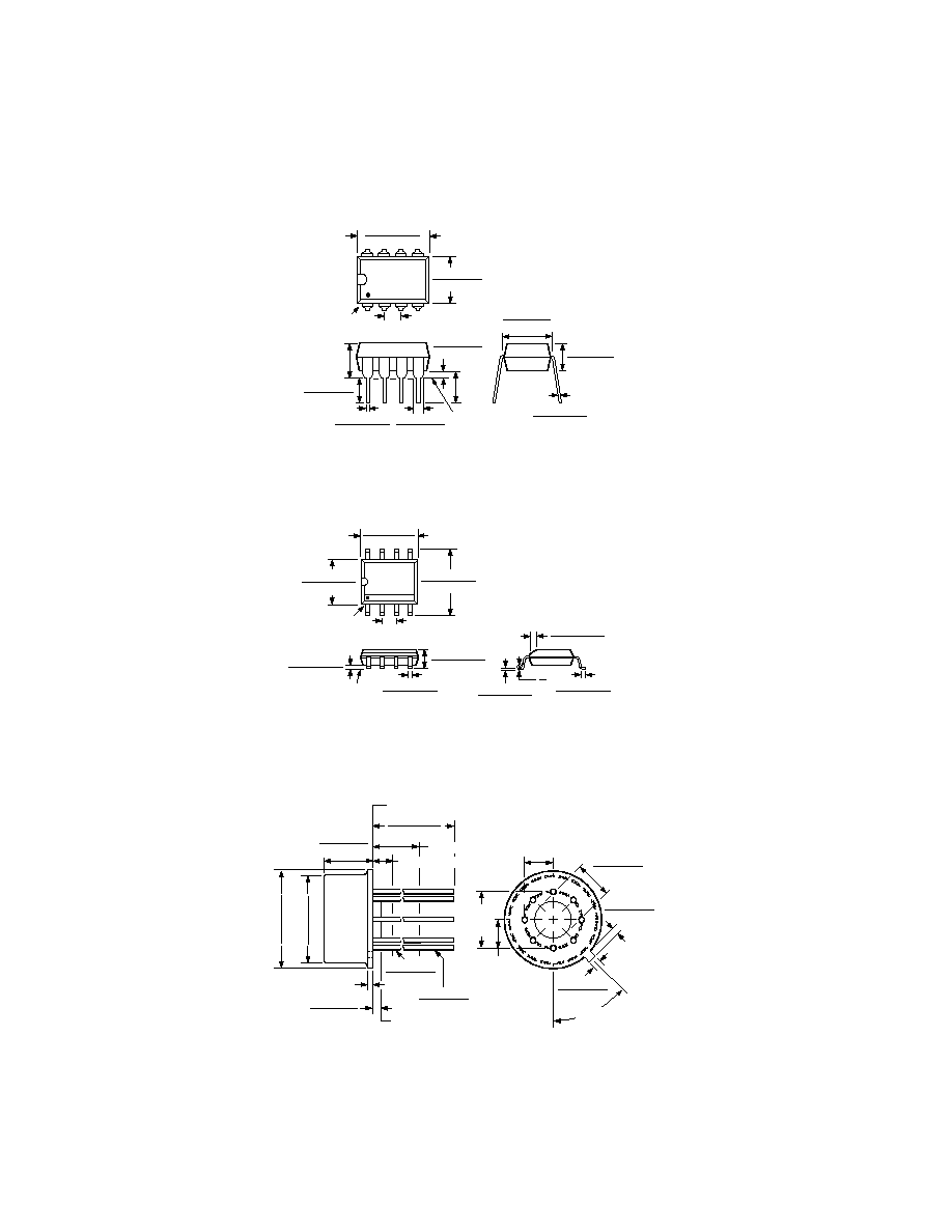
OUTLINE DIMENSIONS
Dimensions shown in inches and (mm).
C3154e≠0≠8/99
PRINTED IN U.S.A.
8-Lead Plastic DIP
(N-8)
SEATING
PLANE
0.060 (1.52)
0.015 (0.38)
0.210
(5.33)
MAX
0.022 (0.558)
0.014 (0.356)
0.160 (4.06)
0.115 (2.93)
0.070 (1.77)
0.045 (1.15)
0.130
(3.30)
MIN
8
1
4
5
PIN 1
0.280 (7.11)
0.240 (6.10)
0.100 (2.54)
BSC
0.430 (10.92)
0.348 (8.84)
0.195 (4.95)
0.115 (2.93)
0.015 (0.381)
0.008 (0.204)
0.325 (8.25)
0.300 (7.62)
8-Lead SOIC
(SO-8)
8
5
4
1
0.1968 (5.00)
0.1890 (4.80)
0.2440 (6.20)
0.2284 (5.80)
PIN 1
0.1574 (4.00)
0.1497 (3.80)
0.0500 (1.27)
BSC
0.0688 (1.75)
0.0532 (1.35)
SEATING
PLANE
0.0098 (0.25)
0.0040 (0.10)
0.0192 (0.49)
0.0138 (0.35)
0.0098 (0.25)
0.0075 (0.19)
0.0500 (1.27)
0.0160 (0.41)
8
0
0.0196 (0.50)
0.0099 (0.25)
45
8-Lead Metal Can
(H-08B)
0.250 (6.35) MIN
0.750 (19.05)
0.500 (12.70)
0.185 (4.70)
0.165 (4.19)
REFERENCE PLANE
0.050 (1.27) MAX
0.019 (0.48)
0.016 (0.41)
0.021 (0.53)
0.016 (0.41)
0.045 (1.14)
0.010 (0.25)
0.040 (1.02) MAX
BASE & SEATING PLANE
0.335 (8.51)
0.305 (7.75)
0.370 (9.40)
0.335 (8.51)
0.034 (0.86)
0.027 (0.69)
0.045 (1.14)
0.027 (0.69)
0.160 (4.06)
0.110 (2.79)
0.100 (2.54) BSC
6
2
8
7
5
4
3
1
0.200
(5.08)
BSC
0.100
(2.54)
BSC
45∞ BSC