REV. A
Information furnished by Analog Devices is believed to be accurate and
reliable. However, no responsibility is assumed by Analog Devices for its
use, nor for any infringements of patents or other rights of third parties
which may result from its use. No license is granted by implication or
otherwise under any patent or patent rights of Analog Devices.
a
28 V/100 W DC/DC Converters
with Integral EMI Filter
ADDC02812DA/ADDC02815DA
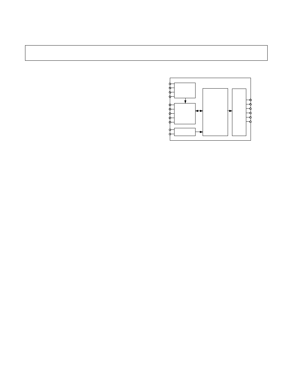
FUNCTIONAL BLOCK DIAGRAM
OUTPUT
FILTER
V
COM
V
COM
+SENSE
ADJUST
STATUS
V
AUX
INHIBIT
SYNC
I
SHARE
TEMP
≠V
IN
+V
IN
FIXED
FREQUENCY
DUAL
INTERLEAVED
POWER TRAIN
≠SENSE
≠V
OUT
≠V
OUT
+V
OUT
+V
OUT
INPUT SIDE
CONTROL
CIRCUIT
EMI FILTER
OUTPUT SIDE
CONTROL
CIRCUIT
ADDC02812DA/ADDC02815DA
FEATURES
28 V dc Input, 12 V dc @ 8.34 A, 100 W Output
(ADDC02812DA)
28 V dc Input, 15 V dc @ 6.68 A, 100 W Output
(ADDC02815DA)
Integral EMI Filter Designed to Meet MIL-STD-461D
Low Weight: 80 Grams
NAVMAT Derated
Many Protection and System Features
APPLICATIONS
Commercial and Military Airborne Electronics
Missile Electronics
Space-Based Antennae and Vehicles
Mobile/Portable Ground Equipment
GENERAL DESCRIPTION
The ADDC02812DA and ADDC02815DA hybrid military dc/
dc converters with integral EMI filter offer the highest power
density of any dc/dc power converters with their features and in
their power range available today. The converters with integral
EMI filter are a fixed frequency, 1 MHz, square wave switching
dc/dc power supply. They are not variable frequency resonant
converters. In addition to many protection features, these con-
verters have system level features that allow them to be used as a
component in larger systems as well as a stand-alone power
supply. The units are designed for high reliability and high
performance applications where saving space and/or weight are
critical.
The ADDC02812DA and ADDC02815DA are available in a
hermetically sealed, molybdenum based hybrid package and are
easily heatsink mountable. Three screening levels are available,
including military SMD.
PRODUCT HIGHLIGHTS
1. 60 W/cubic inch power density with an integral EMI filter
designed to meet all applicable requirements in MIL-STD-
461D when installed in a typical system setup
2. Light weight: 80 grams
3. Operational and survivable over a wide range of input
conditions: 16 V≠50 V dc; survives low line, high line, and
positive and negative transients
4. High reliability; NAVMAT derated
5. Protection features include:
Output Overvoltage Protection
Output Short Circuit Current Protection
Thermal Monitor/Shutdown
Input Overvoltage Shutdown
Input Transient Protection
6. System level features include:
Current Sharing for Parallel Operation
Inhibit Control
Output Status Signal
Synchronization for Multiple Units
Input Referenced Auxiliary Voltage
One Technology Way, P.O. Box 9106, Norwood, MA 02062-9106, U.S.A.
Tel: 781/329-4700
World Wide Web Site: http://www.analog.com
Fax: 781/326-8703
© Analog Devices, Inc., 1997

Case
Test
ADDC02812DA
ADDC02815DA
Parameter
Temp
Level Conditions
Min
Typ
Max
Min
Typ
Max
Units
INPUT CHARACTERISTICS
Steady State Operating Input
Voltage Range
1
(12 V)
Full
VI
I
O
=
±
0.42 A to
±
4.17 A
18
28
40
V dc
Steady State Operating Input
Voltage Range
1
(15 V)
Full
VI
I
O
=
±
0.34 A to
±
3.34 A
18
28
40
V dc
Abnormal Operating Input Voltage
Range (per MIL-STD-704D)
1
(12 V)
Full
VI
I
O
=
±
0.42 A to
±
3.34 A
16
50
V dc
Abnormal Operating Input Voltage
Range (per MIL-STD-704D)
1
(15 V)
Full
VI
I
O
=
±
0.34 A to
±
2.67 A
16
50
V dc
Input Voltage Shutdown (12 V/15 V)
+25
∞
C
I
50
52
55
50
52
55
V dc
No Load Input Current (12 V/15 V)
+25
∞
C
I
85
100
85
100
mA
Disabled Input Current (12 V/15 V)
Full
VI
1
2
1
2
mA
OUTPUT CHARACTERISTICS
2, 3, 4
Regulated Output Voltage (+12 V)
+25
∞
C
I
I
O
=
±
0.42 A to
±
4.17 A,
+11.88 +12.00 +12.12
V dc
V
IN
= 18 to 40 V dc
Full
VI
I
O
=
±
0.42 A to
±
4.17 A,
+11.76
+12.24
V dc
V
IN
= 18 to 40 V dc
Full
VI
I
O
=
±
0.42 A to
±
4.17 A,
+11.76
+12.24
V dc
V
IN
= 16 to 50 V dc
Regulated Output Voltage (+15 V)
+25
∞
C
I
I
O
=
±
0.34 A to
±
3.34 A,
+14.85 +15.00 +15.15
V dc
V
IN
= 18 to 40 V dc
Full
VI
I
O
=
±
0.34 A to
±
3.34 A,
+14.70
+15.30
V dc
V
IN
= 18 to 40 V dc
Full
VI
I
O
=
±
0.34 A to
±
3.34 A,
+14.70
+15.30
V dc
V
IN
= 16 to 50 V dc
Cross Regulated Output Voltage (≠12 V)
+25
∞
C
I
I
O
=
±
0.42 A to
±
4.17 A,
≠12.24 ≠12.00 ≠11.76
V dc
V
IN
= 18 to 40 V dc
Full
VI
I
O
=
±
0.42 A to
±
4.17 A,
≠12.36
≠11.64
V dc
V
IN
= 18 to 40 V dc
Full
VI
I
O
=
±
0.42 A to
±
4.17 A,
≠12.36
≠11.64
V dc
V
IN
= 16 to 50 V dc
Cross Regulated Output Voltage (≠15 V)
+25
∞
C
I
I
O
=
±
0.34 A to
±
3.34 A,
≠14.70 ≠15.00 ≠15.30
V dc
V
IN
= 18 to 40 V dc
Full
VI
I
O
=
±
0.34 A to
±
3.34 A,
≠14.55
≠15.45
V dc
V
IN
= 18 to 40 V dc
Full
VI
I
O
=
±
0.34 A to
±
3.34 A,
≠14.55
≠15.45
V dc
V
IN
= 16 to 50 V dc
Line Regulation (12 V)
+25
∞
C
V
I
O
=
±
4.17 A,
4
mV
V
IN
= 18 to 40 V dc
Line Regulation (15 V)
+25
∞
C
V
I
O
=
±
3.34 A,
5
mV
V
IN
= 18 to 40 V dc
Load Regulation (12 V)
+25
∞
C
V
V
IN
= 28 V dc,
4
mV
I
O
=
±
0.42 A to +4.17 A
Load Regulation (15 V)
+25
∞
C
V
V
IN
= 28 V dc,
6
mV
I
O
=
±
0.34 A to +3.34 A
Output Ripple/Noise (Regulated +12 V)
5
+25
∞
C
I
I
O
=
±
4.17 A,
45
mV p-p
(Cross Regulated ≠12 V)
5
5 kHz ≠ 2 MHz BW
55
mV p-p
Output Ripple/Noise (Regulated +15 V)
5
+25
∞
C
I
I
O
=
±
3.34 A,
45
mV p-p
(Cross Regulated ≠15 V)
5
5 kHz ≠ 2 MHz BW
50
mV p-p
Total Output Current (I
O
) 12 V
Full
VI
V
O
=
±
12 V dc,
0.833
8.34
A
V
IN
= 18 to 40 V dc
Total Output Current (I
O
) 15 V
Full
VI
V
O
=
±
15 V dc,
0.68
6.68
A
V
IN
= 18 to 40 V dc
Output Overvoltage Protection (12 V)
+25
∞
C
V
I
O
=
±
4.17 A, Open
118
% V nom
Remote Sense Connection
Output Overvoltage Protection (15 V)
+25
∞
C
V
I
O
=
±
3.34 A, Open
118
% V nom
Remote Sense Connection
Output Current Limit (12 V/15 V)
+25
∞
C
V
V
O
= 90% V
OUT
Nom
130
130
% I
O
max
Output Short Circuit Current (12 V/15 V)
+25
∞
C
I
15.5
14.5
A
ISOLATION CHARACTERISTICS
Isolation Voltage
+25
∞
C
I
Input to Output or Any Pin
100
100
M
to Case at 500 V dc
REV. A
≠2≠
(T
C
= 25 C, V
IN
= 28 V dc unless otherwise noted; full temperature range is ≠55 C to
+90 C; all temperatures are case and T
C
is the temperature measured at the center of the package bottom.)
ADDC02812DA/ADDC02815DA≠SPECIFICATIONS
ELECTRICAL CHARACTERISTICS

Case
Test
ADDC02812DA
ADDC02815DA
Parameter
Temp
Level Conditions
Min
Typ
Max
Min
Typ
Max
Units
DYNAMIC CHARACTERISTICS
6
Output Voltage Deviation Due to Step
+25
∞
C
V
I
O
=
±
2.08 A to
±
4.17 A
0.850
V
Change in Load (12 V)
or
±
4.17 A to
±
2.08 A
Output Voltage Deviation Due to Step
+25
∞
C
V
I
O
=
±
1.67 A to
±
3.34 A
0.850
V
Change in Load (15 V)
or
±
3.34 A to
±
1.67 A
Response Time Due to Step
+25
∞
C
V
I
O
=
±
2.08 A to
±
4.17 A
150
µ
s
Change in Load (12 V)
or
±
4.17 A to
±
2.08 A
di/dt = 0.5 A/
µ
s, Measured
to Within 2% of Final Value
Response Time Due to Step Change
+25
∞
C
V
I
O
=
±
1.67 A to
±
3.34 A or
150
µ
s
in Load (15 V)
±
3.34 A to
±
1.67 A,
di/dt = 0.5 A/
µ
s, Measured
to Within 2% of Final Value
Soft Start Turn-On Time (12 V)
+25
∞
C
I
I
O
=
±
4.17 A, from Inhibit
6
15
ms
High to Status High
Soft Start Turn-On Time (15 V)
+25
∞
C
I
I
O
=
±
3.34 A, from Inhibit
6
15
ms
High to Status High
THERMAL CHARACTERISTICS
Efficiency (12 V)
+25
∞
C
I
I
O
=
±
2.5 A
81
85
%
+90
∞
C
VI
I
O
=
±
2.5 A
81
%
≠55
∞
C
VI
I
O
=
±
2.5 A
80
%
+25
∞
C
I
I
O
=
±
4.17 A
81
85
%
+90
∞
C
VI
I
O
=
±
4.17 A
81
%
≠55
∞
C
VI
I
O
=
±
4.17 A
80
%
Efficiency (15 V)
+25
∞
C
I
I
O
=
±
2.0 A
81
85
%
+90
∞
C
VI
I
O
=
±
2.0 A
81
%
≠55
∞
C
VI
I
O
=
±
2.0 A
80
%
+25
∞
C
I
I
O
=
±
3.34 A
81
85
%
+90
∞
C
VI
I
O
=
±
3.34 A
81
%
≠55
∞
C
VI
I
O
=
±
3.34 A
80
%
Hottest Junction Temperature
7
(12 V)
+90
∞
C
V
I
O
=
±
4.17 A
110
∞
C
Hottest Junction Temperature
7
(15 V)
+90
∞
C
V
I
O
=
±
3.34 A
110
∞
C
CONTROL CHARACTERISTICS
Clock Frequency (12 V)
Full
VI
I
O
=
±
0.42 A
0.85
0.99
MHz
Clock Frequency (15 V)
Full
VI
I
O
=
±
0.34 A
0.85
0.99
MHz
Adjust (Pin 3) V
ADJ
(12 V)
+25
∞
C
I
4.7
4.8
4.9
V
Adjust (Pin 3) V
ADJ
(15 V)
+25
∞
C
I
5.9
6.0
6.1
V
Status (Pin 4)
V
OH
+25
∞
C
I
I
OH
= 400
µ
A
2.4
4.0
2.4
4.0
V
V
OL
+25
∞
C
I
I
OL
= 1 mA
0.15
0.7
0.15
0.7
V
V
AUX
(Pin 5)
V
O
(nom) (12 V)
+25
∞
C
I
I
AUX
= 5 mA, Load
13.00
13.5
14.00
V
Current =
±
4.17 A
V
AUX
(Pin 5)
V
O
(nom) (15 V)
+25
∞
C
I
I
AUX
= 5 mA, Load
13.5
13.9
14.5
V
Current =
±
3.34 A
Inhibit (Pin 6)
V
IL
+25
∞
C
I
0.5
0.5
V
I
IL
+25
∞
C
I
V
IL
= 0.5 V
1.2
1.2
mA
V
I
(Open Circuit)
+25
∞
C
I
15
15
V
SYNC (Pin 7)
8
V
IH
+25
∞
C
I
4.0
4.0
V
I
IH
+25
∞
C
I
V
IH
= 7.0 V
175
175
µ
A
I
SHARE
(Pin 8) (12 V)
+25
∞
C
I
Load Current =
±
4.17 A
2.65
2.75
2.85
V
I
SHARE
(Pin 8) (15 V)
+25
∞
C
I
Load Current =
±
3.34 A
2.65
2.75
2.85
V
Temp (Pin 9)
+25
∞
C
V
3.90
3.90
V
NOTES
1
Military subgroups apply only to military qualified devices.
2
50 V dc upper limit rated for transient condition of up to 50 ms. 16 V dc lower limit rated for continuous operation during emergency condition. Steady state and abnormal
input voltage range require source impedance sufficient to insure input stability at low line. See sections entitled System Instability Considerations and Input Voltage Range.
3
Measured at the remote sense points.
4
Output characteristics tested with balanced loads on each output; however, unit operates with unbalanced loads up to 90%/10% split.
5
Regulated output typically performs with less ripple than cross regulated output. 100% test is performed with VD+ regulated and VD≠ cross regulated.
6
C
LOAD
= 0.
7
Refer to section entitled Thermal Characteristics for more information.
8
Unit has internal pull-down; refer to section entitled Pin 7 (SYNC).
Specifications subject to change without notice.
REV. A
≠3≠
ADDC02812DA/ADDC02815DA

≠4≠
ADDC02812DA/ADDC02815DA
REV. A
ABSOLUTE MAXIMUM RATINGS*
INHIBIT . . . . . . . . . . . . . . . . . . . . . . . . . . 50 V dc, ≠0.5 V dc
SYNC . . . . . . . . . . . . . . . . . . . . . . . . . . . . . 8 V dc, ≠0.5 V dc
I
SHARE
. . . . . . . . . . . . . . . . . . . . . . . . . . . . . 6 V dc, ≠0.5 V dc
TEMP . . . . . . . . . . . . . . . . . . . . . . . . . . . . 12 V dc, ≠0.3 V dc
Lead Soldering Temp (10 sec) . . . . . . . . . . . . . . . . . . . +300
∞
C
Storage Temperature . . . . . . . . . . . . . . . . . . ≠65
∞
C to +150
∞
C
Maximum Junction Temperature . . . . . . . . . . . . . . . . +150
∞
C
Maximum Case Operating Temperature . . . . . . . . . . . +125
∞
C
*Absolute maximum ratings are limiting values, to be applied individually, and
beyond which the serviceability of the circuit may be impaired. Functional
operability under any of these conditions is not necessarily implied. Exposure of
absolute maximum rating conditions for extended periods of time may affect
device reliability.
ORDERING GUIDE
Operating
Temperature
Package
Model
Range (Case)
Description
ADDC02812DAKV
≠40
∞
C to +85
∞
C
Hermetic
ADDC02812DATV
≠55
∞
C to +90
∞
C
Hermetic
5962-9684101HXC
(ADDC02812DATV/QMLH) ≠55
∞
C to +125
∞
C
Hermetic
ADDC02815DAKV
≠40
∞
C to +85
∞
C
Hermetic
ADDC02815DATV
≠55
∞
C to +90
∞
C
Hermetic
5962-9684201HXC
(ADDC02815DATV/QMLH) ≠55
∞
C to +125
∞
C
Hermetic
EXPLANATION OF TEST LEVELS
Test Level
I
≠ 100% production tested.
II
≠ 100% production tested at +25
∞
C, and sample tested
at specified temperatures.
III ≠ Sample tested only.
IV ≠ Parameter is guaranteed by design and characterization
testing.
V
≠ Parameter is a typical value only.
VI ≠ All devices are 100% production tested at +25
∞
C. 100%
production tested at temperature extremes for military
temperature devices; guaranteed by design and charac-
terization testing for industrial devices.
PIN CONFIGURATION
1
11
12
17
TOP
VIEW
PIN DESCRIPTIONS
Pin
No.
Name
Function
1
≠SENSE
Feedback loop connection for remote sensing
output voltage. Must always be connected for
proper operation.
2
+SENSE
Feedback loop connection for remote sensing
output voltage. Must always be connected
for proper operation.
3
ADJUST
Adjusts output voltage setpoint.
4
STATUS
Indicates output voltage is within
±
5% of
nominal. Active high referenced to ≠SENSE
(Pin 1).
5
V
AUX
Low level dc auxiliary voltage supply refer-
enced to input return (Pin 10).
6
INHIBIT
Power supply disable. Active low and refer-
enced to input return (Pin 10).
7
SYNC
Clock synchronization input for multiple
units; referenced to input return (Pin 10).
8
I
SHARE
Current share pin which allows paralleled
units to share current typically within
±
5% at
full load; referenced to input return (Pin 10).
9
TEMP
Case temperature indicator and temperature
shutdown override; referenced to input return
(Pin 10).
10
≠V
IN
Input Return.
11
+V
IN
+28 V Nominal Input Bus.
12
+V
OUT
+12 V dc Output (ADDC02812DA).
+15 V dc Output (ADDC02815DA).
13
+V
OUT
+12 V dc Output (ADDC02812DA).
+15 V dc Output (ADDC02815DA).
14
V
COMMON
Output Return.
15
V
COMMON
Output Return.
16
≠V
OUT
≠12 V dc Output (ADDC02812DA).
≠15 V dc Output (ADDC02815DA).
17
≠V
OUT
≠12 V dc Output (ADDC02812DA).
≠15 V dc Output (ADDC02815DA).
CAUTION
ESD (electrostatic discharge) sensitive device. Electrostatic charges as high as 4000 V readily
accumulate on the human body and test equipment and can discharge without detection. Although
the ADDC02812DA/ADDC02815DA feature proprietary ESD protection circuitry, permanent
damage may occur on devices subjected to high energy electrostatic discharges. Therefore, proper
ESD precautions are recommended to avoid performance degradation or loss of functionality.
WARNING!
ESD SENSITIVE DEVICE
ADDC02812DA/ADDC02815DA
REV. A
≠5≠
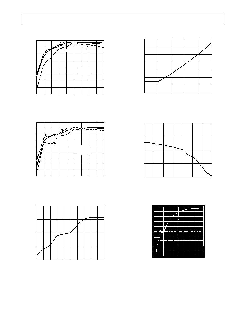
Typical Performance Curves
OUTPUT POWER ≠ Watts
86
70
10
100
20
30
40
50
60
70
80
90
84
78
76
74
72
82
80
40V
18V
28V
EFFICIENCY ≠ %
V
IN
= 28V
V
O
= +12V
T
C
= +25 C
Figure 1. Efficiency vs. Line and Load at +25
∞
C
(ADDC02812DA)
OUTPUT POWER ≠ Watts
10
100
20
30
40
50
60
70
80
90
88
86
70
78
76
74
72
82
80
84
28V
18V
40V
EFFICIENCY ≠ %
V
IN
= 28V
V
O
= 15V
T
C
= +25 C
Figure 2. Efficiency vs. Line and Load at +25
∞
C
(ADDC02815DA)
T
CASE
≠ C
87
EFFICIENCY ≠ %
86
83
≠55
90
≠45
≠35
≠15
≠5
5
25
45
65
85
85
84
Figure 3. Efficiency vs. Case Temperature (
∞
C)
(at Nominal V
IN
, 75% Max Load, ADDC02812DA)
OUTPUT POWER ≠ Watts
INPUT VOLTAGE
14.4
14.2
13.0
50
100
60
70
80
90
13.8
13.6
13.4
13.2
14.0
Figure 4. Low Line Dropout vs. Load at 90
∞
C Case
Temperature
T
CASE
≠ C
V
OUT
DEVIATION ≠ %
1.00
0.50
≠1.00
≠55
90
≠35
≠15
5
25
55
75
0.00
≠0.50
Figure 5. Normalized Output Voltage vs. Case
Temperature (
∞
C)
V
INHIBIT
V
O
2V
/DIV
1ms
Figure 6. Output Voltage Transient During Turn-On
with Minimum Load Displaying Soft Start When Supply
Is Enabled
≠6≠
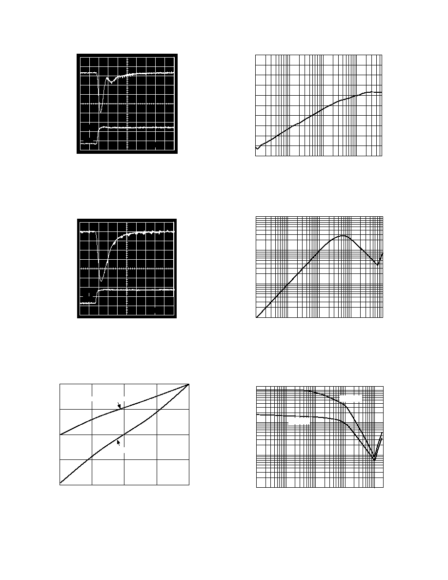
ADDC02812DA/ADDC02815DA
REV. A
V
O
I
O
100W
50W
200mV
/DIV
50 s
Figure 7. Output Voltage Transient Response to a 50% to
a 100% Step Change in Load with Zero Load Capacitance
(ADDC02812DA)
50 s
I
O
V
O
200mV
/DIV
100W
50W
Figure 8. Output Voltage Transient Response to a 50% to
a 100% Step Change in Load with Zero Load Capacitance
(ADDC02815DA)
% FULL POWER REGULATED OUTPUT
4
2
CROSS REGULATION ≠ %
≠4
10
90
30
50
70
0
≠2
UNREGULATED OUTPUT @ 10%
FULL POWER
Figure 9. Cross Regulation Envelope
FREQUENCY ≠ Hz
0
AS
≠ dB
≠30
≠100
10
50k
100
1k
10k
≠50
≠80
≠10
≠20
≠40
≠60
≠70
≠90
Figure 10. Audio Susceptibility (Magnitude of V
OUT
/V
IN
)
Z
OUT
≠ m
FREQUENCY ≠ kHz
1000
100
1
0.01
100
0.1
1
10
10
Figure 11. Incremental Output Impedance (Magnitude)
Z
IN
≠
FREQUENCY ≠ kHz
10
1
≠0.01
0.01
100
0.1
1
10
≠0.1
V
IN
= 28V
V
IN
= 18V
Figure 12. Incremental Input Impedance (Magnitude)
ADDC02812DA/ADDC02815DA
REV. A
≠7≠
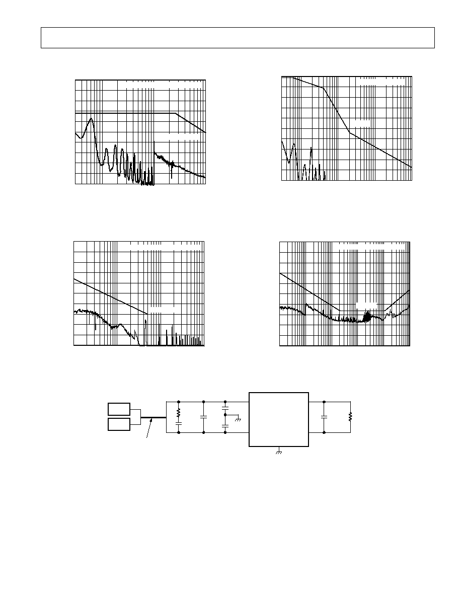
Typical EMI Curves and Test Setup
FREQUENCY ≠ MHz
130
0.01
0.0001
0.001
70
90
30
EMISSION LEVEL ≠ dB
V
110
50
CONDUCTED EMISSIONS CE≠101
CE101≠1 4.5 AMPS
Figure 13. Conducted Emissions, MIL-STD-461D, CE101,
+28 V Hot Line 100 W Load
FREQUENCY ≠ MHz
130
10
0.01
0.1
70
90
30
EMISSION LEVEL ≠ dB
V
110
50
1
CONDUCTED EMISSIONS CE≠102
LIMIT 28VDC
Figure 14. Conducted Emissions, MIL-STD-461D, CE102,
+28 V Hot Line 100 W Load
FREQUENCY ≠ MHz
166
0.1
0.0001
0.001
RE101≠1
106
126
66
EMISSION LEVEL ≠ dB/pT
146
86
0.01
RE101 MIL≠STD≠461D
Figure 15. Radiated Emissions, MIL-STD-461D, RE101,
100 W Load
FREQUENCY ≠ MHz
90
10
0.01
0.1
30
50
≠30
EMISSION LEVEL ≠ dB
V/m
70
10
1
100
1000
RADIATED EMISSIONS RE≠102
RE102≠2
Figure 16. Radiated Emissions, MIL-STD-461D, RE102,
Vertical Polarity, 100 W Load
Note: Figures 13≠17 were obtained from measurements on the
ADDC02805SA, a single 5 V dc output converter. Since the
construction and topology of the dual output converters are
almost identical to the single output converter, and the compo-
nent values of the EMI differential and common filter in the
dual output converters are identical to the single output con-
verter, the subject figures are shown here as typical of the
ADDC028012DA and the ADDC02815DA converters.
Figure 17. Schematic of Test Setup for EMI Measurements
+V
IN
≠V
IN
+V
OUT
RETURN
CASE
LISN
1/4
0.1 F
GROUND PLANE
82nF
82nF
2 F
1
100 F
TWO METERS OF
TWISTED CABLE
NOTE: 100 F CAPACITOR AND 1 RESISTOR PROVIDE STABILIZATION FOR 100 H DIFFERENTIAL SOURCE INDUCTANCE
INTRODUCED BY THE LISNs. REFER TO SECTION ON EMI CONSIDERATIONS FOR MORE INFORMATION.
LISN
≠8≠
ADDC02812DA/ADDC02815DA
REV. A
PIN CONNECTIONS
Pins 1 and 2 ( SENSE)
Pins 1 and 2 must always be connected for proper operation,
although failure to make these connections will not be cata-
strophic to the converter under normal operating conditions. If
there is no load present on the converter, failure to make these
connections could result in damage to the device. Pin 1 must
always be connected to the output return and Pin 2 must always
be connected to +V
OUT
when regulating the positive voltage. If
the negative output voltage is being regulated, Pin 1 must always
be connected to ≠V
OUT
and Pin 2 must always be connected to
the output return. These connections can be made at any one
of the output pins of the converter, or remotely at the load. A
remote connection at the load can adjust for voltage drops of as
much as 0.25 V dc between the converter and the load. Long
remote sense leads can affect converter stability, although this
condition is rare. The impedance of the long power leads between
the converter and the remote sense point could affect the
converter's unity gain crossover frequency and phase margin.
Consult factory if long remote sense leads are to be used.
Pin 3 (ADJUST)
An adjustment pin is provided so that the user can change the
nominal output voltage during the prototype stage. Since very
low temperature coefficient resistors are used to set the output
voltage and maintain tight regulation over temperature, using
standard external resistors to adjust the output voltage will
loosen output regulation over temperature. Furthermore, since
the status trip point is not changed when the output voltage is
adjusted using external resistors, the status line will no longer
trip at the standard levels of the newly adjusted output voltage.
Therefore, it is highly recommended that once the correct out-
put voltage is determined, modified standard units should be
ordered with the necessary changes made inside the package at
the factory. The ADJUST function is sensitive to noise, and
care should be taken in the routing of connections.
To make the output voltage higher, place a resistor from ADJUST
(Pin 3) to ≠SENSE (Pin 1). To make the output voltage lower,
place a resistor from ADJUST (Pin 3) to +SENSE (Pin 2).
Figures 18 and 19 show resistor values for a
±
5% change in
output voltage.
OUTPUT VOLTAGE ≠ %
8
7
RESISTANCE ≠ M
1
99
95
98
97
96
5
4
3
2
6
Figure 18. External Resistor Value for Reducing Output
Voltage
BASIC OPERATION
The ADDC02812DA and ADDC02815DA converters use a
flyback topology with dual interleaved power trains operating
180
∞
out of phase. Each power train switches at a fixed fre-
quency of 500 kHz, resulting in a 1 MHz fixed switching fre-
quency as seen at the input and output of the converter. In a
flyback topology, energy is stored in the inductor during one-
half portion of the switching cycle and is then transferred to the
output filter during the next half portion. With two interleaved
power trains, energy is transferred to the output filter during
both halves of the switching cycle, resulting in smaller filters to
meet the required ripple.
A five-pole differential input EMI filter, along with a common-
mode EMI capacitor and careful attention to layout parasitics,
is designed to meet all applicable requirements in MIL-STD-
461D when installed in a typical system setup. A more detailed
discussion of CE102 and other EMI issues is included in the
section entitled EMI Considerations.
The converters use current mode control and employ a high
performance opto-isolator in their feedback path to maintain
isolation between input and output. The control circuits are
designed to give a nearly constant output current as the output
voltage drops from V
O
nom to V
SC
during a short circuit condi-
tion. It does not let the current fold back below the maximum
rated output current. The output overvoltage protection cir-
cuitry, which is independent from the normal feedback loop,
protects the load against a break in the remote sense leads.
Remote sense connections, which can be made at the load, can
adjust for voltage drops of as much as 0.25 V dc between the
converter and the load, thereby maintaining an accurate voltage
level at the load.
An input overvoltage protection feature shuts down the con-
verter when the input voltage exceeds (nominally) 52.0 V dc.
An internal temperature sensor shuts down the unit and pre-
vents it from becoming too hot if the heat removal system fails.
The temperature sensed is the case temperature and is factory
set to trip at a nominal case temperature of 110
∞
C to 115
∞
C.
The shutdown temperature setting can be raised externally or
disabled by the user.
Each unit has an INHIBIT pin that can be used to turn off the
converter. This feature can be used to sequence the turn-on of
multiple converters and to reduce input power draw during
extended time in a no load condition.
A SYNC pin, referenced to the input return line (Pin 10), is
available to synchronize multiple units to one switching fre-
quency. This feature is particularly useful in eliminating beat
frequencies which may cause increased output ripple on paral-
leled units. A current share pin (I
SHARE
) is available which
permits paralleled units to share current typically within 5% at
full load.
A low level dc auxiliary voltage supply referenced to the input
return line is provided for miscellaneous system use.
ADDC02812DA/ADDC02815DA
REV. A
≠9≠
OUTPUT VOLTAGE ≠ %
5
4
RESISTANCE ≠ M
0
101
105
102
103
104
3
2
1
Figure 19. External Resistor Value for Increasing Output
Voltage
With regard to the range that the output voltage can be adjusted
by the user, there are two concerns. As the output voltage is
raised, it may become difficult to maintain regulation at full
power and low input voltage. As the output voltage is lowered,
it may become difficult to maintain regulation at minimum
power and high input line.
Pin 4 (STATUS)
Pin 4 is active high referenced to ≠SENSE (Pin 1), indicating
that the output voltage is typically within
±
5%. The pin is both
pulled up and down by internal circuitry. Figures 20 and 21
show the typical source and sink capabilities of the status out-
put. Refer to the paragraphs describing Pin 3 (ADJUST) for
effect on status trip point.
I
OH
≠ mA
5
V
OH
≠ V
4
0
0.7
1.4
0.9
1.2
3
2
1
Figure 20. Source Capability of Status Output
I
OL
≠ mA
1.0
0.8
0
1
19
4
V
OL
≠ V
7
10
13
16
0.6
0.4
0.2
Figure 21. Sink Capability of Status Output
Pin 5 (V
AUX
)
Pin 5 is referenced to the input return and provides a semi-
regulated 13 V to 15 V dc voltage supply for miscellaneous
system use. The maximum permissible current draw is 5 mA
and the voltage varies with the auxiliary load as shown in Figure
22.
I
LOAD
≠ mA
V
OUT
≠ V
13.75
13.70
13.50
0
6.5
1.63
2.1
3.1
4.1
5.6
13.65
13.60
13.55
Figure 22. V
AUX
vs. Load @ 100 W
Pin 6 (INHIBIT)
Pin 6 is active low and is referenced to the input return of the
converter. Connecting it to the input return will turn the converter
off. For normal operation, the inhibit pin is internally pulled up to
12 V. Use of an open collector circuit is recommended.
When Pin 6 is disconnected from input return, the converter
will restart in the soft-start mode (15 ms max before the con-
verter is fully on). Pin 6 must be kept low for at least 2 milli-
seconds to initiate a full soft start. Shorter off times will result in
a partial soft start. Figure 23 shows the input characteristics of
Pin 6.
≠10≠
ADDC02812DA/ADDC02815DA
REV. A
V
I L
≠ V
1.2
1.1
0.7
0.5
2.0
I
IL
≠ mA
1.0
1.5
1.0
0.9
0.8
Figure 23. Input Characteristics of Pin 6 When Pulled Low
Pin 7 (SYNC)
Pin 7 can be used for connecting multiple converters to a master
clock. This master clock can be either an externally user-supplied
clock or it can be a converter that has been modified and desig-
nated as a master unit. Consult factory for availability of these
devices. Capacitive coupling of the clock signal will insure that
if the master clock stops working the individual units will con-
tinue to operate at their own internal clock frequency, thereby
eliminating a potential single point failure. Capacitive coupling
will also permit a wider duty cycle to be used. Consult factory
for more information. The SYNC pin has an internal pull-down
so it is not necessary to sink any current when driving the pin
low.
For user-supplied master clocks with no external circuitry, the
following specifications must be met:
a. Frequency: 1.00 MHz min
b. Duty cycle: 7% min, 14% max
c. High state voltage high level: 4 V min to 7 V max
d. Low state voltage low level: 0 V min to 3.0 V max
Users should note that the SYNC pin is referenced to the input
return of the converter. If the user-supplied master clock is
generated on the output side of the converter, the signal should
be isolated.
Users should be careful about the frequency selected for the
external master clock. Higher switching frequencies will reduce
efficiency and may reduce the amount of output power available at
minimum input line. Consult factory for modified standard switch-
ing frequency to accommodate system clock characteristics.
Pin 8 (I
SHARE
)
Pin 8 allows paralleled converters to share the total load cur-
rent, typically within
±
5% at full load. To use the current share
feature, connect all current share pins to each other and con-
nect the SENSE pins on each of the converters. The current
sharing function is sensitive to the differential voltage between
the input return pins of paralleled converters. The current shar-
ing function is also sensitive to noise, and care should be taken
in the routing of connections.
Pin 9 (TEMP)
Pin 9 can be used to indicate case temperature or to raise or
disable the temperature at which thermal shutdown occurs.
Typically, 3.90 V corresponds to +25
∞
C, with a +13.1 mV/
∞
C
change for every 1
∞
C rise. The sensor IC (connected from Pin
9 to the input return (Pin 10)) has a 13.1 k
impedance.
The thermal shutdown feature has been set to shut down the
converter when the case temperature is nominally 110
∞
C to
115
∞
C. To raise the temperature at which shutdown occurs,
connect a resistor with the value shown in Figure 24 from Pin 9
to the input return (Pin 10). To completely disable the tem-
perature shutdown feature, connect a 50 k
resistor from Pin 9
to the input return (Pin 10).
CASE TEMPERATURE ≠ C
1400
RESISTANCE ≠ k
0
120
150
125
130
135
140
145
1200
1000
800
400
200
600
Figure 24. External Resistor Value for Raising Tempera-
ture Shutdown Point
INPUT VOLTAGE RANGE
The steady state operating input voltage range for the converter
is defined as 18 V to 40 V. The abnormal operating input volt-
age range is defined as 16 V to 50 V. In accordance with MIL-
STD-704D, the converter can operate up to 50 V dc input for
transient conditions as long as 50 milliseconds, and it can oper-
ate down to 16 V dc input for continuous operation during
emergency conditions. Figure 4 (typical low line dropout vs.
load) shows that the converter can work continuously down to
and below 16 V dc under reduced load conditions.
The ADDC02812DA and ADDC02815DA can be modified to
survive, but not work through, the upper limit input voltages
defined in MIL-STD-704A (aircraft) and MIL-STD-1275A
(military vehicles). MIL-STD-704A defines an 80 V surge
that lasts for 1 second before it falls below 50 V, while MIL-
STD-1275A defines a 100 V surge that lasts for 200 milliseconds
before it falls below 50 V. In both cases, the ADDC02812DA
and ADDC02815DA can be modified to operate to specifica-
tion up to the 50 V input voltage limit and to shut down and
protect itself during the time the input voltage exceeds 50 V.
When the input voltage falls below 50 V as the surge ends, the
converter will automatically initiate a soft start. In order to
survive these higher input voltage surges, the modified converter
will no longer have input transient protection, however, as de-
scribed below.
Contact the factory for information on units surviving high
input voltage surges.

ADDC02812DA/ADDC02815DA
REV. A
≠11≠
Input Voltage Transient Protection: The converters have a
transient voltage suppressor connected across their input leads
to protect the units against high voltage pulses (both positive
and negative) of short duration. With the power supply con-
nected in the typical system setup shown in Figure 17, a tran-
sient voltage pulse is created across the converter in the
following manner. A 20
µ
F capacitor is first charged to 400 V.
It is then connected directly across the converter's end of the
two meter power lead cable through a 2
on-state resistance
MOSFET. The duration of this connection is 10
µ
s. The pulse
is repeated every second for 30 minutes. This test is repeated
with the connection of the 20
µ
F capacitor reversed to create a
negative pulse on the supply leads. (If continuous reverse volt-
age protection is required, a diode can be added externally in
series at the expense of lower efficiency for the power system.)
The converter responds to this input transient voltage test by
shutting down due to its input overvoltage protection feature.
Once the pulse is over, the converter initiates a soft-start, which
is completed before the next pulse. No degradation of converter
performance occurs.
THERMAL CHARACTERISTICS
Junction and Case Temperatures: It is important for the
user to know how hot the hottest semiconductor junctions
within the converter get and to understand the relationship
between junction, case, and ambient temperatures. The hottest
semiconductors in the 100 W product line of Analog Devices'
high density power supplies are the switching MOSFETs and
the output rectifiers. There is an area inside the main power
transformers that is hotter than these semiconductors, but it is
within NAVMAT guidelines and well below the Curie tempera-
ture of the ferrite. (The Curie temperature is the point at which
the ferrite begins to lose its magnetic properties.)
Since NAVMAT guidelines require that the maximum junction
temperature be 110
∞
C, the power supply manufacturer must
specify the temperature rise above the case for the hottest semi-
conductors so the user can determine what case temperature is
required to meet NAVMAT guidelines. The thermal charac-
teristics section of the specification table states the hottest junc-
tion temperature for maximum output power at a specified case
temperature. The unit can operate to higher case temperatures
than 90
∞
C, but 90
∞
C is the maximum temperature that permits
NAVMAT guidelines to be met.
Case and Ambient Temperatures: It is the user's responsi-
bility to properly heat sink the power supply in order to maintain
the appropriate case temperature and, in turn, the maximum
junction temperature. Maintaining the appropriate case tem-
perature is a function of the ambient temperature and the
mechanical heat removal system. The static relationship of
these variables is established by the following formula:
T
C
= T
A
+ (P
D
◊
R
CA
)
where
T
C
= case temperature measured at the center of the package
bottom,
T
A
= ambient temperature of the air available for cooling,
P
D
= the power, in watts, dissipated in the power supply,
R
CA
= the thermal resistance from the center of the package
to free air, or case to ambient.
The power dissipated in the power supply, P
D
, can be calculated
from the efficiency, h, given in the data sheets and the actual
output power, P
O
, in the user's application by the following
formula:
P
D
=
P
O
1
≠ 1
For example, at 80 W of output power and 80% efficiency, the
power dissipated in the power supply is 20 W. If under these
conditions, the user wants to maintain NAVMAT deratings
(i.e., a case temperature of approximately 90
∞
C) with an ambi-
ent temperature of 75
∞
C, the required thermal resistance, case
to ambient, can be calculated as
90 = 75 + (20
◊
R
CA
) or R
CA
= 0.75
∞
C/W
This thermal resistance, case to ambient, will determine what
kind of heat sink and whether convection cooling or forced air
cooling is required to meet the constraints of the system.
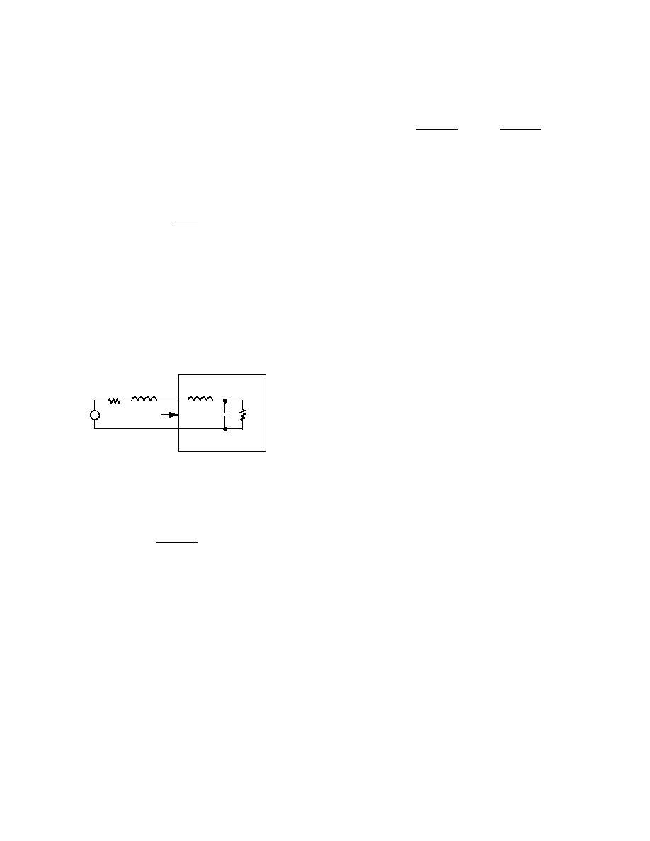
SYSTEM INSTABILITY CONSIDERATIONS
In a distributed power supply architecture, a power source
provides power to many "point-of-load" (POL) converters. At
low frequencies, the POL converters appear incrementally as
negative resistance loads. This negative resistance could cause
system instability problems.
≠12≠
ADDC02812DA/ADDC02815DA
REV. A
Incremental Negative Resistance: A POL converter is designed
to hold its output voltage constant no matter how its input volt-
age varies. Given a constant load current, the power drawn from
the input bus is therefore also a constant. If the input voltage
increases by some factor, the input current must decrease by the
same factor to keep the power level constant. In incremental
terms, a positive incremental change in the input voltage results
in a negative incremental change in the input current. The POL
converter therefore looks, incrementally, as a negative resistor.
The value of this negative resistor at a particular operating
point, V
IN
, I
IN
, is:
R
N
=
≠V
IN
I
IN
Note that this resistance is a function of the operating point. At
full load and low input line, the resistance is its smallest, while
at light load and high input line, it is its largest.
Potential System Instability: The preceding analysis assumes
dc voltages and currents. For ac waveforms the incremental input
model for the POL converter must also include the effects of its
input filter and control loop dynamics. When the POL con-
verter is connected to a power source, modeled as a voltage
source, V
S
, in series with an inductor, L
S
, and some positive
resistor, R
S
, the network of Figure 25 results.
L
P
C
P
≠|R
N
|
ADI DC/DC CONVERTER
L
S
R
S
V
S
INPUT
TERMINALS
Figure 25. Model of Power Source and POL Converter
Connection
The network shown in Figure 25 is second order and has the
following characteristic equation:
s
2
(L
S
+
L
P
)C
+
s
(L
S
+
L
P
)
≠|R
N
|
+
R
S
C
P
+
1
=
0
For the power delivery to be efficient, it is required that R
S
<<
R
N
. For the system to be stable, however, the following relation-
ship must hold:
C
P
|R
N
|
>
(L
S
+
L
P
)
R
S
or R
S
>
(L
S
+
L
P
)
C
P
|R
N
|
Notice from this result that if (L
S
+ L
P
) is too large, or if R
S
is
too small, the system might be unstable. This condition would
first be observed at low input line and full load since the abso-
lute value of R
N
is smallest at this operating condition.
If an instability results and it cannot be corrected by changing
L
S
or R
S
, such as during the MIL-STD-461D tests due to the
LISN requirement, one possible solution is to place a capacitor
across the input of the POL converter. Another possibility is to
place a small resistor in series with this extra capacitor.
The analysis so far has assumed the source of power was a volt-
age source (e.g., a battery) with some source impedance. In
some cases, this source may be the output of a front-end (FE)
converter. Although each FE converter is different, a model for
a typical one would have an LC output filter driven by a voltage
source whose value was determined by the feedback loop. The
LC filter usually has a high Q, so the compensation of the feed-
back loop is chosen to help dampen any oscillations that result
from load transients. In effect, the feedback loop adds "positive
resistance" to the LC network.
When the POL converter is connected to the output of this FE
converter, the POL's "negative resistance" counteracts the
effects of the FE's "positive resistance" offered by the feedback
loop. Depending on the specific details, this might simply mean
that the FE converter's transient response is slightly more oscil-
latory, or it may cause the entire system to be unstable.
For the ADDC02812DA and ADDC02815DA, L
P
is approxi-
mately 1
µ
H and C
P
is approximately 4
µ
F. Figure 12 shows a
more accurate depiction of the input impedance of the converter
as a function of frequency. The negative resistance is, itself, a
very good incremental model for the power state of the con-
verter for frequencies into the several kHz range (see Figure 12).

ADDC02812DA/ADDC02815DA
REV. A
≠13≠
NAVMAT DERATING
NAVMAT is a Navy power supply reliability manual that is
frequently cited by specifiers of power supplies. A key section of
NAVMAT P4855-1A discusses guidelines for derating designs
and their components. The two key derating criteria are voltage
derating and power derating. Voltage derating is done to reduce
the possibility of electrical breakdown, whereas power derating
is done to maintain the component material below a specified
maximum temperature. While power deratings are typically stated
in terms of current limits (e.g., derate to x% of maximum rating),
NAVMAT also specifies a maximum junction temperature of the
semiconductor devices in a power supply. The NAVMAT
component deratings applicable to the ADDC02812DA and
ADDC02815DA are as follows:
Resistors
80% voltage derating
50% power derating
Capacitors
50% voltage and ripple voltage derating
70% ripple current derating
Transformers and Inductors
60% continuous voltage and current derating
90% surge voltage and current derating
20
∞
C less than rated core temperature
30
∞
C below insulation rating for hot spot temperature
25% insulation breakdown voltage derating
40
∞
C maximum temperature rise
Transistors
50% power derating
60% forward current (continuous) derating
75% voltage and transient peak voltage derating
110
∞
C maximum junction temperature
Diodes (Switching, General Purpose, Rectifiers)
70% current (surge and continuous) derating
65% peak inverse voltage derating
110
∞
C maximum junction temperature
Diodes (Zeners)
70% surge current derating
60% continuous current derating
50% power derating
110
∞
C maximum junction temperature
Microcircuits (Linears)
70% continuous current derating
75% signal voltage derating
110
∞
C maximum junction temperature
The ADDC02812DA and ADDC02815DA, with one excep-
tion, can meet all the derating criteria listed above. However,
there are a few areas of the NAVMAT deratings where meeting
the guidelines unduly sacrifices performance of the circuit.
Therefore, the standard unit makes the following exceptions.
Common-Mode EMI Filter Capacitors: The standard
supply uses 500 V capacitors to filter common-mode EMI.
NAVMAT guidelines would require 1000 V capacitors to meet
the 50% voltage derating (500 V dc input to output isolation),
resulting in less common-mode capacitance for the same space.
In typical electrical power supply systems, where the load
ground is eventually connected to the source ground, common-
mode voltages never get near the 500 V dc rating of the stan-
dard supply. Therefore, a lower voltage rating capacitor (500 V)
was chosen to fit more capacitance in the same space in order to
better meet the conducted emissions requirement of MIL-STD-
461D (CE102). For those applications which require 250 V or
less of isolation from input to output, the present designs would
meet NAVMAT guidelines.
Switching Transistors: 100 V MOSFETs are used in the
standard unit to switch the primary side of the transformers.
Their nominal off-state voltage meets the NAVMAT derating
guidelines. When the MOSFETs are turned off, however,
momentary spikes occur that reach 100 V. The present genera-
tion of MOSFETs are rated for repetitive avalanche, a condition
that was not considered by the NAVMAT deratings. In the
worst case condition, the energy dissipated during avalanche is
1% of the device's rated repetitive avalanche energy. To meet
the NAVMAT derating, 200 V MOSFETs could be used. The
100 V MOSFETs are used instead for their lower on-state resis-
tance, resulting in higher efficiency for the power supply.
Output Rectifiers (ADDC02815DA only): Schottky diodes
are used as output rectifiers for the
±
15 V dc converter. The
reverse voltage stress on these diodes under normal operating
conditions is 75% of their maximum rating, compared to a
NAVMAT derating guideline of 65%.

≠14≠
ADDC02812DA/ADDC02815DA
REV. A
It should be noted that there are several areas of ambiguity with
respect to CE102 measurements that may concern the systems
engineer. One area of ambiguity in this measurement is the
nature of the load. If it is constant, then the ripple voltage on
the converter's input leads is due only to the operation of the
converter. If, on the other hand, the load is changing over time,
this variation causes an additional input current and voltage
ripple to be drawn at the same frequency. If the frequency is
high enough, the converter's filter will help attenuate this sec-
ond source of ripple, but if it is below approximately 100 kHz, it
will not. The system may then not meet the CE102 require-
ment, even though the converter is not the source of the EMI.
If this is the case, additional capacitance may be needed across
the load or across the input to the converter.
Another ambiguity in the CE102 measurement concerns
common-mode voltage. If the load is left unconnected from the
ground plane (even though the case is grounded), the common-
mode ripple voltages will be smaller than if the load is grounded.
The test specifications do not state which procedure should be
used. However, in neither case (load grounded or floating) will
the typical EMI test setup described below be exactly represen-
tative of the final system configuration EMI test. For the follow-
ing reasons, the same is true if separately packaged EMI filters
are used.
In almost all systems the output ground of the converter is ulti-
mately connected to the input ground of the system. The para-
sitic capacitances and inductances in this connection will affect
the common-mode voltage and the CE102 measurement. In
addition, the inductive impedance of this ground connection
can cause resonances, thereby affecting the performance of the
common-mode filter in the power supply.
In response to these ambiguities, the Analog Devices converter
has been tested for CE102 under a constant load and with the
output ground floating. While these measurements are a good
indication of how the converter will operate in the final system
configuration, the user should confirm CE102 testing in the
final system configuration.
CE101: This test measures emissions on the input leads in the
frequency range between 30 Hz and 10 kHz. The intent of this
requirement is to ensure that the dc/dc converter does not corrupt
the power quality (allowable voltage distortion) on the power
buses present on the platform. There are several CE101 limit
curves in MIL-STD-461D. The most stringent one applicable for
the converter is the one for submarine applications. Figure 13
shows that the converter easily meets this requirement (the return
line measurement is similar). The components at 60 Hz and its
harmonics are a result of ripple in the output of the power
source used to supply the converter.
NAVMAT Junction Temperatures: The two types of power
deratings (current and temperature) can be independent of one
another. For instance, a switching diode can meet its derating of
70% of its maximum current, but its junction temperature can
be higher than 110
∞
C if the case temperature of the converter,
which is not controlled by the manufacturer, is allowed to go
higher. Since some users may choose to operate the power sup-
ply at a case temperature higher than 90
∞
C, it then becomes
important to know the temperature rise of the hottest semicon-
ductors. This is covered in the specification table in the section
entitled "Thermal Characteristics."
EMI CONSIDERATIONS
The ADDC02812DA and ADDC02815DA have an integral
differential- and common-mode EMI filter that is designed to
meet all applicable requirements in MIL-STD-461D when the
power converter is installed in a typical system setup (described
below). The converter also contains transient protection cir-
cuitry that permits the unit to survive short, high voltage tran-
sients across its input power leads. The purpose of this section is
to describe the various MIL-STD-461D tests and the converter's
corresponding performance. Consult factory for additional
information.
The figures and tests referenced herein were obtained from
measurements on the ADDC02805SA, a single 5 V dc output
converter. Since the construction and topology of the dual out-
put converters are almost identical to the single output con-
verter, and the component values of the EMI differential and
common filter in the dual output converters are identical to the
single output converter, the text references these figures and
tests as typical of the ADDC02812DA and ADDC02815DA
converters.
Electromagnetic interference (EMI) is governed by MIL-STD-
461D, which establishes design requirements, and MIL-STD-
462D, which defines test methods. EMI requirements are
categorized as follows (xxx designates a three digit number):
∑ CExxx: conducted emissions (EMI produced internal to the
power supply which is conducted externally through its input
power leads)
∑ CSxxx: conducted susceptibility (EMI produced external
to the power supply which is conducted internally through
the input power leads and may interfere with the supply's
operation)
∑ RExxx: radiated emissions (EMI produced internal to the
power supply which is radiated into the surrounding space)
∑ RSxxx: radiated susceptibility (EMI produced external to the
power supply which radiates into or through the power supply
and may interfere with its proper operation)

ADDC02812DA/ADDC02815DA
REV. A
≠15≠
CE102: This test measures emissions in the frequency range
between 10 kHz and 10 MHz. The measurements are made on
both of the input leads of the converter which are connected to
the power source through LISNs. The intent of this requirement
in the lower frequency portion of the requirement is to ensure
that the dc/dc converter does not corrupt the power quality
(allowable voltage distortion) on the power buses present on the
platform. At higher frequencies, the intent is to serve as a sepa-
rate control from RE102 on potential radiation from power
leads which may couple into sensitive electronic equipment.
Figure 14 shows the CE102 limit and the measurement taken
from the +V
IN
line. While the measurement taken from the
input return line is slightly different, both comfortably meet the
MIL-STD-461D, CE102 limit.
CS101: This test measures the ability of the converter to reject
low frequency differential signals, 30 Hz to 50 kHz, injected on
the dc inputs. The measurement is taken on the output power
leads. The intent is to ensure that equipment performance is not
degraded from ripple voltages associated with allowable dis-
tortion of power source voltage waveforms. Figure 10 shows a
typical audio susceptibility graph. Note that according to the
MIL-STD-461D test requirements, the injected signal between
30 Hz and 5 kHz has an amplitude of 2 V rms and from 5 kHz
to 50 kHz the amplitude decreases inversely with frequency to
0.2 V rms. The curve of the injected signal should be multiplied
by the audio susceptibility curve to determine the output ripple
at any frequency. When this is done, the worst case output
ripple at the frequency of the input ripple occurs at 5 kHz, at
which point there is typically a 25 mV peak-to-peak output
ripple.
It should be noted that MIL-STD-704 has a more relaxed
requirement for rejection of low frequency differential signals
injected on the dc inputs than MIL-STD-461D. MIL-STD-
704 calls for a lower amplitude ripple to be injected on the input
in a narrower frequency band, 10 Hz to 20 kHz.
CS114: This test measures the ability of the converter to operate
correctly during and after being subjected to currents injected
into bulk cables in the 10 kHz to 400 MHz range. Its purpose is
to simulate currents that would be developed in these cables due
to electromagnetic fields generated by antenna transmissions.
The converter is designed to meet the requirements of this test
when the current is injected on the input power leads cable.
Consult factory for more information.
CS115: This test measures the ability of the converter to oper-
ate correctly during and after being subjected to 30 ns long
pulses of current injected into bulk cables. Its purpose is to
simulate transients caused by lightning or electromagnetic
pulses. The converter is designed to meet this requirement
when applied to its input power leads cable. Consult factory for
more information.
CS116: This test measures the ability of the converter to oper-
ate correctly during and after being subjected to damped sinu-
soid transients in the 10 kHz to 100 MHz range. Its purpose is
to simulate current and voltage waveforms that would occur
when natural resonances in the system are excited. The con-
verter is designed to meet this requirement when applied to its
input power leads cable. Consult factory for more information.
RE101: This requirement limits the strength of the magnetic
field created by the converter in order to avoid interference with
sensitive equipment located nearby. The measurement is made
from 30 Hz to 100 kHz. The most stringent requirement is for
the Navy. Figure 15 shows the test results when the pickup coil
is held 7 cm above the converter. As can be seen, the converter
easily meets this requirement.
RE102: This requirements limits the strength of the electric
field emissions from the power converter to protect sensitive
receivers from interference. The measurement is made from
10 kHz to 18 GHz with the antenna oriented in the vertical
plane. For the 30 MHz and above range the standard calls for
the measurement to be made with the antenna oriented in the
horizontal plane, as well.
In a typical power converter system setup, the radiated emis-
sions can come from two sources: (1) the input power leads as
they extend over the two meter distance between the LISNs and
the converter, as required for this test, and (2) the converter
output leads and load. The latter is likely to create significant
emissions if left uncovered since minimal EMI filtering is pro-
vided at the converter's output. It is typical, however, that the
power supply and its load would be contained in a conductive
enclosure in applications where this test is applicable. A metal
screen enclosure was therefore used to cover the converter and
its load for this test.

≠16≠
ADDC02812DA/ADDC02815DA
REV. A
Figure 16 shows test results for the vertical measurement and
compares them against the most stringent RE102 requirement;
the horizontal measurement (30 MHz and above) was similar.
As can be seen, the emissions just meet the standard in the
18 MHz≠28 MHz range. This component of the emissions is
due to common-mode currents flowing through the input power
leads. As mentioned in the section on CE102 above, the level of
common-mode current that flows is dependent on how the load
is connected. This measurement is therefore a good indication
of how well the converter will perform in the final configuration,
but the user should confirm RE102 testing in the final system.
RS101: This requirement is specialized and is intended to
check for sensitivity to low frequency magnetic fields in the
30 Hz to 50 kHz range. The converter is designed to meet this
requirement. Consult factory for more information.
RS103: This test calls for correct operation during and after the
unit under test is subjected to radiated electric fields in the
10 kHz to 40 GHz range. The intent is to simulate electro-
magnetic fields generated by antenna transmissions. The con-
verter is designed to meet this requirement. Consult factory for
more information.
Circuit Setup for EMI Test
Figure 17 shows a schematic of the test setup used for the EMI
measurements discussed above. The output of the converter is
connected to a resistive load designed to draw full power. There
is a 0.1
µ
F capacitor placed across this resistor that typifies
by-pass capacitance normally used in this application. At the
input of the converter there are two differential capacitors (the
larger one having a series resistance) and two small common-
mode capacitors connected to case ground. The case itself was
connected to the metal ground plane in the test chamber. For
the RE102 test, a metal screen box was used to cover both the
converter and its load (but not the two meters of input power
lead cables). This box was also electrically connected to the
metal ground plane.
With regard to the components added to the input power lines,
the 100
µ
F capacitor with its 1
series resistance is required to
achieve system stability when the unit is powered through the
LISNs, as the MIL-STD-461D standard requires. These LISNs
have a series inductance of 50
µ
H at low frequencies, giving a
total differential inductance of 100
µ
H. As explained earlier in
the System Instability section, such a large series source induc-
tance will cause an instability as it interacts with the converter's
negative incremental input resistance unless some corrective
action is taken. The 100
µ
F capacitor and 1
resistor provide
the stabilization required.
It should be noted that the values of these stabilization compo-
nents are appropriate for a single converter load. If the system
makes use of several converters, the values of the components
will need to be changed slightly, but not such that they are
repeated for every converter. It should also be noted that most
system applications will not have a source inductance as large as
the 100
µ
H built into the LISNs. For those systems, a much
smaller input capacitor could be used.
The 2
µ
F differential-mode capacitor and the two 82 nF common-
mode capacitors were added to achieve the results shown in the
EMI measurement figures described above.
RELIABILITY CONSIDERATIONS
MTBF (Mean Time Between Failure) is a commonly used
reliability concept that applies to repairable items in which
failed elements are replaced upon failure. The expression for
MTBF is
MTBF = T/r
where
T = total operating time
r = number of failures
In lieu of actual field data, MTBF can be predicted per
MIL-HDBK-217.
MTBF, Failure Rate and Probability of Failure: A proper
understanding of MTBF begins with its relationship to lambda
( ), which is the failure rate. If a constant failure rate is assumed,
then MTBF = 1/ , or = 1/MTBF. If a power supply has an
MTBF of 1,000,000 hours, this does not mean it will last
1,000,000 hours before it fails. Instead, the MTBF describes the
failure rate. For 1,000,000 hours MTBF, the failure rate during
any hour is 1/1,000,000, or 0.0001%. Thus, a power supply
with an MTBF of 500,000 hours would have twice the failure
rate (0.0002%) of one with 1,000,000 hours.
ADDC02812DA/ADDC02815DA
REV. A
≠17≠
What users should be interested in is the probability of a power
supply not failing prior to some time t. Given the assumption of
a constant failure rate, this probability is defined as
R(t )
=
e
≠
t
where R(t) is the probability of a device not failing prior to some
time, t.
If we substitute = 1/MTBF in the above formula, then the
expression becomes
R(t )
=
e
≠t
MTBF
This formula is the correct way to interpret the meaning of
MTBF.
If we assume t = MTBF = 1,000,000 hours, then the probability
that a power supply will not fail prior to 1,000,000 hours of use
is e
≠1
, or 36.8%. This is quite different from saying the power
supply will last 1,000,000 hours before it fails. The probability
that the power supply will not fail prior to 50,000 hours of use is
e
≠.05
, or 95%. For t = 10,000 hours, the probability of no failure
is e
≠.01
, or 99%.
Temperature and Environmental Factors: Although the
calculation of MTBF per MIL-HDBK-217 is a detailed process,
there are two key variables that give the manufacturer significant
leeway in predicting an MTBF rating. These two variables are
temperature and environmental factor. Therefore, for users to
properly compare MTBF numbers from two different manufac-
turers, the environmental factor and the temperature must be
identical. Contact the factory for MTBF calculations for specific
environmental factors and temperatures.
MECHANICAL CONSIDERATIONS
When mounting the converter into the next higher level assem-
bly, it is important to insure good thermal contact is made
between the converter and the external heat sink. Poor thermal
connection can result in the converter shutting off, due to the
temperature shutdown feature (Pin 9), or reduced reliability for
the converter due to higher than anticipated junction and case
temperatures. For these reasons the mounting tab locations
were selected to insure good thermal contact is made near the
hot spots of the converter which are shown in the shaded areas
of Figure 26.
Figure 26. Hot Spots (Shaded Areas) of DC/DC Converter
The pins of the converter are typically connected to the next
higher level assembly by bending them at right angles, either
down or up, and cutting them shorter for insertion in printed
circuit board through holes. In order to maintain the hermetic
integrity of the seals around the pins, a fixture should be used
for bending the pins without stressing the pin-to-sidewall seals.
It is recommended that the minimum distance between the
package edge and the inside of the pin be 100 mils (2.54 mm)
for the 40 mil (1.02 mm) diameter pins; 120 mils (3.05 mm)
from the package edge to the center of the pin as shown in
Figure 27.
0.100"
(2.54mm)
0.120"
(3.05mm)
Figure 27. Minimum Bend Radius of 40 Mil (1.02 mm) Pins
≠18≠
ADDC02812DA/ADDC02815DA
REV. A
≠18≠
Note: The value of C1 is dependent on source impedance.
Refer to section on System Instability Considerations. The remote
sense connection shown in Figure 29 was selected to reference
STATUS to the output ground of the load. If the resistive drop
in the positive V
OUT
connection to the load is sufficiently large
compared to the negative V
OUT
connection to the load, then
connect Pin 1 to the output return of the converter and Pin 2
to the +V
OUT
. However, STATUS, which is referenced to
≠SENSE (Pin 1), will not be referenced to the output ground of
the load.
1
2
10
11
17
16
15
14
13
12
ADDC02812DA/
ADDC02815DA
+28VDC
28RTN
≠R
LOAD
+R
LOAD
C1
NOTE: VALUE OF C1 IS DEPENDENT ON SOURCE IMPEDANCE.
REFER TO SECTION ON SYSTEM INSTABILITY CONSIDERATIONS.
Figure 28. Typical Power Connections and External Parts
for Converter
1
2
10
11
17
16
15
14
13
12
ADDC02812DA/
ADDC02815DA
+28VDC
28RTN
R
LOAD
C1
NOTE: VALUE OF C1 IS DEPENDENT ON SOURCE IMPEDANCE.
REFER TO SECTION ON SYSTEM INSTABILITY CONSIDERATIONS.
Figure 29. Typical Connections for Providing 24 V Output/
30 V Output from ADDC02812DA/ADDC02815DA Re-
spectively
ADDC02812DA/ADDC02815DA
REV. A
≠19≠
NOMINAL CASE DIMENSIONS IN INCHES AND (mm)
[All tolerances
±
0.005" (
±
0.13 mm) unless otherwise specified]
0.150 (3.81)
0.100 (2.54)
8 PLCS
0.200 (5.08)
0.150 (3.81)
0.200 (5.08)
0.390 0.010
(9.91 0.25)
0.800 0.010
(20.32 0.25)
1.145 (29.08)
2 PLCS
0.150 (3.81)
4 PLCS
TOP VIEW
0.149 (3.78)
DIA TYP
0.300 (7.62) SQ
0.010
4 PLCS
0.200 (5.08) 5 PLCS
0.250 (6.35)
2 PLCS
1.500 0.010
(38.10 0.25)
0.040 0.003
(1.02 0.08)
0.090 0.010
(2.29 0.25)
4 PLCS
2.745 0.010
(69.72 0.25)
1.800
(45.72)
TYP
2.100 0.010
(53.34 0.25)
NOTES
1
The final product weight is 85 grams maximum.
2
The package base material if made of molybdenum and is nominally 40 mils (1.02 mm) thick. The "runout" is less than 2 mils per inch (0.02 mm per cm).
3
The high current pins (10≠17) are 40 mil (1.02 mm) diameter; are 99.8% copper; and are plated with gold over nickel.
4
The signal carrying pins (1≠9) are 18 mil (0.46 mm) diameter; are Kovar; and are plated with gold over nickel.
5
All pins are a minimum length of 0.740 inches (18.80 mm) when the product is shipped. The pins are typically bent up or down and cut shorter for proper connec-
tion into the user's system.
6
All pin-to-sidewall spacings are guaranteed for a minimum of 500 V dc breakdown at standard air pressure.
7
The case outline was originally designed using the inch-pound units of measurement. In the event of conflict between the metric and inch-pound units, the inch-
pound shall take precedence.
Screening Levels for ADDC02812DA AND ADDC02815DA
Screening Steps
Industrial (KV)
Ruggedized Industrial (TV)
MIL-STD-883B/SMD (TV/QMLH)
Pre-Cap Visual
100%
MIL-STD-883, TM2017
Temp Cycle
N/A
N/A
Constant Acceleration
N/A
N/A
Fine Leak
Guaranteed to Meet
Guaranteed to Meet
MIL-STD-883, TM1014
MIL-STD-883, TM1014
Compliant to MIL-PRF-38534
Gross Leak
Guaranteed to Meet
Guaranteed to Meet
MIL-STD-883, TM1014
MIL-STD-883, TM1014
Burn-In
N/A
MIL-STD-883, TM1015,
96 Hrs at +115
∞
C Case
Final Electrical Test
At +25
∞
C, Per Specification
At +25
∞
C, Per Specification
Table
Table

≠20≠
C2133a≠4≠12/97
PRINTED IN U.S.A.