AD7892
a
LC
2
MOS Single Supply,
12-Bit 600 kSPS ADC
FUNCTIONAL BLOCK DIAGRAM
REF OUT/REF IN
V
DD
+2.5V
REFERENCE
2k
12-BIT
ADC
TRACK/HOLD
SIGNAL
SCALING
AD7892
MODE
DB0
DB2
DB10/LOW
DB11/LOW
DGND
AGND
CONTROL LOGIC
CONVST
EOC
RD
CS
V
IN1
V
IN2
CLOCK
DB3/
RFS
DB4/SCLK
DB5/SDATA
STANDBY
The AD7892 is fabricated in Analog Devices' Linear Compat-
ible CMOS (LC
2
MOS) process, a mixed technology process
that combines precision bipolar circuits with low power CMOS
logic. It is available in a 24-lead, 0.3" wide, plastic or hermetic
DIP or in a 24-lead SOIC.
PRODUCT HIGHLIGHTS
1. The AD7892-3 features a conversion time of 1.47
µs and a
track/hold acquisition time of 200 ns. This allows a through-
put rate for the part up to 600 kSPS. The AD7892-1 and
AD7892-2 operate with throughput rates of 500 kSPS.
2. The AD7892 operates from a single +5 V supply and con-
sumes 60 mW typ making it ideal for low power and portable
applications.
3. The part offers a high speed, flexible interface arrangement
with parallel and serial interfaces for easy connection to
microprocessors, microcontrollers and digital signal
processors.
GENERAL DESCRIPTION
The AD7892 is a high speed, low power, 12-bit A/D converter
that operates from a single +5 V supply. The part contains a
1.47
µs successive approximation ADC, an on-chip track/hold
amplifier, an internal +2.5 V reference and on-chip versatile
interface structures that allow both serial and parallel connec-
tion to a microprocessor. The part accepts an analog input range
of
±10 V or ±5 V (AD7892-1), 0 V to +2.5 V (AD7892-2) and
±2.5 V (AD7892-3). Overvoltage protection on the analog inputs
for the AD7892-1 and AD7892-3 allows the input voltage to go
to
±17 V or ±7 V respectively without damaging the ports.
The AD7892 offers a choice of two data output formats: a
single, parallel, 12-bit word or serial data. Fast bus access times
and standard control inputs ensure easy parallel interface to
microprocessors and digital signal processors. A high speed
serial interface allows direct connection to the serial ports of
microcontrollers and digital signal processors.
In addition to the traditional dc accuracy specifications such as
linearity, full-scale and offset errors, the part is also specified for
dynamic performance parameters including harmonic distortion
and signal-to-noise ratio.
REV. C
Information furnished by Analog Devices is believed to be accurate and
reliable. However, no responsibility is assumed by Analog Devices for its
use, nor for any infringements of patents or other rights of third parties
which may result from its use. No license is granted by implication or
otherwise under any patent or patent rights of Analog Devices.
FEATURES
Fast 12-Bit ADC with 1.47
s Conversion Time
600 kSPS Throughput Rate (AD7892-3)
500 kSPS Throughput Rate (AD7892-1, AD7892-2)
Single Supply Operation
On-Chip Track/Hold Amplifier
Selection of Input Ranges:
10 V or 5 V for AD7892-1
0 V to +2.5 V for AD7892-2
2.5 V for AD7892-3
High Speed Serial and Parallel Interface
Low Power, 60 mW typ
Overvoltage Protection on Analog Inputs (AD7892-1
and AD7892-3)
One Technology Way, P.O. Box 9106, Norwood, MA 02062-9106, U.S.A.
Tel: 781/329-4700
World Wide Web Site: http://www.analog.com
Fax: 781/326-8703
© Analog Devices, Inc., 2000

(V
DD
= +5 V 5%, AGND = DGND = 0 V, REF IN = +2.5 V. All specifications T
MIN
to T
MAX
unless otherwise noted.)
AD7892≠SPECIFICATIONS
Parameter
A Versions
1
B Versions
S Version
2
Unit
Test Conditions/Comments
DYNAMIC PERFORMANCE
AD7892-1, AD7892-2
f
IN
= 100 kHz. f
SAMPLE
= 500 kSPS
Signal to (Noise + Distortion) Ratio
3
70
70
70
dB min
Total Harmonic Distortion
3
≠78
≠78
≠78
dB max
typ ≠84 dB
Peak Harmonic or Spurious Noise
3
≠79
≠79
≠79
dB max
Intermodulation Distortion
3
fa = 49 kHz, fb = 50 kHz
2nd Order Terms
≠78
≠78
≠78
dB max
typ ≠84 dB
3rd Order Terms
≠78
≠78
≠78
dB max
typ ≠84 dB
AD7892-3
f
IN
= 100 kHz. f
SAMPLE
= 600 kSPS
Signal to (Noise + Distortion) Ratio
3
70
70
dB min
Total Harmonic Distortion
3
≠78
≠78
dB max
Peak Harmonic or Spurious Noise
3
≠79
≠79
dB max
Intermodulation Distortion
3
fa = 49 kHz, fb = 50 kHz
2nd Order Terms
≠78
≠78
dB max
3rd Order Terms
≠78
≠78
dB max
DC ACCURACY
Resolution
12
12
12
Bits
Minimum Resolution for Which No
Missing Codes Are Guaranteed
12
12
12
Bits
Relative Accuracy
3
±1.5
±1
±1
LSB max
Differential Nonlinearity
3
±1
±1
±1
LSB max
AD7892-1
Positive Full-Scale Error
3
±4
±4
±5
LSB max
Negative Full-Scale Error
3
±4
±4
±5
LSB max
Bipolar Zero Error
3
±3
±2
±3
LSB max
AD7892-3
Positive Full-Scale Error
3
±4
±4
LSB max
Negative Full-Scale Error
3
±4
±4
LSB max
Bipolar Zero Error
3
±4
±3
LSB max
AD7892-2
Positive Full-Scale Error
3
±5
±5
±5
LSB max
Unipolar Offset Error
3
±4
±3
±4
LSB max
ANALOG INPUT
AD7892-1
Input Voltage Range
±10
±10
±10
Volts
Input Applied to V
IN1
with V
IN2
Grounded
Input Voltage Range
±5
±5
±5
Volts
Input Applied to V
IN1
and V
IN2
Input Resistance
8
8
8
k
min
Input Applied to V
IN1
with V
IN2
Grounded
AD7892-2
Input Voltage Range on V
IN1
0 to +2.5
0 to +2.5
0 to +2.5
Volts
Input Applied to V
IN1
Input Current
10
10
50
nA max
Input Voltage Range on V
IN2
±50
±50
±50
mV max
AD7892-3
Input Voltage Range on V
IN1
±2.5
±2.5
Volts
Input Applied to V
IN1
Input Resistance
2
2
k
min
REFERENCE OUTPUT/INPUT
REF IN Input Voltage Range
2.375/2.625
2.375/2.625
2.375/2.625
V min/V max
2.5 V
± 5%
Input Impedance
1.6
1.6
1.6
k
min
Resistor Connected to Internal Reference Node
Input Capacitance
4
10
10
10
pF max
REF OUT Output Voltage
2.5
2.5
2.5
V nom
REF OUT Error @ +25
∞C
±10
±10
±10
mV max
T
MIN
to T
MAX
±20
±20
±25
mV max
REF OUT Temperature Coefficient
25
25
25
ppm/
∞C typ
REF OUT Output Impedance
5.5
5.5
5.5
k
nom
LOGIC INPUTS
Input High Voltage, V
INH
2.4
2.4
2.4
V min
V
DD
= 5 V
± 5%
Input Low Voltage, V
INL
0.8
0.8
0.8
V max
V
DD
= 5 V
± 5%
Input Current, I
IN
±10
±10
±10
µA max
V
IN
= 0 V to V
DD
Input Capacitance, C
IN
4
10
10
10
pF max
≠2≠
REV. C

ABSOLUTE MAXIMUM RATINGS*
(T
A
= +25
∞C unless otherwise noted)
V
DD
to AGND . . . . . . . . . . . . . . . . . . . . . . . . . ≠0.3 V to +7 V
V
DD
to DGND . . . . . . . . . . . . . . . . . . . . . . . . . ≠0.3 V to +7 V
Analog Input Voltage to AGND
AD7892-1 . . . . . . . . . . . . . . . . . . . . . . . . . . . . . . . . .
±17 V
AD7892-2 . . . . . . . . . . . . . . . . . . . . . . . . . . . . ≠0.3 V, V
DD
AD7892-3 . . . . . . . . . . . . . . . . . . . . . . . . . . . . . . . . . .
±7 V
Reference Input Voltage to AGND . . . ≠0.3 V to V
DD
+ 0.3 V
Digital Input Voltage to DGND . . . . . ≠0.3 V to V
DD
+ 0.3 V
Digital Output Voltage to DGND . . . . ≠0.3 V to V
DD
+ 0.3 V
Operating Temperature Range
Commercial (A, B Versions) . . . . . . . . . . . ≠40
∞C to +85∞C
Extended (S Version) . . . . . . . . . . . . . . . . ≠55
∞C to +125∞C
Storage Temperature Range . . . . . . . . . . . . ≠65
∞C to +150∞C
Parameter
A Versions
1
B Versions
S Version
2
Unit
Test Conditions/Comments
LOGIC OUTPUTS
Output High Voltage, V
OH
4.0
4.0
4.0
V min
I
SOURCE
= 200
µA
Output Low Voltage, V
OL
0.4
0.4
0.4
V max
I
SINK
= 1.6 mA
DB11≠DB0
Floating-State Leakage Current
±10
±10
±10
µA max
Floating-State Capacitance
4
15
15
15
pF max
Output Coding
AD7892-1 and AD7892-3
Two's Complement
AD7892-2
Straight (Natural) Binary
CONVERSION RATE
Conversion Time
1.47
1.47
µs max
AD7892-3
Track/Hold Acquisition Time
3
0.2
0.2
µs max
AD7892-3
Conversion Time
1.6
1.6
1.68
µs max
AD7892-1 and AD7892-2
Track/Hold Acquisition Time
3
0.4
0.4
0.32
µs max
AD7892-1 and AD7892-2
POWER REQUIREMENTS
V
DD
+5
+5
+5
V nom
±5% for Specified Performance
I
DD
5
Normal Operation
18
18
19
mA max
Standby Mode
6
AD7892-2
250
250
µA typ
AD7892-3, AD7892-1
80
80
100
µA max
typ 15
µA
Power Dissipation
5
Normal Operation
90
90
95
mW max
V
DD
= +5 V. Typically 60 mW
Standby Mode
6
AD7892-2
1.25
1.25
mW typ
AD7892-3, AD7892-1
400
400
500
µW max
V
DD
= +5 V. Typically 75
µW
NOTES
1
Temperature ranges are as follows: A, B Versions: ≠40
∞C to +85∞C; S Version: ≠55∞C to +125∞C.
2
S Version available on AD7892-1 and AD7892-2 only.
3
See Terminology.
4
Sample tested @ +25
∞C to ensure compliance.
5
These normal mode and standby mode currents are achieved with resistors (in the range 10 k
to 100 k) to either DGND or V
DD
on Pins 8, 9, 16 and 17.
6
A conversion should not be initiated on the part within 30
µs of exiting standby mode.
Specifications subject to change without notice.
AD7892
Junction Temperature . . . . . . . . . . . . . . . . . . . . . . . . . +150
∞C
Plastic DIP Package, Power Dissipation . . . . . . . . . . 450 mW
JA
Thermal Impedance . . . . . . . . . . . . . . . . . . . . . 105
∞C/W
Lead Temperature (Soldering, 10 sec) . . . . . . . . . . . +260
∞C
Cerdip Package, Power Dissipation . . . . . . . . . . . . . . 450 mW
JA
Thermal Impedance . . . . . . . . . . . . . . . . . . . . . . 70
∞C/W
Lead Temperature (Soldering, 10 sec) . . . . . . . . . . . +300
∞C
SOIC Package, Power Dissipation . . . . . . . . . . . . . . . 450 mW
JA
Thermal Impedance . . . . . . . . . . . . . . . . . . . . . . 75
∞C/W
Lead Temperature, Soldering
Vapor Phase (60 sec) . . . . . . . . . . . . . . . . . . . . . . +215
∞C
Infrared (15 sec) . . . . . . . . . . . . . . . . . . . . . . . . . . +220
∞C
*Stresses above those listed under Absolute Maximum Ratings may cause perma-
nent damage to the device. This is a stress rating only; functional operation of the
device at these or any other conditions above those listed in the operational
sections of this specification is not implied. Exposure to absolute maximum rating
conditions for extended periods may affect device reliability.
REV. C
≠3≠
AD7892
≠4≠
REV. C
TIMING CHARACTERISTICS
1, 2
A, B
S
Parameter
Versions
Version
Unit
Test Conditions/Comments
t
CONV
1.47
µs max
Conversion Time for AD7892-3
1.6
1.68
µs max
Conversion Time for AD7892-1, AD7892-2
t
ACQ
200
ns min
Acquisition Time for AD7892-3
400
320
ns min
Acquisition Time for AD7892-1, AD7892-2
Parallel Interface
t
1
35
45
ns min
CONVST Pulsewidth
t
2
60
60
ns min
EOC Pulsewidth
t
3
0
0
ns min
EOC Falling Edge to CS Falling Edge Setup Time
t
4
0
0
ns min
CS to RD Setup Time
t
5
35
45
ns min
Read Pulsewidth
t
6
3
35
40
ns max
Data Access Time After Falling Edge of
RD
t
7
4
5
5
ns min
Bus Relinquish Time After Rising Edge of
RD
30
40
ns max
t
8
0
0
ns min
CS to RD Hold Time
t
9
200
200
ns min
RD to CONVST Setup Time
Serial Interface
t
10
30
35
ns min
RFS Low to SCLK Falling Edge Setup Time
t
11
3
25
30
ns max
RFS Low to Data Valid Delay
t
12
25
25
ns min
SCLK High Pulsewidth
t
13
25
25
ns min
SCLK Low Pulsewidth
t
14
3
5
5
ns min
SCLK Rising Edge to Data Valid Hold Time
t
15
3
25
30
ns max
SCLK Rising Edge to Data Valid Delay
t
16
20
30
ns min
RFS to SCLK Falling Edge Hold Time
t
17
4
0
0
ns min
Bus Relinquish Time after Rising Edge of
RFS
30
30
ns max
t
17A
4
0
0
ns min
Bus Relinquish Time after Rising Edge of SCLK
30
30
ns max
NOTES
1
Sample tested at +25
∞C to ensure compliance. All input signals are measured with tr = tf = 1 ns (10% to 90% of +5 V) and timed from a voltage level of +1.6 V.
2
See Figures 2 and 3.
3
Measured with the load circuit of Figure 1 and defined as the time required for an output to cross 0.8 V or 2.4 V.
4
These times are derived from the measured time taken by the data outputs to change 0.5 V when loaded with the circuit of Figure 1. The measured number is then
extrapolated back to remove the effects of charging or discharging the 50 pF capacitor. This means that the times quoted in the timing characteristics are the true bus
relinquish times of the part and as such are independent of external bus loading capacitances.
5
Assumes CMOS loads on the data bits. With TTL loads, more current is drawn from the data lines and the
RD to CONVST time needs to be extended to 400 ns min.
Specifications subject to change without notice.
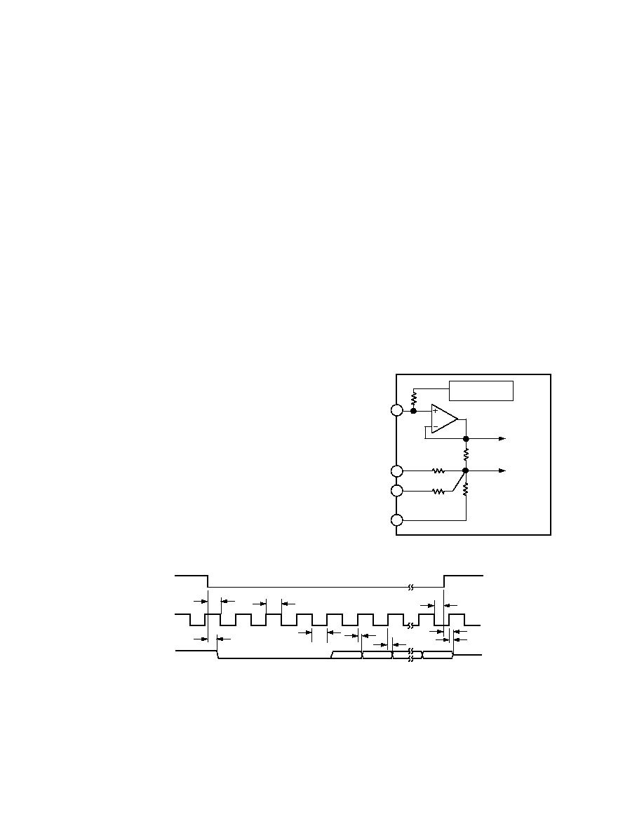
1.6mA
+1.6V
200 A
50pF
TO
OUTPUT
PIN
Figure 1. Load Circuit for Access Time and Bus Relinquish Time
CAUTION
ESD (electrostatic discharge) sensitive device. Electrostatic charges as high as 4000 V readily
accumulate on the human body and test equipment and can discharge without detection.
Although the AD7892 features proprietary ESD protection circuitry, permanent damage may
occur on devices subjected to high energy electrostatic discharges. Therefore, proper ESD
precautions are recommended to avoid performance degradation or loss of functionality.
(V
DD
= +5 V 5%, AGND = DGND = 0 V, REF IN = +2.5 V)
WARNING!
ESD SENSITIVE DEVICE
AD7892
REV. C
≠5≠
ORDERING GUIDE
Input
Sample
Relative
Temperature
Package
Model
Range
Rate
Accuracy
Range
Option
1
AD7892AN-1
±5 V or ±10 V
500 kSPS
≠40
∞C to +85∞C
N-24
AD7892BN-1
±5 V or ±10 V
500 kSPS
±1 LSB
≠40
∞C to +85∞C
N-24
AD7892AR-1
±5 V or ±10 V
500 kSPS
≠40
∞C to +85∞C
R-24
AD7892BR-1
±5 V or ±10 V
500 kSPS
±1 LSB
≠40
∞C to +85∞C
R-24
AD7892SQ-1
±5 V or ±10 V
500 kSPS
±1 LSB
≠55
∞C to +125∞C
Q-24
AD7892AN-2
0 V to +2.5 V
500 kSPS
≠40
∞C to +85∞C
N-24
AD7892BN-2
0 V to +2.5 V
500 kSPS
±1 LSB
≠40
∞C to +85∞C
N-24
AD7892AR-2
0 V to +2.5 V
500 kSPS
≠40
∞C to +85∞C
R-24
AD7892BR-2
0 V to +2.5 V
500 kSPS
±1 LSB
≠40
∞C to +85∞C
R-24
AD7892AN-3
±2.5 V
600 kSPS
≠40
∞C to +85∞C
N-24
AD7892BN-3
±2.5 V
600 kSPS
±1 LSB
≠40
∞C to +85∞C
N-24
AD7892AR-3
±2.5 V
600 kSPS
≠40
∞C to +85∞C
R-24
AD7892BR-3
±2.5 V
600 kSPS
±1 LSB
≠40
∞C to +85∞C
R-24
EVAL-AD7892-2CB
2
Evaluation Board
EVAL-AD7892-3CB
2
Evaluation Board
EVAL-CONTROL BOARD
3
Controller Board
NOTES
1
N = Plastic DIP; Q = Cerdip; R = SOIC.
2
These boards can be used as stand-alone evaluation boards or in conjunction with the EVAL-CONTROL BOARD for evaluation/demonstration purposes.
3
This board is a complete unit allowing a PC to control and communicate with all Analog Devices' evaluation boards ending in the CB designators.

AD7892
≠6≠
REV. C
PIN FUNCTION DESCRIPTION
Pin
No.
Mnemonic
Description
1
V
DD
Positive Supply Voltage, +5 V
± 5%.
2
STANDBY
Standby Input. Logic Input. With this input at a logic high, the part is in its normal operating
mode; with this input at a logic low, the part is placed in its standby or power-down mode, which
reduces power consumption to 5 mW typical.
3
V
IN2
Analog Input 2. For the AD7892-1, this input either connects to AGND or to V
IN1
to determine
the analog input voltage range. With V
IN2
connected to AGND on the AD7892-1, the analog input
range at the V
IN1
input is
±10 V. With V
IN2
connected to V
IN1
on the AD7892-1, the analog input
range to the part is
±5 V.
For the AD7892-2 and AD7892-3, this input can be left unconnected but must not be connected
to a potential other than AGND.
4
V
IN1
Analog Input 1. The analog input voltage to be converted by the AD7892 is applied to this input.
For the AD7892-1, the input voltage range is either
±5 V or ±10 V depending on where the V
IN2
input is connected. For the AD7892-2, the voltage range on the V
IN1
input is 0 V to +2.5 V with
respect to the voltage appearing at the V
IN2
input. For the AD7892-3, the voltage range on the V
IN1
input is
±2.5 V.
5
REF OUT/REF IN
Voltage Reference Output/Input. The part can be used with either its own internal reference or with
an external reference source. The on-chip +2.5 V reference is provided at this pin. When using this
internal reference as the reference source for the part, REF OUT should be decoupled to AGND
with a 0.1
µF disc ceramic capacitor. The output impedance of this reference source is typically
5.5 k
. When using an external reference source as the reference voltage for the part, the reference
source should be connected to this pin. This overdrives the internal reference and provides the
reference source for the part. The REF IN input is buffered on-chip but must be able to sink or
source current through the resistor to the output of the on-chip reference. The nominal reference
voltage for correct operation of the AD7892 is +2.5 V.
6
AGND
Analog Ground. Ground reference for track/hold, comparator and DAC.
7
MODE
Mode. Control input which determines the interface mode for the AD7892. With this pin at a logic
low, the device is in its serial interface mode; with this pin at a logic high, the device is in its parallel
interface mode.
8
DB11/LOW
Data Bit 11/Test Pin. When the device is in its parallel mode, this pin is Data Bit 11 (MSB), a
three-state TTL-compatible output. When the device is in its serial mode, this is used as a test pin
which must be tied to a logic low for correct operation of the AD7892.
9
DB10/LOW
Data Bit 10/Test Pin. When the device is in its parallel mode, this pin is Data Bit 10, a three-state
TTL-compatible output. When the device is in its serial mode, this is used as a test pin which must
be tied to a logic low for correct operation of the AD7892.
10
DB9
Data Bit 9. Three-state TTL-compatible output. This output should be left unconnected when the
device is in its serial mode.
11
DB8
Data Bit 8. Three-state TTL-compatible output. This output should be left unconnected when the
device is in its serial mode.
12
DB7
Data Bit 7. Three-state TTL-compatible output. This output should be left unconnected when the
device is in its serial mode.
13
DB6
Data Bit 6. Three-state TTL-compatible output. This output should be left unconnected when the
device is in its serial mode.
14
DGND
Digital Ground. Ground reference for digital circuitry.
15
DB5/SDATA
Data Bit 5/Serial Data. When the device is in its parallel mode, this pin is Data Bit 5, a three-state
TTL-compatible output. When the device is in its serial mode, this becomes the serial data output
line. Sixteen bits of serial data are provided with four leading zeros preceding the 12 bits of valid
data. Serial data is valid on the falling edge of SCLK for sixteen edges after
RFS goes low. Output
coding is two's complement for AD7892-1 and AD7892-3 and straight (natural) binary for
AD7892-2.
AD7892
REV. C
≠7≠
Pin
No.
Mnemonic
Description
16
DB4/SCLK
Data Bit 4/Serial Clock. When the device is in its parallel mode, this pin is Data Bit 4, a three-state
TTL-compatible output. When the device is in its serial mode, this becomes the serial clock pin,
SCLK. SCLK is an input and an external serial clock must be provided at this pin to obtain serial
data from the AD7892. Serial data is clocked out from the output shift register on the rising edges
of SCLK after
RFS goes low.
17
DB3/
RFS
Data Bit 3/Receive Frame Synchronization. When the device is in its parallel mode, this pin is Data
Bit 3, a three-state TTL-compatible output. When the device is in its serial mode, this becomes the
receive frame synchronization input with
RFS provided externally to obtain serial data from the
AD7892.
18
DB2
Data Bit 2. Three-state TTL-compatible output. This output should be left unconnected when the
device is in its serial mode.
19
DB1
Data Bit 1. Three-state TTL-compatible output. This output should be left unconnected when the
device is in its serial mode.
20
DB0
Data Bit 0 (LSB). Three-state TTL-compatible output. Output coding is two's complement for
AD7892-1 and AD7892-3 and straight (natural) binary for AD7892-2. This output should be left
unconnected when the device is in its serial mode.
21
RD
Read. Active low logic input which is used in conjunction with
CS low to enable the data outputs.
22
CS
Chip Select. Active low logic input which is used in conjunction with
RD to enable the data outputs.
23
EOC
End-of-Conversion. Active low logic output indicating converter status. The end of conversion is
signified by a low going pulse on this line. The duration of this
EOC pulse is nominally 100 ns.
24
CONVST
Convert Start. Logic Input. A low-to-high transition on this input puts the track/hold into its hold
mode and starts conversion.
PIN CONFIGURATION
DIP and SOIC
V
DD
REF OUT/REF IN
AGND
MODE
DB0 (LSB)
DB1
DB2
V
IN2
V
IN1
DB11/LOW
DB3/
RFS
DB10/LOW
DB4/SCLK
DB9
DB5/SDATA
DB8
DGND
DB7
DB6
14
1
2
24
23
5
6
7
20
19
18
3
4
22
21
8
17
9
16
10
15
11
TOP VIEW
(Not to Scale)
11
12
13
AD7892
STANDBY
CONVST
EOC
CS
RD

AD7892
≠8≠
REV. C
Relative Accuracy
Relative accuracy or endpoint nonlinearity is the maximum
deviation from a straight line passing through the endpoints of
the ADC transfer function.
Differential Nonlinearity
This is the difference between the measured and the ideal
1 LSB change between any two adjacent codes in the ADC.
Positive Full-Scale Error (AD7892-1)
This is the deviation of the last code transition (01 . . . 110 to
01 . . . 111) from the ideal 4
◊ REF IN ≠ 3/2 LSB (±10 V range)
or 2
◊ REF IN ≠ 3/2 LSB (±5 V range) after the bipolar zero
error has been adjusted out.
Positive Full-Scale Error (AD7892-2)
This is the deviation of the last code transition (11 . . . 110 to
11 . . . 111) from the ideal (REF IN ≠ 3/2 LSB) after the unipo-
lar offset error has been adjusted out.
Positive Full-Scale Error (AD7892-3)
This is the deviation of the last code transition (01 . . . 110 to
01 . . . 111) from the ideal (REF IN ≠ 3/2 LSB) after the bipolar
zero error has been adjusted out.
Bipolar Zero Error (AD7892-1, AD7892-3)
This is the deviation of the midscale transition (all 1s to all 0s)
from the ideal (AGND ≠ 1/2 LSB).
Unipolar Offset Error (AD7892-2)
This is the deviation of the first code transition (00 . . . 000 to
00 . . . 001) from the ideal (AGND + 1/2 LSB).
Negative Full-Scale Error (AD7892-1)
This is the deviation of the first code transition (10 . . . 000 to
10 . . . 001) from the ideal ≠4
◊ REF IN + 1/2 LSB (±10 V
range) or ≠2
◊ REF IN + 1/2 LSB (±5 V range) after bipolar
zero error has been adjusted out.
Negative Full-Scale Error (AD7892-3)
This is the deviation of the first code transition (10 . . . 000 to
10 . . . 001) from the ideal ≠ REF IN + 1/2 LSB after bipolar
zero error has been adjusted out.
Track/Hold Acquisition Time
Track/Hold acquisition time is the time required for the output
of the track/hold amplifier to reach its final value, within
±1/2 LSB,
after the end of conversion (the point at which the track/hold
returns to track mode). It also applies to situations where there
is a step input change on the input voltage applied to the V
IN
input of the AD7892. It means that the user must wait for the
duration of the track/hold acquisition time after the end of con-
version or after a step input change to V
IN
before starting another
conversion, to ensure that the part operates to specification.
TERMINOLOGY
Signal to (Noise + Distortion) Ratio
This is the measured ratio of signal to (noise + distortion) at the
output of the A/D converter. The signal is the rms amplitude of
the fundamental. Noise is the rms sum of all nonfundamental
signals up to half the sampling frequency (f
S
/2), excluding dc.
The ratio is dependent upon the number of quantization levels
in the digitization process; the more levels, the smaller the quan-
tization noise. The theoretical signal to (noise + distortion)
ratio for an ideal N-bit converter with a sine wave input is given
by:
Signal to (Noise + Distortion) = (6.02 N + 1.76) dB
Thus for a 12-bit converter, this is 74 dB.
Total Harmonic Distortion
Total harmonic distortion (THD) is the ratio of the rms sum of
harmonics to the fundamental. For the AD7892, it is defined
as:
THD (dB)
= 20 log
V
2
2
+V
3
2
+V
4
2
+V
5
2
+V
6
2
V
1
where V
1
is the rms amplitude of the fundamental and V
2
, V
3
,
V
4
, V
5
and V
6
are the rms amplitudes of the second through the
sixth harmonics.
Peak Harmonic or Spurious Noise
Peak harmonic or spurious noise is defined as the ratio of the
rms value of the next largest component in the ADC output
spectrum (up to f
S
/2 and excluding dc) to the rms value of the
fundamental. Normally, the value of this specification is deter-
mined by the largest harmonic in the spectrum, but for parts
where the harmonics are buried in the noise floor, it will be a
noise peak.
Intermodulation Distortion
With inputs consisting of sine waves at two frequencies, fa and
fb, any active device with nonlinearities will create distortion
products at sum and difference frequencies of mfa
± nfb where
m, n = 0, 1, 2, 3, etc. Intermodulation terms are those for
which neither m nor n are equal to zero. For example, the sec-
ond order terms include (fa + fb) and (fa ≠ fb), while the third
order terms include (2fa + fb), (2fa ≠ fb), (fa + 2fb) and
(fa ≠ 2fb).
The AD7892 is tested using two input frequencies away from
the bottom end of the input bandwidth. In this case, the second
and third order terms are of different significance. The second
order terms are usually distanced in frequency from the original
sine waves while the third order terms are usually at a frequency
close to the input frequencies. As a result, the second and third
order terms are specified separately. The calculation of the
intermodulation distortion is as per the THD specification where it
is the ratio of the rms sum of the individual distortion products to
the rms amplitude of the fundamental expressed in dBs.
AD7892
REV. C
≠9≠
CIRCUIT DESCRIPTION
The AD7892 is a fast, 12-bit single supply A/D converter. It
provides the user with signal scaling, track/hold, reference, A/D
converter and versatile interface logic functions on a single chip.
The signal scaling on the AD7892-1 allows the part to handle
either
±5 V or ±10 V input signals while operating from a single
+5 V supply. The AD7892-2 handles a 0 V to +2.5 V analog
input range, while signal scaling on the AD7892-3 allows it to
handle
±2.5 V input signals when operating from a single supply.
The part requires a +2.5 V reference which can be provided from
the part's own internal reference or from an external reference
source.
Conversion is initiated on the AD7892 by pulsing the
CONVST
input. On the rising edge of
CONVST, the track/hold goes
from track mode to hold mode and the conversion sequence is
started. At the end of conversion (falling edge of
EOC), the
track/hold returns to tracking mode and the acquisition time
begins. Conversion time for the part is 1.47
µs (AD7892-3) and
the track/hold acquisition time is 200 ns (AD7892-3). This allows
the AD7892-3 to operate at throughput rates up to 600 kSPS.
The AD7892-1 and AD7892-2 are specified with a 1.6
µs con-
version and 400 ns acquisition time allowing a throughput rate
of 500 kSPS.
Track/Hold Section
The track/hold amplifier on the AD7892 allows the ADC to
accurately convert an input sine wave of full-scale amplitude to
12-bit accuracy. The input bandwidth of the track/hold is greater
than the Nyquist rate of the ADC even when the ADC is oper-
ated at its maximum throughput rate of 600 kHz (i.e., the track/
hold can handle input frequencies in excess of 300 kHz).
The track/hold amplifier acquires an input signal to 12-bit accu-
racy in less than 200 ns. The operation of the track/hold is
essentially transparent to the user. The track/hold amplifier
goes from its tracking mode to its hold mode on the rising edge
of
CONVST. The aperture time for the track/hold (i.e., the
delay time between the external
CONVST signal and the track/
hold actually going into hold) is typically 15 ns. At the end of
conversion, the part returns to its tracking mode. The acquisi-
tion time of the track/hold amplifier begins at this point.
Reference Section
The AD7892 contains a single reference pin, labelled REF OUT/
REF IN, which either provides access to the part's own +2.5 V
reference or to which an external +2.5 V reference can be con-
nected to provide the reference source for the part. The part is
specified with a +2.5 V reference voltage. Errors in the refer-
ence source will result in gain errors in the AD7892's transfer
function and will add to the specified full-scale errors on the
part. On the AD7892-1 and AD7892-3, it will also result in an
offset error injected in the attenuator stage.
The AD7892 contains an on-chip +2.5 V reference. To use this
reference as the reference source for the AD7892, simply con-
nect a 0.1
µF disc ceramic capacitor from the REF OUT/
REF IN pin to AGND. The voltage that appears at this pin is
internally buffered before being applied to the ADC. If this
reference is required for use external to the AD7892, it should
be buffered as the part has a FET switch in series with the refer-
ence output resulting in a source impedance for this output of
5.5 k
nominal. The tolerance on the internal reference is
±10 mV at 25∞C with a typical temperature coefficient of
25 ppm/
∞C and a maximum error over temperature of ±25 mV.
If the application requires a reference with a tighter tolerance or
the AD7892 needs to be used with a system reference, then the
user has the option of connecting an external reference to this
REF OUT/REF IN pin. The external reference will effectively
overdrive the internal reference and thus provide the reference
source for the ADC. The reference input is buffered before
being applied to the ADC with the maximum input current is
±100 µA. Suitable reference sources for the AD7892 include the
AD680, AD780 and REF43 precision +2.5 V references.
INTERFACING
The part provides two interface options, a 12-bit parallel inter-
face and a three-wire serial interface. The required interface
mode is selected via the MODE pin. The two interface modes
are discussed in the following sections.
Parallel Interface Mode
The parallel interface mode is selected by tying the MODE
input to a logic high. Figure 2 shows a timing diagram illustrat-
ing the operational sequence of the AD7892. The on-chip
track/hold goes into hold mode, and conversion is initiated on
the rising edge of the
CONVST signal. When conversion is
complete, the end of conversion line (
EOC) pulses low to indi-
cate that new data is available in the AD7892's output register.
This
EOC line can be used to drive an edge-triggered interrupt
of a microprocessor. The falling edge of the
RD signal should
occur 200 ns prior to the next rising edge of
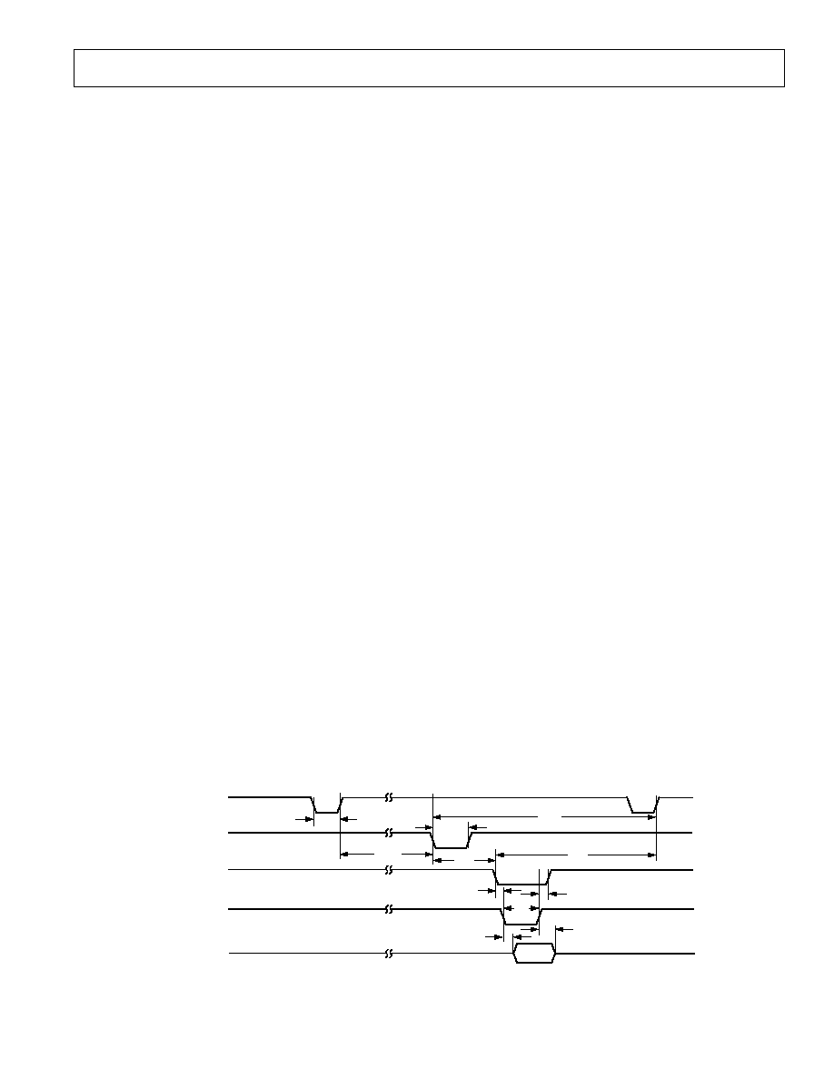
CONVST. CS and
RD going low accesses the 12-bit conversion result. In systems
where the part is interfaced to a gate array or ASIC, this
EOC
VALID
DATA
t
CONV
t
8
t
5
t
4
t
7
t
6
t
2
t
1
THREE-STATE
CONVST (I)
EOC (O)
CS (I)
RD (I)
DB0≠DB11 (O)
NOTE:
I = INPUT; O = OUTPUT
t
ACQ
t
3
t
9
THREE-STATE
Figure 2. Parallel Mode Timing Diagram
AD7892
≠10≠
REV. C
pulse can be applied to the
CS and RD inputs to latch data out
of the AD7892 and into the gate array or ASIC. This eliminates
the logic required in the gate array or ASIC to recognize the end
of conversion and generate the read signal for the AD7892. To
obtain optimum performance from the AD7892, it is not recom-
mended to tie
CS and RD permanently low as this keeps the
three-state active during conversion.
Serial Interface Mode
The AD7892 is configured for serial mode interfacing by tying
the MODE input low. It provides for a three-wire, serial link
between the AD7892 and industry-standard microprocessors,
microcontrollers and digital signal processors. SCLK and
RFS
of the AD7892 are inputs, and the AD7892's serial interface is
designed for direct interface to systems that provide a serial
clock input that is synchronized to the serial data output includ-
ing microcontrollers such as the 80C51, 87C51, 68HC11 and
68HC05 and most digital signal processors.
Figure 3 shows the timing diagram for reading from the AD7892
in the serial interface mode.
RFS goes low to access data from
the AD7892. The serial clock input does not have to be con-
tinuous. The serial data can be accessed in a number of bytes.
However,
RFS must remain low for the duration of the data
transfer operation. Sixteen bits of data are transmitted with four
leading zeros followed by the 12-bit conversion result starting
with the MSB. Serial data is clocked out of the device on the
rising edge of SCLK. Old data is guaranteed to be valid for 5 ns
after this edge. This is useful for high speed serial clocks where
the access time of the part would not allow sufficient set-up time
for the data to be accepted on the falling edge of the clock. In
this case, care must be taken that
RFS does not go just prior to
a rising edge of SCLK. For slower serial clocks data is valid on
the falling edge of SCLK. At the end of the read operation, the
SDATA line is three-stated by a rising edge on either the SCLK
or
RFS inputs, whichever occurs first. Serial data cannot be
read during conversion to avoid feedthrough problems from the
serial clock to the conversion process. For optimum perfor-
mance of the AD7892-3, a serial read should also be avoided
within 200 ns of the rising edge of
CONVST to avoid feedthrough
into the track/hold during its acquisition time. The serial read
should, therefore, occur between the end of conversion (
EOC
falling edge) and 200 ns prior to the next rising edge of
CONVST. For the AD7892-1 and AD7892-2, a serial read
should also be avoided within 400 ns of the rising edge of
CONVST. This limits the maximum achievable throughput
rate in serial mode (assuming 20 MHz serial clock) to 400 kSPS
for the AD7892-3 and 357 kSPS for the AD7892-1 and
AD7892-2.
Analog Input Section
The AD7892 is offered as three part types allowing for four
different analog input voltage ranges. The AD7892-1 handles
either
± 5 V or ± 10 V input voltage ranges. The AD7892-2
handles a 0 V to +2.5 V input voltage range while the AD7892-3
handles an input range of
±2.5 V.
AD7892-1
Figure 4 shows the analog input section for the AD7892-1. The
analog input range is pin-strappable (using V
IN2
) for either
±5 V
or
±10 V on the V
IN1
input. With V
IN2
connected to AGND, the
input range on V
IN1
is
±10 V, and the input resistance on V
IN1
is
15 k
nominal. With V
IN2
connected to V
IN1
, the input range on
V
IN1
is
±5 V, and the input resistance on V
IN1
is 8 k
nominal.
As a result, the V
IN1
and V
IN2
inputs should be driven from a
low impedance source. The resistor attenuator stage is followed
by the high input impedance stage of the track/hold amplifier.
This resistor attenuator stage allows the input voltage to go to
±17 V without damaging the AD7892-1.
+2.5
REFERENCE
REF OUT/
REF IN
V
IN1
V
IN2
AGND
TO HIGH
IMPEDANCE
SHA INPUT
TO ADC
REFERENCE
CIRCUITRY
2k
3.25k
13k
6.5k
13k
Figure 4. AD7892-1 Analog Input Structure
t
13
t
10
THREE-
STATE
RFS (I)
SCLK (I)
SDATA (O)
NOTE:
I = INPUT; O = OUTPUT
FOUR LEADING ZEROS
t
12
t
11
t
16
t
17
t
17A
t
14
DB11
DB10
DB0
t
15
Figure 3. Serial Mode Timing Diagram
AD7892
REV. C
≠11≠
The designed code transitions occur midway between successive
integer LSB values (i.e., 1/2 LSB, 3/2 LSBs, 5/2 LSBs). Output
coding is two's complement binary with 1 LSB = FSR/4096 =
20 V/4096 = 4.88 mV for the
±10 V range and 1 LSB = FSR/
4096 = 10 V/4096 = 2.44 mV for the
±5 V range. The ideal
input/output transfer function for the AD7892-1 is shown in
Table I.
AD7892-2
The analog input section for the AD7892-2 contains no biasing
resistors. The analog input looks directly into the track/hold
input stage. The analog input range on the V
IN1
input is 0 V to
+2.5 V. The V
IN2
input can be left unconnected but if it is
connected to a potential then that potential must be AGND.
The V
IN1
input connects directly to the input sampling capacitor
of the AD7892-2's track/hold. The value of this input sampling
capacitor is nominally 10 pF.
Once again, the designed code transitions occur midway be-
tween successive integer LSB values (i.e., 1/2 LSB, 3/2 LSBs,
5/2 LSBs). Output coding is straight (natural) binary with
1 LSB = FSR/4096 = 2.5 V/4096 = 0.61 mV. The ideal input/
output transfer function for the AD7892-2 is shown in Table II.
Table I. Ideal Input/Output Code Table for the AD7892-1
Digital Output
Analog Input
Code Transition
+FSR/2 ≠ 3/2 LSB
1, 2
(9.99268 or 4.99634)
3
011 . . . 110 to 011 . . . 111
+FSR/2 ≠ 5/2 LSBs (9.98779 or 4.99390)
011 . . . 101 to 011 . . . 110
+FSR/2 ≠ 7/2 LSBs (9.98291 or 4.99146)
011 . . . 100 to 011 . . . 101
AGND + 3/2 LSB (0.00732 or 0.00366)
000 . . . 001 to 000 . . . 010
AGND + 1/2 LSB (0.00244 or 0.00122)
000 . . . 000 to 000 . . . 001
AGND ≠ 1/2 LSB (≠0.00244 or ≠0.00122)
111 . . . 111 to 000 . . . 000
AGND ≠ 3/2 LSB (≠0.00732 or ≠0.00366)
111 . . . 110 to 111 . . . 111
≠FSR/2 + 5/2 LSB (≠9.98779 or ≠ 4.99390)
100 . . . 010 to 100 . . . 011
≠FSR/2 + 3/2 LSB (≠9.99268 or ≠ 4.99634)
100 . . . 001 to 100 . . . 010
≠FSR/2 + 1/2 LSB (≠9.99756 or ≠ 4.99878)
100 . . . 000 to 100 . . . 001
NOTES
1
FSR is full-scale range and REF IN = +2.5 V, is 20 V for the
±10 V range and 10 V
for the
±5 V range.
2
1 LSB = FSR/4096 = 4.88 mV (
±10 V range) and 2.44 mV (±5 V range) with REF
IN = +2.5 V.
3
± 10 V range or ±5 V range.
Table II. Ideal Input/Output Code Table for the AD7892-2
Digital Output
Analog Input
Code Transition
+FSR ≠ 3/2 LSB
1, 2
(2.499084 V)
111 . . . 110 to 111 . . . 111
+FSR ≠ 5/2 LSBs (2.498474 V)
111 . . . 110 to 111 . . . 110
+FSR ≠ 7/2 LSBs (2.497864 V)
111 . . . 100 to 111 . . . 101
AGND + 5/2 LSB (0.001526 V)
000 . . . 010 to 010 . . . 011
AGND + 3/2 LSB (0.00916 V)
000 . . . 001 to 001 . . . 010
AGND + 1/2 LSB (0.000305 V)
000 . . . 000 to 000 . . . 001
NOTES
1
FSR is full-scale range and is 2.5 V with REF IN = +2.5 V.
2
1 LSB = FSR/4096 = 0.61 mV with REF IN = +2.5 V.
AD7892-3
Figure 5 shows the analog input section for the AD7892-3. The
analog input range is
±2.5 V on the V
IN1
input. The V
IN2
input
can be left unconnected but if it is connected to a potential then
that potential must be AGND. The input resistance on the V
IN1
is 1.8 k
nominal. As a result, the V
IN1
input should be driven
from a low impedance source. The resistor attenuator stage is
followed by the high input impedance stage of the track/hold
amplifier. This resistor attenuator stage allows the input voltage
to go to
±7 V without damaging the AD7892-3.
The designed code transitions occur midway between succes-
sive integer LSB values (i.e., 1/2 LSB, 3/2 LSBs, 5/2 LSBs).
Output coding is two's complement binary with 1 LSB = FSR/
4096 = 5 V/4096 = 1.22 mV with REF IN = +2.5 V. The ideal
input/output transfer function for the AD7892-3 is shown in
Table III.
+2.5
REFERENCE
REF OUT/
REF IN
V
IN1
V
IN2
*
AGND
TO HIGH
IMPEDANCE
SHA INPUT
TO ADC
REFERENCE
CIRCUITRY
2k
3.25k
3.25k
* UNCONNECTED INTERNALLY ON THE AD7892-3
Figure 5. AD7892-3 Analog Input Structure
Table III. Ideal Input/Output Code Table for the AD7892-3
Digital Output
Analog Input
Code Transition
+FSR/2 ≠ 3/2 LSB
1, 2
(2.49817)
011 . . . 110 to 011 . . . 111
+FSR/2 ≠ 5/2 LSBs (2.49695)
011 . . . 110 to 011 . . . 110
+FSR/2 ≠ 7/2 LSBs (2.49573)
011 . . . 110 to 011 . . . 101
AGND + 3/2 LSB (0.00183)
000 . . . 001 to 000 . . . 010
AGND + 1/2 LSB (0.00061)
000 . . . 000 to 000 . . . 001
AGND ≠ 1/2 LSB (≠0.00061)
111 . . . 111 to 000 . . . 000
AGND ≠ 3/2 LSB (≠0.00183)
111 . . . 110 to 111 . . . 111
≠FSR/2 + 5/2 LSB (≠2.49695)
100 . . . 010 to 100 . . . 011
≠FSR/2 + 3/2 LSB (≠2.49817)
100 . . . 001 to 100 . . . 010
≠FSR/2 + 1/2 LSB (≠2.49939)
100 . . . 000 to 100 . . . 001
NOTES
1
FSR is full-scale range and is 5 V with REF IN = +2.5 V.
2
1 LSB = FSR/4096 = 1.22 mV with REF IN = +2.5 V.
AD7892
≠12≠
REV. C
MICROPROCESSOR INTERFACING
The AD7892 features both high speed parallel and serial inter-
faces, allowing considerable flexibility in interfacing to micro-
processor systems. To obtain optimum performance from the
part, data should not be read during conversion and this limits
the achievable throughput rate in serial mode to 400 kSPS for
the AD7892-3.
Figures 6, 7 and 9 show some typical interface circuits between
the AD7892 and popular DSP processors. Figure 8 shows an
interface between the part and a gate array or ASIC where data
is clocked into the ASIC by the AD7892 itself at the end of
conversion. In all cases, the
CONVST signal is generated from
an external timer to ensure equidistant sampling.
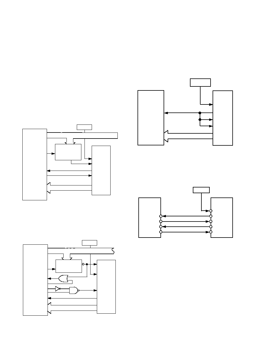
AD7892 to ADSP-2101 Interface
Figure 6 shows a parallel interface between the AD7892 and the
ADSP-2101 DSP processor.
CONVST starts conversion and at
the end of conversion the falling edge of the
EOC output pro-
vides an interrupt request to the ADSP-2101.
ADSP-2101
AD7892
ADDRESS DECODE
LOGIC
CONVST
CS
RD
DB11≠DB0
DATA BUS
ADDRESS BUS
DMA13≠DMA0
DMD15≠DMD0
IRQn
DMS
RD
EOC
EN
TIMER
Figure 6. AD7892 to ADSP-2101
AD7892 to TMS320C25 Interface
Figure 7 shows a parallel interface between the AD7892 and the
TMS320C25 DSP processor.
CONVST starts conversion and
at the end of conversion the falling edge of the
EOC output
provides an interrupt request to the TMS320C25.
TMS320C25
AD7892
ADDRESS DECODE
LOGIC
CONVST
CS
RD
DATA BUS
ADDRESS BUS
A15≠A0
D15≠D0
STRB
IS
INT
EOC
EN
TIMER
G2
READY
MSC
R/
W
DB11≠DB0
Figure 7. AD7892 to TMS320C25 Interface
EOC Pulse Provides
CS and RD
Figure 8 shows a parallel interface between the AD7892 and a
gate array or ASIC.
CONVST starts conversion and at the end
of conversion the falling edge of the
EOC output provides the
CS and RD pulse to latch data out of the AD7892 and into the
gate array/ASIC. This scheme allows for the fastest possible
throughput rate with the part as no time is lost in interrupt
service routines and as soon as data is available from the part it
is transferred out of it.
GATE
ARRAY/ASIC
AD7892
CONVST
CS
RD
DB11≠DB0
DATA BUS
DB11≠DB0
ENABLE
EOC
TIMER
Figure 8. AD7892 to Gate Array/ASIC Interface
AD7892 to DSP56000 Interface
Figure 9 shows a serial interface between the AD7892 and the
DSP56000 DSP processor.
CONVST starts conversion and at
the end of conversion the falling edge of the
EOC output pro-
vides an interrupt request to the DSP56000.
AD7892
CONVST
RFS
SDATA
EOC
TIMER
SCLK
DSP56000
SC1
SRD
IRQA
SCK
Figure 9. AD7892 to DSP56000 Interface

AD7892
REV. C
≠13≠
Grounding and Layout
The AD7892 has a single supply voltage pin, V
DD
, which sup-
plies both the analog and digital circuitry on the part. For opti-
mum performance from the part, it is recommended that this
+5 V is taken from the +5 V analog supply in the system. The
analog and digital grounds to the AD7892 are independent and
separately pinned out to minimize coupling between the analog
and digital sections of the device. The part exhibits good immu-
nity to noise on the supplies but care must still be taken with
regard to grounding and layout especially when using switching
mode supplies.
The printed circuit board which houses the AD7892 should be
designed such that the analog and digital sections are separated
and confined to certain areas of the board. This facilitates the
use of ground planes which can be separated easily. A minimum
etch technique is generally best for ground planes as it gives the
best shielding. Digital and analog ground planes should only be
joined in one place. If the AD7892 is the only device requiring
an AGND to DGND connection, then the ground planes
should be connected at the AGND and DGND pins of the
AD7892. If the AD7892 is in a system where multiple devices
require AGND to DGND connections, the connection should
still be made at one point only, a star ground point which
should be established as close as possible to the AD7892.
Avoid running digital lines under the device as these will couple
noise onto the die. The analog ground plane should be allowed
to run under the AD7892 to avoid noise coupling. The power
supply lines to the AD7892 should use as large a trace as pos-
sible to provide low impedance paths and reduce the effects of
glitches on the power supply line. Fast switching signals like
clocks should be shielded with digital ground to avoid radiating
noise to other sections of the board and clock signals should
never be run near the analog inputs. Avoid crossover of digital
and analog signals. Traces on opposite sides of the board should
run at right angles to each other. This will reduce the effects of
feedthrough through the board. A microstrip technique is by far
the best but is not always possible with a double-sided board. In
this technique, the component side of the board is dedicated to
ground planes while signals are placed on the solder side.
Good decoupling is important when using high resolution ADCs.
All analog supplies should be decoupled with 10
µF tantalum in
parallel with 0.1
µF capacitors to AGND. To achieve the best
from these decoupling components, they have to be placed as
close as possible to the device, ideally right up against the device.
All logic chips should be decoupled with 0.1
µF disc ceramic
capacitors to DGND. It is recommended that the system's
AV
DD
supply is used to supply the V
DD
for the AD7892. This
supply should have the recommended analog supply decoupling
capacitors between the V
DD
pin of the AD7892 and AGND and
the recommended digital supply decoupling capacitor between
the V
DD
pin of the AD7892 and DGND.
Evaluating the AD7892 Performance
The recommended layout for the AD7892 is outlined in the
evaluation board for the AD7892. The evaluation board package
includes a fully assembled and tested evaluation board, docu-
mentation and software for controlling the board from a PC
using the EVAL-CONTROL BOARD. The EVAL-CONTROL
BOARD can be used in conjunction with the AD7892 evalua-
tion board, as well as many other Analog Devices evaluation
boards ending in the CB designator. Using the EVAL-CONTROL
BOARD with the AD7892 evaluation board allows the user to
evaluate the ac and dc performance of the AD7892 on a PC.
The software provided with the evaluation board allows the user
to perform ac (Fast Fourier Transform) and dc (histogram of
codes) tests on the AD7892. The evaluation board can also
be used in a stand-alone fashion without the EVAL-CONTROL
BOARD but in this case, the user has to write their own software
to evaluate the part. There are two versions of the evaluation
board available, one for the AD7892-2 and one for the AD7892-3.
To order the AD7892-2 evaluation board, the order number is
EVAL-AD7892-2CB and to order the AD7892-3 evaluation
board, the order number is EVAL-AD7892-3CB.

AD7892
≠14≠
REV. C
OUTLINE DIMENSIONS
Dimensions shown in inches and (mm).
Plastic DIP (N-24)
24
1
12
13
0.260 ± 0.001
(6.61 ± 0.03)
PIN 1
1.228 (31.19)
1.226 (31.14)
0.11 (2.79)
0.09 (2.28)
SEATING
PLANE
0.02 (0.5)
0.016 (0.41)
0.130 (3.30)
0.128 (3.25)
0.07 (1.78)
0.05 (1.27)
0.32 (8.128)
0.30 (7.62)
0.011 (0.28)
0.009 (0.23)
15
0
Cerdip (Q-24)
24
1
12
13
0.310 (7.87)
0.220 (5.59)
PIN 1
0.005 (0.13) MIN
0.098 (2.49) MAX
SEATING
PLANE
0.023 (0.58)
0.014 (0.36)
0.200 (5.08)
MAX
1.280 (32.51) MAX
0.150
(3.81)
MIN
0.200 (5.08)
0.125 (3.18)
0.100 (2.54)
BSC
0.060 (1.52)
0.015 (0.38)
0.070 (1.78)
0.030 (0.76)
15∞
0∞
0.320 (8.13)
0.290 (7.37)
0.015 (0.38)
0.008 (0.20)
SOIC (R-24)
24
13
12
1
0.614 (15.6)
0.598 (15.2)
0.419 (10.65)
0.394 (10.00)
0.299 (7.60)
0.291(7.40)
PIN 1
SEATING
PLANE
0.012 (0.30)
0.004 (0.10)
0.019 (0.49)
0.014 (0.35)
0.1043 (2.65)
0.0926 (2.35)
0.050
(1.27)
BSC
0.013 (0.32)
0.009 (0.23)
0.050 (1.27)
0.015 (0.40)
8
0
0.0291 (0.74)
0.0098 (0.25)
45
C1933c≠2.5≠6/00 (rev. C) 01359
PRINTED IN U.S.A.