 | –≠–ª–µ–∫—Ç—Ä–æ–Ω–Ω—ã–π –∫–æ–º–ø–æ–Ω–µ–Ω—Ç: AD10201AB | –°–∫–∞—á–∞—Ç—å:  PDF PDF  ZIP ZIP |

REV. 0
Information furnished by Analog Devices is believed to be accurate and
reliable. However, no responsibility is assumed by Analog Devices for its
use, nor for any infringements of patents or other rights of third parties that
may result from its use. No license is granted by implication or otherwise
under any patent or patent rights of Analog Devices.
a
AD10201
One Technology Way, P.O. Box 9106, Norwood, MA 02062-9106, U.S.A.
Tel: 781/329-4700
www.analog.com
Fax: 781/326-8703
© Analog Devices, Inc., 2002
Dual-Channel, 12-Bit 105 MSPS
IF Sampling A/D Converter
FUNCTIONAL BLOCK DIAGRAM
D0B
(LSB)
D1B
D2B
D3B
D4B
D5B
D6B
D7B
D8B
D9B
D10B
D11B
(MSB)
D0A
(LSB)
D1A
D2A
D3A
D4A
D5A
D6A
D7A
D8A
D9A
D10A
D11A
(MSB)
ADC
50
A
IN
A2
T1A
ADC
50
A
IN
B2
T1B
AD10201
12
ENCODEA
ENCODEA
REF
REF_A_OUT
TIMING
ENCODEB
ENCODEB
REF
REF_B_OUT
OUTPUT
RESISTORS
T/H
T/H
TIMING
A
IN
A1
A
IN
B1
12
OUTPUT
RESISTORS
12
12
FEATURES
Two Independent 12-Bit, 105 MSPS ADCs
Channel-to-Channel Isolation, > 90 dB
AC-Coupled Signal Conditioning Included
Gain Flatness up to Nyquist, < 0.1 dB
Input VSWR 1.05:1 to Nyquist
80 dB Spurious-Free Dynamic Range
Two's Complement Output Format
3.3 V or 5 V CMOS-Compatible Output Levels
900 mW Per Channel
Single-Ended or Differential Input
250 MHz Input Bandwidth
APPLICATIONS
Wireless and Wired Broadband Communications
Base Stations and "Zero-IF" or Direct IF Sampling
Subsystems
Wireless Local Loop (WLL)
Local Multipoint Distribution Service (LMDS)
Radar and Satellite Subsystems
PRODUCT DESCRIPTION
The AD10201 offers two complete ADC channels with on-module
signal conditioning for improved dynamic performance. Each wide
dynamic range ADC has a transformer coupled front end optimized
for direct IF sampling. The AD10201 has on-chip track-and-hold
circuitry, and uses an innovative architecture to achieve 12-bit,
105 MSPS performance. The AD10201 uses innovative high
density circuit design to achieve exceptional performance while still
maintaining excellent isolation and providing for board area savings.
The AD10201 operates with 5.0 V supply for the analog-to-digital
conversion. Each channel is completely independent, allowing
operation with independent ENCODE and analog inputs. The
AD10201 is available as a 35 mm square 385-lead BGA package.
PRODUCT HIGHLIGHTS
1. Guaranteed sample rate of 105 MSPS
2. Input signal conditioning included with full-power bandwidth
to 250 MHz
3. Industry-leading IF sampling performance

REV. 0
≠2≠
AD10201≠SPECIFICATIONS
ELECTRICAL CHARACTERISTICS
1
Test
Parameter
Temp
Level
Min
Typ
Max
Unit
RESOLUTION
12
Bits
DC ACCURACY
Differential Nonlinearity
Full
IV
≠0.99
±0.5
+0.99
LSB
Integral Nonlinearity
Full
IV
±1.5
±0.1
+1.5
LSB
No Missing Codes
Full
IV
Guaranteed
Gain Error
2
25
∞C
I
≠9
±2
+9
% FS
Output Offset
25
∞C
I
≠8
±2
+8
LSB
Gain Tempco
Full
V
60
ppm/
∞C
Offset Tempco
Full
V
≠12
ppm/
∞C
ANALOG INPUT
Input Voltage Range
25
∞C
V
1.75
V p-p
Input Impedance
25
∞C
V
50
Input VSWR
3
Full
V
1.05:1
Ratio
Analog Input Bandwidth, High
Full
V
250
MHz
Analog Input Bandwidth, Low
Full
V
300
kHz
ANALOG REFERENCE
Output Voltage
25
∞C
V
2.5
V
Load Current
25
∞C
V
5
mA
Tempco
Full
V
50
ppm/
∞C
SWITCHING PERFORMANCE
4
Maximum Conversion Rate
Full
VI
105
MSPS
Minimum Conversion Rate
Full
IV
10
MSPS
Duty Cycle
Full
IV
45
50
55
%
Aperture Delay (t
A
)
25
∞C
V
2.0
ns
Aperture Uncertainty (Jitter)
25
∞C
V
0.25
ps rms
Output Valid Time (t
V
)
5
Full
IV
3.0
6.3
ns
Output Propagation Delay (t
PD
)
5
Full
IV
6.5
9.0
ns
Output Rise Time (t
R
)
25
∞C
V
3.5
ns
Output Fall Time (t
F
)
25
∞C
V
3.3
ns
DIGITAL INPUTS
ENCODE Input Common-Mode
Full
IV
1.2
1.6
2.0
V
Differential Input (ENC,
ENC)
Full
IV
0.4
5.0
V
Logic "1" Voltage
Full
IV
2.0
V
Logic "0" Voltage
Full
IV
0.8
V
Input Resistance
Full
IV
3
5
8.0
k
Input Capacitance
25
∞C
V
4.5
pF
DIGITAL OUTPUTS
Logic "1" Voltage
5
Full
IV
3.1
3.3
V
Logic "0" Voltage
5
Full
IV
0
0.2
V
Output Coding
Two's Complement
POWER SUPPLY
6
Power Dissipation
7
Full
VI
1800
2200
mW
Power Supply Rejection Ratio
Full
IV
≠5.0
±0.5
+5.0
mV/V
Total I (DV
DD
) Current
Full
VI
32
40
mA
Total I (AV
CC
) Current
Full
VI
340
410
mA
(V
DD
= 3.3 V, V
CC
= 5.0 V; ENCODE = 105 MSPS, unless otherwise noted.)
REV. 0
≠3≠
AD10201
Test
Parameter
Temp
Level
Min
Typ
Max
Unit
DYNAMIC PERFORMANCE
Signal-to-Noise Ratio (SNR)
8
(Without Harmonics)
f
IN
= 10 MHz
25
∞C
I
66
68
dBFS
f
IN
= 41 MHz
25
∞C
V
67
dBFS
f
IN
= 71 MHz
25
∞C
I
63.5
66.5
dBFS
f
IN
= 121 MHz
25
∞C
V
63
dBFS
Signal-to-Noise Ratio (SINAD)
9
(With Harmonics)
f
IN
= 10 MHz
25
∞C
I
65.5
67.5
dBFS
f
IN
= 41 MHz
25
∞C
V
67.2
dBFS
f
IN
= 71 MHz
25
∞C
I
63
65
dBFS
f
IN
= 121 MHz
25
∞C
V
59
dBFS
Spurious-Free Dynamic Range
10
f
IN
= 10 MHz
25
∞C
I
75.5
81
dBFS
f
IN
= 41 MHz
25
∞C
V
76
dBFS
f
IN
= 71 MHz
25
∞C
I
71
74
dBFS
f
IN
= 121 MHz
25
∞C
V
63
dBFS
Two-Tone Intermodulation
Distortion
11
(IMD)
f
IN
= 10 MHz; f
IN
= 12 MHz
25
∞C
V
81
dBc
f
IN
= 71 MHz; f
IN
= 72 MHz
25
∞C
V
66
dBc
f
IN
= 121 MHz; f
IN
= 122 MHz
25
∞C
V
61
dBc
Channel-to-Channel Isolation
12
f
IN
= 121 MHz
Full
IV
90
dBc
NOTES
1
All specifications tested by driving ENCODE and
ENCODE differentially, with the analog input applied to A
IN
X1 and A
IN
X2 tied to ground.
2
Gain error measured at 10.3 MHz.
3
Input VSWR, see TPC 12.
4
See Figure 1, Timing Diagram.
5
t
V
and t
PD
are measured from the transition points of the ENCODE input to the 50%/50% levels of the digital outputs swing. The digital output load during test is
not to exceed an ac load of 10 pF or a dc current of
±40 A.
6
Supply voltages should remain stable within
±5% for normal operation.
7
Power dissipation measures with encode at rated speed.
8
Analog input signal power at ≠1 dBFS; signal-to-noise (SNR) is the ratio of signal level to total noise (first six harmonics removed).
ENCODE = 105 MSPS. SNR is reported in dBFS, related back to converter full scale.
9
Analog input signal power at ≠1 dBFS; signal-to-noise and distortion (SINAD) is the ratio of signal level to total noise + harmonics. ENCODE = 105 MSPS.
SINAD is reported in dBFS, related back to converter full scale.
10
Analog input signal equals ≠1 dBFS; SFDR is ratio of converter full scale to worst spur.
11
Both input tones at ≠7 dBFS; two-tone intermodulation distortion (IMD) rejection is the ratio of either tone to the worst third order intermod product.
12
Channel-to-channel isolation tested with A channel/50
terminated (A
IN
A2 grounded) and a full-scale signal applied to B channel (A
IN
B2).
Specifications subject to change without notice.

REV. 0
AD10201
≠4≠
CAUTION
ESD (electrostatic discharge) sensitive device. Electrostatic charges as high as 4000 V readily
accumulate on the human body and test equipment and can discharge without detection. Although
the AD10201 features proprietary ESD protection circuitry, permanent damage may occur on
devices subjected to high-energy electrostatic discharges. Therefore, proper ESD precautions are
recommended to avoid performance degradation or loss of functionality.
WARNING!
ESD SENSITIVE DEVICE
ABSOLUTE MAXIMUM RATINGS
*
V
DD
. . . . . . . . . . . . . . . . . . . . . . . . . . . . . . . . . . . . . . . . . . 6 V
V
CC
. . . . . . . . . . . . . . . . . . . . . . . . . . . . . . . . . . . . . . . . . . 6 V
Analog Inputs . . . . . . . . . . . . . . . . . . . . . . 5 V p-p (18 dBm)
Digital Inputs . . . . . . . . . . . . . . . . . . . . ≠0.5 V to V
DD
+0.5 V
Digital Output Current . . . . . . . . . . . . . . . . . . . . . . . . 20 mA
Operating Temperature (Ambient) . . . . . . . ≠55
∞C to +125∞C
Storage Temperature (Ambient) . . . . . . . . . ≠65
∞C to +150∞C
Maximum Junction Temperature . . . . . . . . . . . . . . . . . 150
∞C
* Stresses above those listed under Absolute Maximum Ratings may cause permanent
damage to the device. This is a stress rating only; functional operation of the device
at these or any other conditions outside of those indicated in the operation sections
of this specification is not implied. Exposure to absolute maximum ratings for
extended periods may affect device reliability.
THERMAL CHARACTERISTICS
385-Lead BGA Package:
The typical
JA
of the module as determined by an IR scan is
25.33
∞C/W.
t
PD
AIN
ENCODE
ENCODE
D11 D0
SAMPLE N 1
SAMPLE N
SAMPLE N 10
SAMPLE N 11
SAMPLE N 9
SAMPLE N 1
1/f
S
DATA N 11
DATA N 10
N 9
DATA N 1
DATA N
DATA N 1
t
V
N 2
Figure 1. Timing Diagram
ORDERING GUIDE
Model
Temperature Range
Package Description
Package Option
AD10201AB
≠25
∞C to +85∞C (Ambient)
385-Lead BGA (35 mm 35 mm)
B-385
AD10201/PCB
+25
∞C
Evaluation Board with AD10201AB
EXPLANATION OF TEST LEVELS
Test Level
I
100% production tested
II
100% production tested at 25
∞C and sample tested at specific
temperatures
III Sample tested only
IV Parameter is guaranteed by design and characterization
testing
V
Parameter is a typical value only
VI 100% production tested at 25
∞C; guaranteed by design and
characterization testing for industrial temperature range
Table I. Output Coding (V
REF
= 2.5 V) (Two's Complement)
Code
A
IN
(V)
Digital Output
+2047
+0.875
0111 1111 1111
∑
∑
∑
∑
∑
∑
0
0
0000 0000 0000
≠1
≠0.000427
1111 1111 1111
∑
∑
∑
∑
∑
∑
≠2048
≠0.875
1000 0000 0000
REV. 0
AD10201
≠5≠
PIN CONFIGURATION
35 mm square
BOTTOM VIEW
A
B
C
D
E
F
G
H
J
K
L
M
N
P
R
T
U
V
W
Y
AA
AB
AC
AD
AE
24
22
20
18
16
14
12
10
8
6
4
2
25
23
21
19
17
15
13
11
9
7
5
3
1
PIN FUNCTION DESCRIPTIONS
Mnemonic
Function
AGNDA
A Channel Analog Ground. A and B grounds should be connected as close to the device as possible
REF_A_OUT
A Channel Internal Voltage Reference
NC
No connection
A
IN
A1
Analog Input for A side ADC ( input)
A
IN
A2
Analog Input for A side ADC (+ input)
AV
CC
A
Analog Positive Supply Voltage (nominally 5.0 V)
DGNDA
A Channel Digital Ground
D11A≠D0A
Digital Outputs for ADC A. D0 (LSB)
ENCODEA
Complement of ENCODE
ENCODEA
Data conversion initiated on the rising edge of ENCODE input
DV
CC
A
Digital Positive Supply Voltage (nominally 3.3 V)
DGNDB
B Channel Digital Ground
D11B≠D0B
Digital Outputs for ADC B. D0 (LSB)
AGNDB
B Channel Analog Ground. A and B grounds should be connected as close to the device as possible.
DV
CC
B
Digital Positive Supply Voltage (nominally 3.3 V)
ENCODEB
Complement of ENCODE
ENCODEB
Data conversion initiated on rising edge of ENCODE input
REF_B_OUT
B Channel Internal Voltage Reference
A
IN
B1
Analog Input for B side ADC ( input)
A
IN
B2
Analog Input for B side ADC (+ input)
AV
CC
B
Analog Positive Supply Voltage (nominally 5.0 V)

REV. 0
AD10201
≠6≠
A1
AGNDA
A2
AGNDA
A3
AGNDA
A4
AGNDA
A5
AGNDA
A6
AGNDA
A7
DNC
A8
DNC
A9
AGNDA
A10
AV
CC
A
A11
REF_A_OUT
A12
AGNDA
A13
DNC
A14
AGNDB
A15
AGNDB
A16
AV
CC
B
A17
AGNDB
A18
AV
CC
B
A19
DNC
A20
DNC
A21
AGNDB
A22
AGNDB
A23
AGNDB
A24
AGNDB
A25
AGNDB
B1
AGNDA
B2
AGNDA
B3
AGNDA
B4
AGNDA
B5
AGNDA
B6
AGNDA
B7
DNC
B8
DNC
B9
AGNDA
B10
AV
CC
A
B11
REF_A_OUT
B12
AGNDA
B13
DNC
B14
AGNDB
B15
AGNDB
B16
AV
CC
B
B17
AGNDB
B18
AV
CC
B
B19
DNC
B20
DNC
B21
AGNDB
B22
AGNDB
B23
AGNDB
B24
AGNDB
B25
AGNDB
C1
AGNDA
C2
AGNDA
C3
AGNDA
C4
AGNDA
C5
AGNDA
C6
AGNDA
C7
DNC
C8
DNC
C9
AGNDA
C10
AV
CC
A
C11
REF_A_OUT
C12
AGNDA
C13
DNC
C14
AGNDB
C15
AGNDB
C16
AV
CC
B
C17
AGNDB
C18
AV
CC
B
C19
DNC
C20
DNC
C21
AGNDB
C22
AGNDB
C23
AGNDB
C24
AGNDB
C25
AGNDB
D1
AGNDA
D2
AGNDA
D3
AGNDA
D4
AGNDA
D5
AGNDA
D6
AGNDA
D7
A
IN
A2
D8
A
IN
A1
D9
AGNDA
D10
AV
CC
A
D11
REF_A_OUT
D12
AGNDA
D13
DNC
D14
AGNDB
D15
AGNDB
D16
AV
CC
B
D17
AGNDB
D18
AV
CC
B
D19
A
IN
B2
D20
A
IN
B1
D21
AGNDB
D22
AGNDB
D23
AGNDB
D24
AGNDB
D25
AGNDB
E1
AGNDA
E2
AGNDA
E3
AGNDA
E4
AGNDA
E22
AGNDB
E23
AGNDB
E24
AGNDB
E25
AGNDB
F1
AGNDA
F2
AGNDA
F3
AGNDA
F4
AGNDA
F22
AGNDB
F23
AGNDB
F24
AGNDB
F25
AGNDB
G1
AGNDA
G2
AGNDA
G3
AGNDA
G4
AGNDA
G22
AGNDB
G23
AGNDB
G24
AGNDB
G25
AGNDB
H1
AGNDA
H2
AGNDA
H3
AGNDA
H4
AGNDA
H22
AGNDB
H23
AGNDB
H24
AGNDB
H25
AGNDB
J1
AV
CC
A
J2
AV
CC
A
J3
AV
CC
A
J4
AV
CC
A
J22
REF_B_OUT
J23
REF_B_OUT
J24
REF_B_OUT
J25
REF_B_OUT
K1
AGNDA
K2
AGNDA
K3
AGNDA
K4
AGNDA
K10
AV
CC
A
K11
AGNDA
K12
AGNDA
K13
DNC
K14
AGNDB
K15
AGNDB
K16
AV
CC
B
K22
AGNDB
K23
AGNDB
K24
AGNDB
K25
AGNDB
L1
AGNDA
L2
AGNDA
L3
AGNDA
L4
AGNDA
L10
DNC
L11
AGNDA
L12
AGNDA
L13
DNC
L14
AGNDB
L15
AGNDB
L16
DNC
L22
ENCBB
L23
ENCBB
L24
ENCBB
L25
ENCBB
M1
ENCAB
M2
ENCAB
M3
ENCAB
M4
ENCAB
M10
AGNDA
M11
AGNDA
M12
AGNDA
M13
DNC
M14
AGNDB
M15
AGNDB
M16
AGNDB
M22
ENCB
M23
ENCB
M24
ENCB
M25
ENCB
N1
ENCA
N2
ENCA
N3
ENCA
N4
ENCA
N10
AGNDA
N11
AGNDA
N12
AGNDA
N13
DNC
N14
AGNDB
N15
AGNDB
N16
AGNDB
N22
AGNDB
N23
AGNDB
N24
AGNDB
N25
AGNDB
P1
AGNDA
P2
AGNDA
P3
AGNDA
P4
AGNDA
P10
AGNDA
P11
AGNDA
P12
AGNDA
P13
DNC
P14
AGNDB
P15
AGNDB
P16
AGNDB
P22
DV
CC
B
P23
DV
CC
B
P24
DV
CC
B
P25
DV
CC
B
P25
DV
CC
B
R1
DV
CC
A
R2
DV
CC
A
R3
DV
CC
A
R4
DV
CC
A
R10
AGNDA
R11
AGNDA
R12
AGNDA
R13
DNC
R14
AGNDB
R15
AGNDB
R16
AGNDB
R22
DB0
R23
DB0
R24
DB0
R25
DB0
T1
DA11
T2
DA11
T3
DA11
T4
DA11
T10
AV
CC
A
T11
AGNDA
T12
AGNDA
T13
DNC
T14
AV
CC
B
T15
AGNDB
T16
AGNDB
T22
DB1
T23
DB1
T24
DB1
T25
DB1
U1
DA10
U2
DA10
U3
DA10
U4
DA10
U22
DB2
U23
DB2
U24
DB2
U25
DB2
V1
DA9
V2
DA9
V3
DA9
V4
DA9
V22
DB3
V23
DB3
V24
DB3
V25
DB3
W1
DA8
W2
DA8
W3
DA8
W4
DA8
W22
DB4
W23
DB4
W24
DB4
W25
DB4
Y1
DA7
Y2
DA7
Y3
DA7
Y4
DA7
Y22
DB5
Y23
DB5
Y24
DB5
Y25
DB5
AA1
DGNDA
AA2
DGNDA
AA3
DGNDA
AA4
DGNDA
AA22 DGNDB
AA23 DGNDB
AA24 DGNDB
AA25 DGNDB
AB1
OVRA
AB2
OVRA
AB3
OVRA
AB4
OVRA
AB5
DGNDA
AB6
DA6
AB7
DA5
AB8
DA4
AB9
DA3
AB10 DA2
AB11 DA1
AB12 DA0
AB13 DGNDA
AB14 DGNDB
AB15 DB11
AB16 DB10
AB17 DB9
AB18 DB8
AB19 DB7
AB20 DB6
AB21 DGNDB
AB22 OVRB
AB23 OVRB
AB24 OVRB
AB25 OVRB
AC1
DGNDA
AC2
DGNDA
AC3
DGNDA
AC4
DGNDA
AC5
DGNDA
AC6
DA6
AC7
DA5
AC8
DA4
AC9
DA3
AC10 DA2
AC11 DA1
AC12 DA0
AC13 DGNDA
AC14 DGNDB
AC15 DB11
AC16 DB10
AC17 DB9
AC18 DB8
AC19 DB7
AC20 DB6
AC21 DGNDB
AC22 DGNDB
AC23 DGNDB
AC24 DGNDB
AC25 DGNDB
AD1
DGNDA
AD2
DGNDA
AD3
DGNDA
AD4
DGNDA
AD5
DGNDA
AD6
DA6
AD7
DA5
AD8
DA4
AD9
DA3
AD10 DA2
AD11 DA1
AD12 DA0
AD13 DGNDA
AD14 DGNDB
AD15 DB11
AD16 DB10
AD17 DB9
AD18 DB8
AD19 DB7
AD20 DB6
AD21 DGNDB
AD22 DGNDB
AD23 DGNDB
AD24 DGNDB
AD25 DGNDB
AE1
DGNDA
AE2
DGNDA
AE3
DGNDA
AE4
DGNDA
AE5
DGNDA
AE6
DA6
AE7
DA5
AE8
DA4
AE9
DA3
AE10 DA2
AE11 DA1
AE12 DA0
AE13 DGNDA
AE14 DGNDB
AE15 DB11
AE16 DB10
AE17 DB9
AE18 DB8
AE19 DB7
AE20 DB6
AE21 DGNDB
AE22 DGNDB
AE23 DGNDB
AE24 DGNDB
AE25 DGNDB
385-LEAD BGA PINOUT
Ball
Signal
Ball
Signal
Ball
Signal
Ball
Signal
Ball
Signal
Ball
Signal
No.
Name
No.
Name
No.
Name
No.
Name
No.
Name
No.
Name

REV. 0
AD10201
≠7≠
385-LEAD BGA PINOUT (Top View, PCB Footprint)
DNC = DO NOT CONNECT
1
AGNDA
AGNDA
AGNDA
AGNDA
AGNDA
AGNDA
AGNDA
AGNDA
AGNDA
AGNDA
AGNDA
DGNDA
OVRA
DGNDA
DGNDA
DGNDA
DGNDA
DGNDA
DGNDA
DGNDA
DA6
DA6
DA6
DA6
A
B
C
D
E
F
G
H
J
K
L
M
N
P
R
T
U
V
W
Y
AA
AB
AC
AD
AE
DGNDA
OVRA
DGNDA
DGNDA
DGNDA
DGNDA
OVRA
DGNDA
DGNDA
DGNDA
DGNDA
OVRA
DGNDA
DGNDA
DGNDA
DGNDA
DGNDA
DGNDA
DGNDA
DGNDB
DGNDB
DGNDB
DGNDB
DB11
DB11
DB11
DB11
DB10
DB10
DB10
DB10
DB9
DB9
DB9
DB9
DB8
DB8
DB8
DB8
DB7
DB7
DB7
DB7
DB6
DB6
DB6
DB6
DGNDB
DGNDB
DGNDB
DGNDB
OVRB
DGNDB
DGNDB
DGNDB
AGNDA
AGNDA
AGNDA
AGNDA
AGNDA
AGNDA
AGNDA
DNC
DNC
DNC
DNC
DNC
DNC
DNC
AGNDB
AGNDB
AGNDB
AGNDB
AGNDB
AGNDB
AV
CC
B
ENCAB
ENCA
AGNDA
DV
CC
A
DA11
DA10
DA9
DA8
DA7
2
AGNDA
AGNDA
AGNDA
AGNDA
AGNDA
AGNDA
AGNDA
AGNDA
AGNDA
AGNDA
AGNDA
3
AGNDA
AGNDA
AGNDA
AGNDA
AGNDA
AGNDA
AGNDA
AGNDA
AGNDA
AGNDA
AGNDA
4
AGNDA
AGNDA
AGNDA
AGNDA
AGNDA
AGNDA
AGNDA
AGNDA
AGNDA
AGNDA
AGNDA
5
AGNDA
AGNDA
AGNDA
AGNDA
6
AGNDA
AGNDA
AGNDA
AGNDA
7
DNC
DNC
DNC
AINA2
8
DNC
DNC
DNC
AINA1
9
AGNDA
AGNDA
AGNDA
AGNDA
12
AGNDA
AGNDA
AGNDA
AGNDA
10
AV
CC
A
AV
CC
A
AV
CC
A
AV
CC
A
11
REF_A_OUT
REF_A_OUT
REF_A_OUT
REF_A_OUT
13
DNC
DNC
DNC
DNC
14
AGNDB
AGNDB
AGNDB
AGNCB
15
AGNDB
AGNDB
AGNDB
AGNCB
16
AV
CC
B
AV
CC
B
AV
CC
B
AV
CC
B
17
AGNDB
AGNDB
AGNDB
AGNCB
18
AV
CC
B
AV
CC
B
AV
CC
B
AV
CC
B
19
DNC
DNC
DNC
A
IN
B2
21
AGNDB
AGNDB
AGNDB
AGNDB
20
DNC
DNC
DNC
A
IN
B1
22
AGNDB
AGNDB
AGNDB
AGNDB
AGNDB
AGNDB
AGNDB
AGNDB
REF_B_OUT
AGNDB
ENCBB
ENCB
AGNDB
DV
CC
B
DB0
DB1
DB2
DB3
DB4
DB5
DGNDB
23
AGNDB
AGNDB
AGNDB
AGNDB
AGNDB
AGNDB
AGNDB
AGNDB
24
AGNDB
AGNDB
AGNDB
AGNDB
AGNDB
AGNDB
AGNDB
AGNDB
25
AGNDB
AGNDB
AGNDB
AGNDB
AGNDB
AGNDB
AGNDB
AGNDB
OVRB
DGNDB
DGNDB
DGNDB
OVRB
DGNDB
DGNDB
DGNDB
OVRB
DGNDB
DGNDB
DGNDB
DB0
DB1
DB2
DB3
DB4
DB5
DGNDB
DB0
DB1
DB2
DB3
DB4
DB5
DGNDB
DB0
DB1
DB2
DB3
DB4
DB5
DGNDB
ENCAB
ENCA
AGNDA
DV
CC
A
DA11
DA10
DA9
DA8
DA7
ENCAB
ENCA
AGNDA
DV
CC
A
DA11
DA10
DA9
DA8
DA7
ENCAB
ENCA
AGNDA
DV
CC
A
DA11
DA10
DA9
DA8
DA7
AV
CC
B
DNC
AGNDB
AGNDB
AGNDB
AGNDB
AGNDB
AGNDB
AGNDB
AGNDB
AGNDB
AGNDB
AGNDB
AGNDB
AGNDA
AGNDA
AGNDA
AGNDA
AGNDA
AGNDA
AGNDA
AV
CC
A
DNC
AGNDA
AGNDA
AGNDA
AGNDA
AV
CC
A
DA5
DA5
DA5
DA5
DA4
DA4
DA4
DA4
DA3
DA3
DA3
DA3
DA2
DA2
DA2
DA2
DA1
DA1
DA1
DA1
DA0
DA0
DA0
DA0
REF_B_OUT
AGNDB
ENCBB
ENCB
AGNDB
DV
CC
B
REF_B_OUT
AGNDB
ENCBB
ENCB
AGNDB
DV
CC
B
REF_B_OUT
AGNDB
ENCBB
ENCB
AGNDB
DV
CC
B

REV. 0
AD10201
≠8≠
FREQUENCY ≠ MHz
0
130
dB
20
80
100
110
120
40
60
0
10
30
90
50
70
5
10
15
20
25
30
35
40
45
50
ENCODE = 105MSPS
A
IN
= 10MHz (≠1dBFS)
SNR = 67.65dBFS
SFDR = 88.14dBFS
TPC 1. Single Tone @ 10 MHz
FREQUENCY ≠ MHz
0
130
dB
20
80
100
110
120
40
60
0
10
30
90
50
70
5
10
15
20
25
30
35
40
45
50
ENCODE = 105MSPS
A
IN
= 49MHz (≠1dBFS)
SNR = 66.97dBFS
SFDR = 82.66dBFS
TPC 2. Single Tone @ 49 MHz
FREQUENCY ≠ MHz
0
130
dB
20
80
100
110
120
40
60
0
10
30
90
50
70
5
10
15
20
25
30
35
40
45
50
ENCODE = 105MSPS
A
IN
= 71MHz (≠1dBFS)
SNR = 66.1dBFS
SFDR = 81.3dBFS
TPC 3. Single Tone @ 71 MHz
FREQUENCY ≠ MHz
0
130
dB
20
80
100
110
120
40
60
0
10
30
90
50
70
5
10
15
20
25
30
35
40
45
50
ENCODE = 105MSPS
A
IN
= 121MHz (≠1dBFS)
SNR = 64.4dBFS
SFDR = 65.4dBFS
TPC 4. Single Tone @ 121 MHz
FREQUENCY ≠ MHz
0
130
dB
20
80
100
110
120
40
60
0
10
30
90
50
70
5
10
15
20
25
30
35
40
45
50
ENCODE = 105MSPS
A
IN
= 10.3MHz AND 12MHz
SFDR = 87.82dBFS
TPC 5. Two Tone @ 10/12 MHz
FREQUENCY ≠ MHz
0
130
dB
20
80
100
110
120
40
60
0
10
30
90
50
70
5
10
15
20
25
30
35
40
45
50
ENCODE = 105 MSPS
A
IN
= 71 AND 72 MHz
SFDR = 83.03dBFS
F
2
∑
F
1
2
F
1
∑
F
2
2
F
1
∑
F
2
2
F
2
∑
F
1
F
1
+
F
2
2
F
2
∑
F
1
TPC 6. Two Tone @ 71/72 MHz
≠ Typical Performance Characteristics

REV. 0
AD10201
≠9≠
FREQUENCY ≠ MHz
0
130
dB
20
80
100
110
120
40
60
0
10
30
90
50
70
5
10
15
20
25
30
35
40
45
50
ENCODE = 105MSPS
A
IN
= 121MHz AND 122MHz
SFDR = 69.05dBFS
TPC 7. Two Tone @ 121/122 MHz
GAIN ≠ dB
6
2
10
4
FREQUENCY ≠ MHz
3
5
100
1000
1
1
0
TPC 8. Gain Flatness*
3.0
1.0
LSB
1.5
0.5
0.0
0.5
2.5
0
1.0
2.0
512
1024
1536
2048
2560
3072
3584
4096
ENCODE = 105MSPS
DNL MIN = 0.244
DNL MAX = 0.306
OUTPUT CODES
TPC 9. Differential Nonlinearity
*Gain flatness measurement is performed by
applying a constant voltage at the device input.
3.0
3.0
LSB
0.0
0
1.0
2.0
512
1024
1536
2048
2560
3072
3584
4096
2.0
1.0
ENCODE = 105MSPS
INL MIN = 0.586
INL MAX = 0.472
OUTPUT CODES
TPC 10. Integral Nonlinearity
1MHz = 1.007
10MHz = 1.030
50MHz = 1.028
100MHz = 1.042
140MHz = 1.095
160MHz = 1.134
200MHz = 1.254
TPC 11. Input Impedance S11
FREQUENCY ≠ MHz
0.1
1
GAIN ≠ dB
10
1
2
3
4
5
6
7
8
9
10
0
100
1000
10MHz = 51.45 j 0.09
50MHz = 50.34 j 1.21
100MHz = 47.91 j 0.05
150MHz = 46.57 j 4.13
200MHz = 48.92 j 10.0
TPC 12. Voltage Standing Wave Ratio (VSWR)
REV. 0
AD10201
≠10≠
V
CC
17k
8k
100
100
17k
8k
ENCODE
ENCODE
Test Circuit 1. Equivalent ENCODE Input
V
CC
100
DIGITAL
OUTPUT
Test Circuit 2. Equivalent Digital Output
Q1
NPN
V
REF
OUTPUT
V
CC
V
CC
Test Circuit 3. Equivalent Voltage Reference Output
V
CC
A
IN
2
7k
50
7k
5k
5k
A
IN
1
Test Circuit 4. Equivalent Analog Input
DEFINITION OF TERMS
Analog Bandwidth
The analog input frequency at which the spectral power of the
fundamental frequency (as determined by the FFT analysis) is
reduced by 3 dB.
Aperture Delay
The delay between the 50% point on the rising edge of the ENCODE
command and the instant at which the analog input is sampled.
Aperture Uncertainty (Jitter)
The sample-to-sample variation in aperture delay.
Differential Nonlinearity
The deviation of any code from an ideal 1 LSB step.
ENCODE Pulsewidth/Duty Cycle
Pulsewidth high is the minimum amount of time that the
ENCODE pulse should be left in logic "1" state to achieve rated
performance; pulsewidth low is the minimum time ENCODE
pulse should be left in low state. At a given clock rate, these specs
define an acceptable ENCODE duty cycle.
Harmonic Distortion
The ratio of the rms signal amplitude to the rms value of the
worst harmonic component.
Integral Nonlinearity
The deviation of the transfer function from a reference line measured
in fractions of 1 LSB using a "best straight line" determined by
a least square curve fit.
Minimum Conversion Rate
The ENCODE rate at which the SNR of the lowest analog signal
frequency drops by no more than 3 dB below the guaranteed limit.
Maximum Conversion Rate
The ENCODE rate at which parametric testing is performed.
Output Propagation Delay
The delay between the 50% point of the rising edge of ENCODE
command and the time when all output data bits are within valid
logic levels.
Power Supply Rejection Ratio
The ratio of a change in output offset voltage to a change in
power supply voltage.
Signal-to-Noise-and-Distortion (SINAD)
The ratio of the rms signal amplitude (set at 1 dB below full-scale)
to the rms value of the sum of all other spectral components,
excluding the first six harmonics and dc. [May be reported in dBc
(i.e., degrades as signal levels are lowered) or in dBFS (always
related back to converter full-scale).]
Signal-to-Noise Ratio (without Harmonics)
The ratio of the rms signal amplitude (set at 1 dB below full-scale)
to the rms value of the sum of all other spectral components,
excluding the first six harmonics and dc. [May be reported in
dBc (i.e., degrades as signal levels are lowered) or in dBFS (always
related back to converter full-scale).]
Spurious-Free Dynamic Range
The ratio of the rms signal amplitude to the rms value of the peak
spurious spectral component. The peak spurious component may
or may not be a harmonic. [May be reported in dBc (i.e., degrades
as signal levels is lowered) or in dBFS (always related back to
converter full-scale).]
Two-Tone Intermodulation Distortion Rejection
The ratio of the rms value of either input tone to the rms value
of the worst third order intermodulation product; reported in dBc.
Voltage Standing Wave Ratio (VSWR)
The ratio of the amplitude of the electric field at a voltage maximum
to that at an adjacent voltage minimum.
≠ Equivalent Circuits

REV. 0
AD10201
≠11≠
Often, the cleanest clock source is a crystal oscillator producing
a pure sine wave. In this configuration, or with any roughly sym-
metrical clock input, the input can be ac-coupled and biased to a
reference voltage that also provides the ENCODE. This ensures
that the reference voltage is centered on the encode signal.
Digital Outputs
The digital outputs are 3.3 V (2.7 V to 3.6 V) TTL/CMOS-
compatible for lower power consumption.
Analog Input
The analog input is a single-ended ac-coupled high performance
1:1 transformer with an input impedance of 50
to 250 MHz.
The nominal full-scale input is 1.75 V p-p.
Special care was taken in the design of the analog input section
of the AD10201 to prevent damage and corruption of data when
the input is overdriven.
Voltage Reference
A stable and accurate 2.5 V voltage reference is designed into the
AD10201 (V
REFOUT
). An external voltage reference is not required.
Timing
The AD10201 provides latched data outputs, with 10 pipeline
delays. Data outputs are available one propagation delay (t
PD
) after
the rising edge of the ENCODE command (see Figure 1). The
length of the output data lines and loads placed on them should
be minimized to reduce transients within the AD10201; these
transients can detract from the converter's dynamic performance.
The minimum guaranteed conversion rate of the AD10201 is
10 MSPS. At internal clock rates below 10 MSPS dynamic perfor-
mance may degrade. Therefore, input clock rates below 10 MHz
should be avoided.
GROUNDING AND DECOUPLING
Analog and Digital Grounding
Proper grounding is essential in any high speed, high resolution
system. Multilayer printed circuit boards (PCBs) are recommended
to provide optimal grounding and power schemes. The use of
ground and power planes offers distinct advantages:
1. The minimization of the loop area encompassed by a signal
and its return path.
2. The minimization of the impedance associated with ground
and power paths.
3. The inherent distributed capacitor formed by the powerplane,
PCB insulation, and ground plane.
These characteristics result in both a reduction of electromagnetic
interference (EMI) and an overall improvement in performance.
It is important to design a layout that prevents noise from coupling
to the input signal. Digital signals should not be run in parallel
with input signal traces and should be routed away from the input
circuitry. The PCB should have a ground plane covering all unused
portions of the component side of the board to provide a low
impedance path and manage the power and ground currents. The
ground plane should be removed from the area near the input
pins to reduce stray capacitance.
APPLICATION NOTES
Theory of Operation
The AD10201 is a high-dynamic-range dual 12-bit, 105 MHz sub-
range pipeline converter that uses switched capacitor architecture.
The analog input section uses A
IN
A2/B2 at 1.75 V p-p with an input
impedance of 50
. The analog input includes an ac-coupled
wideband 1:1 transformer, which provides high dynamic range and
SNR while maintaining VSWR and gain flatness. The ADC includes
a high bandwidth linear track/hold that gives excellent spurious
performance up to and beyond the Nyquist rate. The high bandwidth
track/hold has a low jitter of 0.25 ps rms, leading to excellent SNR
and SFDR performance. AC-coupled differential PECL/ECL
encode inputs are recommended for optimum performance.
USING THE AD10201
ENCODE Input
Any high speed A/D converter is extremely sensitive to the quality
of the sampling clock provided by the user. A track/hold circuit
is essentially a mixer, and any noise, distortion, or timing jitter
on the clock will be combined with the desired signal at the A/D
output. For that reason, considerable care has been taken in the
design of the ENCODE input of the AD10201, and the user is
advised to give commensurate thought to the clock source. The
ENCODE inputs are fully TTL/CMOS compatible. For optimum
performance, the AD10201 must be clocked differentially. Note
that the ENCODE inputs cannot be driven directly from PECL
level signals (V
IHD
is 3.5 V max). PECL level signals can easily
be accommodated by ac-coupling as shown in Figure 2. Good
performance is obtained using an MC10EL16 in the circuit to
drive the encode inputs.
GND
510
510
0.1 F
0.1 F
PECL
GATE
ENCODE
ENCODE
AD10201
Figure 2. AC-Coupling to ENCODE Inputs
ENCODE Voltage Level Definition
The voltage level definitions for driving ENCODE and
ENCODE
in differential mode are shown in Figure 3 and Table II.
ENCODE
ENCODE
V
ID
V
IHD
V
ILD
V
ICM
Figure 3. Differential Input Levels
Table II. ENCODE Inputs
Description
Min
Nom
Max
Differential Signal
Amplitude (V
ID
)
500 mV
750 mV
Differential Signal
Amplitude (V
ID
)
5 V
Low Differential Input
Voltage (V
ILD
)
0 V
Common-Mode
Input (V
ICN
)
1.25 V
1.6 V
REV. 0
AD10201
≠12≠
Solder Reflow Profile
The solder reflow profile provided in Figure 4 is recommended.
TIME ≠ Seconds
0
50
100
250
200
150
0
50
TEMPERATURE ≠
C
100
150
200
250
300
350
400
Figure 4. Typical Solder Reflow Profile
LAYOUT INFORMATION
The schematic of the evaluation board (Figures 5a≠5d) represents
a typical implementation of the AD10201. The pinout of the
AD10201 is very straightforward and facilitates ease of use and the
implementation of high-frequency/high resolution design practices.
It is recommended that high quality ceramic chip capacitors be used
to decouple each supply pin to ground directly at the device. All
capacitors can be standard high quality ceramic chip capacitors.
Care should be taken when placing the digital output runs. Because
the digital outputs have such a high slew rate, the capacitive loading
on the digital outputs should be minimized. Circuit traces for the
digital outputs should be kept short and connect directly to the
receiving gate. Internal circuitry buffers the outputs of the AD9432
ADC through a resistor network to eliminate the need to exter-
nally buffer the device from the receiving gate.
EVALUATION BOARD
The AD10201 evaluation board (Figures 6a≠6f) is designed to
provide optimal performance for evaluation of the AD10201
analog-to-digital converter. The board encompasses everything
needed to ensure the highest level of performance for evaluating
the AD10201. The board requires an analog input signal, encode
clock, and power supply inputs. The clock is buffered on-board
to provide clocks for the latches. The digital outputs and out
clocks are available at the standard 40-pin connectors J1 and J2.
Power to the analog supply pins is connected via banana jacks.
The analog supply powers the associated components and the
analog section of the AD10201. The digital outputs of the
AD10201 are powered via banana jacks with 3.3 V. Contact the
factory if additional layout or applications assistance is required.
BILL OF MATERIALS LIST FOR AD10201 EVALUATION BOARD
Quantity
Reference Designator
Value
Description
Part Number
2
U16, U17
IC, Low Voltage 16-Bit D-Type Flip-Flop
74LCX16374MTD
with 5 V Tolerant Inputs and Outputs
(Fairchild)
1
U1
IC, BGA 35
35 385
AD10201AB
2
U14, U15
IC, Precision Low Dropout any CAP
ADP3330ART-3.3-RL7
Voltage Regulator
(Analog)
4
R38, R39, R56, R58
33 k
RES 33 k
1/10W 0.1% 0805 SMD
ERA-6YEB333V (Panasonic)
8
R1, R7, R8, R41, R60, R61, R71, R72
51
RES 51
1/10W 5% 0805 SMD
ERJ-6GEYJ510V (Panasonic)
32
R3, R4, R9≠R18, R23≠R30, R35,
100
RES 100
1/10W 1% 0805 SMD
ERJ-6ENF1000V
R36, R40, R42≠R46, R63≠R66
(Panasonic)
23
C1, C2, C5≠C10, C12, C16≠C18,
0.1
µF
CAP 0.1
µF 50 V Ceramic Y5V 0805
ECJ-2VF1H104Z
C20≠C26, C28, C33≠C35
(Panasonic)
2
C13, C27
0.47
µF CAP 0.47 µF 25 V Ceramic Y5V 0805
ECJ-2YF1E474Z (Panasonic)
2
J1, J2
2
20 Male Connector Strip, 100 Centers TSW-120-08G-D (Samtec)
4
L1, L2, L3, L4
47
SMT Ferrite Bead
2743019447 (Fair Rite)
4
U2, U3, U9, U11
IC, 3.3 V/5 V ECL Differential
MC10EP16D
Receiver/Driver
(Motorola)
8
E3≠E6, E25, E26, E33, E34
Power Jack, Banana Plug
108-0740-001 (Johnson Company)
2
U4, U10
3.3 V Dual Differential
SY100ELT23L
LVPECL-to-LVTTL Translator
(Micrel-Synergy)
10
C3, C4, C11, C14, C15, C19,
10
µF
Solid Tantalum Chip Capacitor,
T491C106M016AS
C29, C30≠C32
10
µF, 16 V, 20%
(KEMET)
8
J3≠J7, J10≠J12
SMA PLUG 200Mil STR GOLD
142-0801-201
(Johnson Components Inc.)
4
Spacer Aluminum, Hex M≠F (Standoff)
4
Nut Hex Stl #4-40 UNC-2B
1
AD10201/AD10226 Evaluation Board
GS03983 Rev. A (PCB)
2
C36, C37
CAP 0.047
µF 25 V Ceramic Y5V 0603
ECJ-1VB1C473K
4
JP3, JP6, JP8, JP12
0
RES 0
1/16 W 5% 0402
ER J-2GEOR00
REV. 0
AD10201
≠13≠
3
4
11
12
15
16
17
18
19
20
2
1
13
14
5
6
9
10
7
8
30
29
26
25
24
23
22
21
28
27
31
38
37
39
40
36
35
32
34
33
11
12
15
16
17
18
19
20
13
14
10
3
4
2
1
5
6
9
7
8
38
37
30
29
26
25
24
23
22
21
39
40
28
27
36
35
32
31
34
33
J1
R71
51
MSB B11A
B10A
B9A
B8A
B7A
B6A
B5A
B4A
B3A
B2A
B1A
LSB B0A
DGNDA
DGNDA
BUFLATA
DGNDA
C15
10 F
16V
3.3VDA
+
18
CP2
OE2
I15
I14
I13
I12
I11
I10
I9
I8
CP1
OE1
I7
I6
I5
I4
I3
I2
I1
I0
GND
GND
GND
GND
VCC
VCC
O15
O14
O13
O12
O11
O10
O9
O8
O7
O6
O5
O4
O3
O2
O1
O0
GND
GND
GND
GND
VCC
VCC
7
31
42
23
22
20
19
17
16
14
13
12
11
9
8
6
5
3
2
21
15
10
4
25
24
26
27
29
30
32
33
35
36
48
1
37
38
40
41
43
44
46
47
28
34
39
45
U16
MSB D11A
D10A
D9A
D8A
D7A
D6A
D5A
D4A
R7
51
LATCHA
LSB D0A
D3A
D2A
D1A
DGNDA
74LCX16374MTD
DGNDA
R18
100
R17
100
R16
100
R40
100
R44
100
R45
100
R46
100
R15
100
R14
100
R13
100
R24
100
R23
100
DUT_3.3VDA
B11A MSB
B10A
B9A
B8A
B7A
B6A
B5A
B4A
B3A
B2A
B1A
B0A LSB
3
4
11
12
15
16
17
18
19
20
2
1
13
14
5
6
9
10
7
8
30
29
26
25
24
23
22
21
28
27
31
38
37
39
40
36
35
32
34
33
11
12
15
16
17
18
19
20
13
14
10
3
4
2
1
5
6
9
7
8
38
37
30
29
26
25
24
23
22
21
39
40
28
27
36
35
32
31
34
33
J2
R72
51
MSB B11B
B10B
B9B
B8B
B7B
B6B
B5B
B4B
B3B
B2B
B1B
LSB B0B
DGNDB
DGNDB
BUFLATB
DGNDB
C14
10 F
16V
3.3VDB
+
18
CP2
OE2
I15
I14
I13
I12
I11
I10
I9
I8
CP1
OE1
I7
I6
I5
I4
I3
I2
I1
I0
GND
GND
GND
GND
VCC
VCC
O15
O14
O13
O12
O11
O10
O9
O8
O7
O6
O5
O4
O3
O2
O1
O0
GND
GND
GND
GND
VCC
VCC
7
31
42
23
22
20
19
17
16
14
13
12
11
9
8
6
5
3
2
21
15
10
4
25
24
26
27
29
30
32
33
35
36
48
1
37
38
40
41
43
44
46
47
28
34
39
45
U17
MSB D11B
D10B
D9B
D8B
D7B
D6B
D5B
D4B
R8
51
LATCHB
LSB D0B
D3B
D2B
D1B
DGNDB
74LCX16374MTD
DGNDB
R11
100
R10
100
R30
100
R29
100
R28
100
R27
100
R26
100
R12
100
R9
100
R25
100
R36
100
R35
100
DUT_3.3VDB
B11B MSB
B10B
B9B
B8B
B7B
B6B
B5B
B4B
B3B
B2B
B1B
B0B LSB
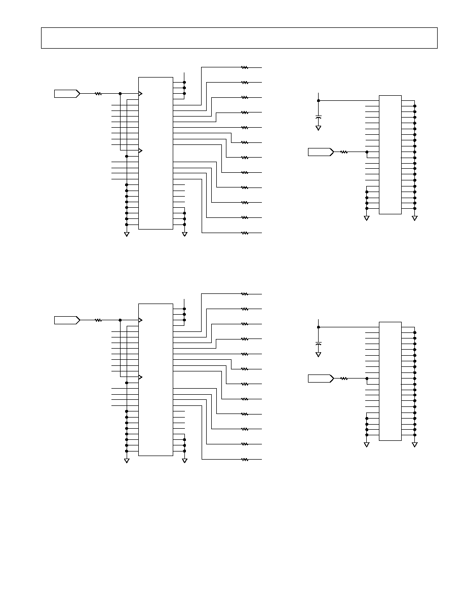
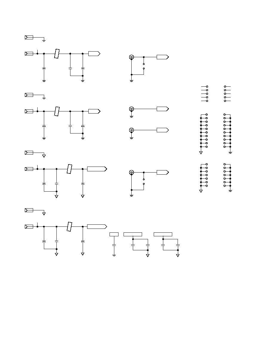
Figure 5a. Evaluation Board Schematic
REV. 0
AD10201
≠14≠
JP1
AINA1
AGNDA
E4
AGNDA
E6
AGNDA
5VAA
C3
10 F
16V
1
2
L3
47 @ 100MHz
C20
0.1 F
C11
10 F
16V
AGNDA
5VAA
+
+
A
IN
A1
J3
AINA2
AGNDA
A
IN
A2
J4
E3
AGNDB
E5
AGNDB
5VAB
C4
10 F
16V
1
2
L4
47 @ 100MHz
C21
0.1 F
C19
10 F
16V
AGNDB
5VAB
+
+
AINB2
AGNDB
A
IN
B2
J7
JP2
AINB1
AGNDB
DGNDA
E34
DGNDA
E25
3.3VDA
C29
10 F
16V
1
2
L1
47 @ 100MHz
C12
0.1 F
C31
10 F
16V
DGNDA
+
+
DUT_3.3VDA
A
IN
B1
J6
DGNDB
E33
DGNDB
E26
3.3VDB
C30
10 F
16V
1
2
L2
47 @ 100MHz
C16
0.1 F
C32
10 F
16V
DGNDB
+
+
DUT_3.3VDB
AGNDA
C34
0.1 F
5VAA
DGNDA
C9
0.1 F
C10
0.1 F
DUT_3.3VDA
DGNDB
C17
0.1 F
C18
0.1 F
DUT_3.3VDB
E30
E29
E35
E36
E37
E38
E39
E40
E46
E45
E80
E79
E83
E84
AGNDB
DGNDB
E41
E42
E43
E44
E47
E48
E65
E66
E68
E67
E69
E70
E71
E72
AGNDA
DGNDA
E74
E73
E75
E76
E82
E81
STITCHES TO TIE GROUNDS TOGETHER
E78
E77
E7
E12
E10
E9
E8
E11
E1
E2
DGNDA
DGNDB
DGNDA
DGNDB
DGNDA
AGNDA
AGNDA
AGNDB
DGNDB
AGNDB
Figure 5b. Evaluation Board Schematic

REV. 0
AD10201
≠15≠
NC
VCC
U2
D
Q
D
Q
VBB
VEE
3
2
1
4
6
7
8
5
MC10EP16D
AGNDA
C13
0.1 F
25V
R42
100
R43
100
AGNDA
R56
33k
3.3VA
C1
0.1 F
R1
51
AGNDA
AGNDA
J5
ENCODE
IN
OUT
SD
NR
ERR
GND
U14
6
2
1
5
3
AGNDA
5VAA
3.3VA
NC
VCC
U3
D
Q
D
Q
VBB
VEE
3
2
1
4
6
7
8
5
MC10EP16D
DGNDA
C6
0.1 F
R3
100
R4
100
DGNDA
R58
33k
3.3VDA
C2
0.1 F
R41
51
AGNDA
AGNDA
J12
ENCA
3.3VDA
D0
VCC
U4
D0
Q
D1
Q
D1
GND
3
2
1
4
6
7
8
5
SY100EPT23L
DGNDA
C5
0.1 F
3.3VDA
LATCHA
BUFLATA
E23
E19
C7
0.1 F
C8
0.1 F
ENCAB
ENCA
NC
VCC
U11
D
Q
D
Q
VBB
VEE
3
2
1
4
6
7
8
5
MC10EP16D
AGNDB
C27
0.47 F
25V
R63
100
R64
100
AGNDB
R38
33k
3.3VB
C22
0.1 F
R60
51
AGNDB
AGNDB
J10
ENCODE
IN
OUT
SD
NR
ERR
GND
U15
6
2
1
5
3
AGNDB
5VAB
3.3VB
NC
VCC
U9
D
Q
D
Q
VBB
VEE
3
2
1
4
6
7
8
5
MC10EP16D
DGNDB
C25
0.1 F
R65
100
R66
100
DGNDB
R39
33k
3.3VDB
C23
0.1 F
R61
51
AGNDB
AGNDB
J11
ENCB
3.3VDB
D0
VCC
U10
D0
Q
D1
Q
D1
GND
3
2
1
4
6
7
8
5
SY100EPT23L
DGNDB
C26
0.1 F
3.3VDB
LATCHB
BUFLATB
E24
E22
C24
0.1 F
C28
0.1 F
ENCBB
ENCB
4
4
Figure 5c. Evaluation Board Schematic

REV. 0
AD10201
≠16≠
AB25
AB24
AB23
AB22
AE15
AD15
AC
1
5
AB15
AE16
AD16
AC
1
6
AB16
AE17
AD17
AC
1
7
AB17
AE18
AD18
AC
1
8
AB18
AE19
AD19
AC
1
9
AB19
AE20
AD20
AC
2
0
AB20
Y25
Y24
Y23
Y22
W25
W24
W23
W22
V25
V24
V23
V22
U25
U24
U23
U22
T25
T24
T23
T22
R25
R24
R23
R22
M25
M24
M23
M22
L25
L24
L23
L22
J25
J24
J23
J22
D20
C20
B20
A20
D19
C19
B19
A19
AI
N
B
2
AI
N
B
1
ENCBB
ENCB
D0B
D1B
D2B
D3B
D4B
D5B
D6B
D7B
D8B
D9B
D10B
D11B
OV
R
B
AGNDB
C35
0.1 F
E50
AGNDA
AGNDA
AGNDA
AGNDA
AGNDA
AGNDA
AGNDA
AGNDA
AGNDA
AGNDA
AGNDA
AGNDA
AGNDA
AGNDA
AGNDA
AGNDA
AGNDA
AGNDA
AGNDA
AGNDA
AGNDA
AGNDA
AGNDA
AGNDA
AGNDA
AGNDA
AGNDA
AGNDA
AGNDA
AGNDA
AGNDA
AGNDA
AGNDA
AGNDA
AGNDA
AGNDA
AGNDA
AGNDA
AGNDA
AGNDA
AGNDA
AGNDA
AGNDA
AGNDA
AGNDA
AGNDA
AGNDA
AGNDA
AGNDA
AGNDA
AGNDA
AGNDA
AGNDA
AGNDA
AGNDA
AGNDA
AGNDA
AGNDA
AGNDA
AGNDA
AGNDA
AGNDA
AGNDA
AGNDA
AGNDA
AGNDA
AGNDA
AGNDA
AGNDA
AGNDA
AGNDA
AGNDA
AGNDA
AGNDA
AGNDA
AGNDA
AGNDA
DGNDA
DGNDA
DGNDA
DGNDA
DGNDA
DGNDA
DGNDA
DGNDA
DGNDA
DGNDA
DGNDA
DGNDA
DGNDA
DGNDA
DGNDA
DGNDA
DGNDA
DGNDA
DGNDA
DGNDA
DGNDA
DGNDA
DGNDA
DGNDA
DGNDB
DGNDB
DGNDB
DGNDB
DGNDB
DGNDB
DGNDB
DGNDB
DGNDB
DGNDB
DGNDB
DGNDB
DGNDB
DGNDB
DGNDB
DGNDB
DGNDB
DGNDB
DGNDB
DGNDB
DGNDB
DGNDB
DGNDB
DGNDB
A1
A2
A3
A4
A5
A6
A9
A12
B1
B2
B3
B4
B5
B6
B9
B12
C1
C2
C3
C4
C5
C6
C9
C12
D1
D2
D3
D4
D5
D6
D9
D12
E1
E2
E3
E4
F1
F2
F3
F4
G1
G2
G3
G4
H1
H2
H3
H4
K1
K2
K3
K4
K10
K11
K12
L1
L2
L3
L4
L10
L11
L12
M10
M11
M12
N10
N11
N12
P1
P2
P3
P4
P10
P11
P12
R10
R11
R12
T10
T11
T12
AA1
AA2
AA3
AA4
AB5
AB13
AC1
AC2
AC3
AC4
AC5
AC13
AD1
AD2
AD3
AD4
AD5
AD13
AE1
AE2
AE3
AE4
AE5
AE13
AA22
AA23
AA24
AA25
AB14
AB21
AC14
AC21
AC22
AC23
AC24
AC25
AD14
AD21
AD22
AD23
AD24
AD25
AE14
AE21
AE22
AE23
AE24
AE25
AGNDA
DGNDA
DGNDB
OV
R
B
OV
R
B
OV
R
B
OV
R
B
D11B (MSBB
)
D11B (MSBB
)
D11B (MSBB
)
D11B (MSBB
)
D10B
D10B
D10B
D10B
D9B
D9B
D9B
D9B
D8B
D8B
D8B
D8B
D7B
D7B
D7B
D7B
D6B
D6B
D6B
D6B
D5B
D5B
D5B
D5B
D4B
D4B
D4B
D4B
D3B
D3B
D3B
D3B
D2B
D2B
D2B
D2B
D1B
D1B
D1B
D1B
D0B (LSBB
)
D0B (LSBB
)
D0B (LSBB
)
D0B (LSBB
)
ENCB
ENCB
ENCB
ENCB
ENCBB
ENCBB
ENCBB
ENCBB
REF_B
REF_B
REF_B
REF_B
AINB1
AINB1
AINB1
AINB1
AINB2
AINB2
AINB2
AINB2
JP4
AGNDA
C36
0.047 F
AGNDA
JP6
AGNDA
JP3
AGNDA
+5VAA
5VAA
5VAA
5VAA
5VAA
5VAA
5VAA
5VAA
5VAA
3.3VDA
3.3VDA
3.3VDA
3.3VDA
SHEILD
SHEILD
SHEILD
SHEILD
SHEILD
SHEILD
SHEILD
SHEILD
SHEILD
SHEILD
SHEILD
3.3VDB
3.3VDB
3.3VDB
3.3VDB
5VAB
5VAB
5VAB
5VAB
5VAB
5VAB
5VAB
5VAB
AGNDB
AGNDB
AGNDB
AGNDB
AGNDB
AGNDB
AGNDB
AGNDB
AGNDB
AGNDB
AGNDB
AGNDB
AGNDB
AGNDB
AGNDB
AGNDB
AGNDB
AGNDB
AGNDB
AGNDB
AGNDB
AGNDB
AGNDB
AGNDB
AGNDB
AGNDB
AGNDB
AGNDB
AGNDB
AGNDB
AGNDB
AGNDB
AGNDB
AGNDB
AGNDB
AGNDB
AGNDB
AGNDB
AGNDB
AGNDB
AGNDB
AGNDB
AGNDB
AGNDB
AGNDB
AGNDB
AGNDB
AGNDB
AGNDB
AGNDB
AGNDB
AGNDB
AGNDB
AGNDB
AGNDB
AGNDB
AGNDB
AGNDB
AGNDB
AGNDB
AGNDB
AGNDB
AGNDB
AGNDB
AGNDB
AGNDB
AGNDB
AGNDB
AGNDB
AGNDB
AGNDB
AGNDB
AGNDB
J1
J2
J3
J4
A10
B10
C10
D10
R1
R2
R3
R4
A13
B13
C13
D13
K13
L13
M13
N13
P13
R13
T13
P22
P23
P24
P25
A16
B16
C16
D16
A18
B18
C18
D18
A14
A15
A17
A21
A22
A23
A24
A25
B14
B15
B17
B21
B22
B23
B24
B25
C14
C15
C17
C21
C22
C23
C24
C25
D14
D15
D17
D21
D22
D23
D24
D25
E22
E23
E24
E25
F22
F23
F24
F25
G22
G23
G24
G25
H22
H23
H24
H25
K14
K15
K16
K22
K23
K24
K25
L14
L15
L16
M14
M15
M16
N14
N15
N16
N22
N23
N24
N25
P14
P15
P16
R14
R15
R16
T14
T15
T16
AGNDB
JP12
AGNDB
JP9
AGNDB
JP8
AGNDB
C37
0.047 F
+5VAA
DUT_3.3VDA
DUT_3.3VDB
+5VAB
OV
R
A
OV
R
A
OV
R
A
OV
R
A
D0A (LSB
A
)
D0A (LSB
A
)
D0A (LSB
A
)
D0A (LSB
A
)
D1A
D1A
D1A
D1A
D2A
D2A
D2A
D2A
D3A
D3A
D3A
D3A
D4A
D4A
D4A
D4A
D5A
D5A
D5A
D5A
D6A
D6A
D6A
D6A
D7A
D7A
D7A
D7A
D8A
D8A
D8A
D8A
D9A
D9A
D9A
D9A
D10A
D10A
D10A
D10A
D11A (MSB
A
)
D11A (MSB
A
)
D11A (MSB
A
)
D11A (MSB
A
)
ENCA
ENCA
ENCA
ENCA
ENCAB
ENCAB
ENCAB
ENCAB
AINA2
AINA2
AINA2
AINA2
AINA1
AINA1
AINA1
AINA1
REF_A
REF_A
REF_A
REF_A
AB4
AB3
AB2
AB1
AE12
AD12
AC
1
2
AB12
AE11
AD11
AC
1
1
AB11
AE10
AD10
AC
1
0
AB10
AE9
AD9
AC
9
AB9
AE8
AD8
AC
8
AB8
AE7
AD7
AC
7
AB7
AE6
AD6
AC
6
AB6
Y4
Y3
Y2
Y1
W4
W3
W2
W1
V4
V3
V2
V1
U4
U3
U2
U1
T4
T3
T2
T1
N4
N3
N2
N1
M4
M3
M2
M1
D7
C7
B7
A7
D8
C8
B8
A8
D11
C11
B11
A11
AI
N
A
1
AI
N
A
2
AGNDA
C33
0.1 F
E49
OV
R
A
D0A
D1A
D2A
D3A
D4A
D5A
D6A
D7A
D8A
D9A
D10A
D11A
ENCA
ENCAB
AD10201
+5VAA
+5VAA
+5VAA
+5VAB
+5VAB
+5VAB
+5VAB
Figure 5d. Evaluation Board Schematic

REV. 0
AD10201
≠17≠
+5V
AA
+
C3
E39
+
J7
+
E4
JP1
E49
J3
J10
J11
E9
E70
E73
E42
E44
E10
E66
E84
E45
E79
E38
+
E23
GND TIE
E24
E22
L2
C12
R23
R11
R10
+
C30
C16
E25
+
C29
R15
R46
R27
R28
+
R16
R40
R9
R25
E7
E6
E47
+
+5VAB
E3
ENCA
J5
E50
U1
J12
ENCA
GND
TIES
E76
E81
E72
E67
E36
E1
E29
E19
C31
L1
E26
E12
R24
GS03983 REV: A
AD10201/ AD10206
EVALUATION BOARD
GND TIE
GND TIE
E11
AGNDA
C11
A
IN
A2
J4
A
IN
A1
A
IN
B1
A
IN
B2
J6
ENCB
L4
E69
E74
E43
E41
E65
E83
E46
ENCB
E80
E35
E37
E34 DGNDA
LATCHA
BUFLATA
E78
LATCHB
+3.3VDA
J1
GND TIE
L3
E8
E5
REF_A
JP2
C19
C4
AGNDB
E75
GND
TIES
E71
E68
E82
E2
E30
R13
R14
E77
BUFLATB
R30
C32
R29
E33 DGNDB
R17
R18
R45
R44
R36
R35
R12
R26
+3.3VDB
J2
REF_B
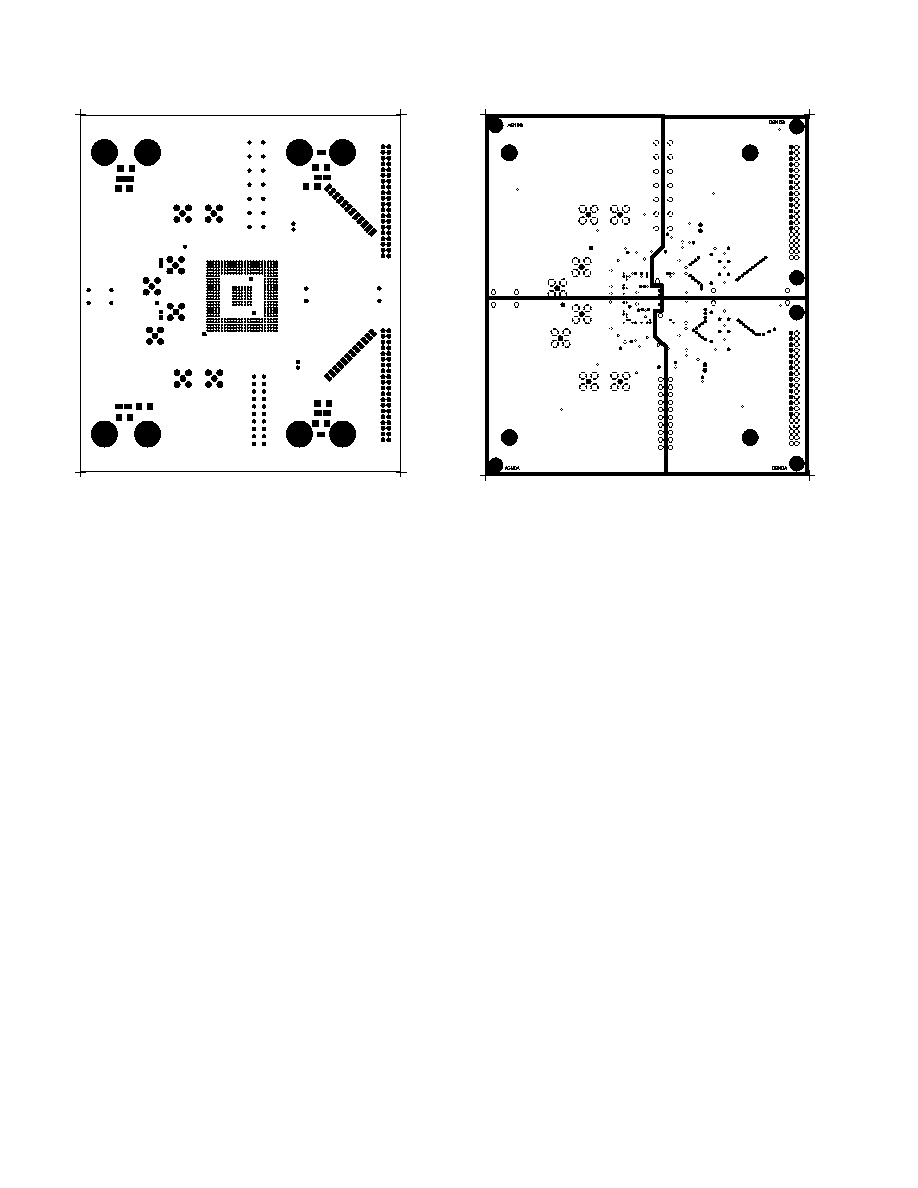
Figure 6a. Mechanical Layout Top View
GND TIE
+
U16
C5
R66
R65
U10
C10
U9
C8
JP9
R64
C28
U14
C13
C36
C37
U15
R63
R56
C1
C22
R60
GND TIE
C9
R8
C26
C25
GND
TIES
U3
GND
TIES
U2
JP4
C23
C34
R1
U17
R72
C6
R4
R3
GND TIE
R39
C2
R41
R42
+5V
JP3
JP6
C21
C35
C18
C24
C27
U11
GND TIE
R71
C15
C14
U4
R7
C17
C7
R43
R58
C33
C20
JP8
JP12
R38
R61
Figure 6b. Mechanical Layout Bottom View
Figure 6c. Top View
Figure 6d. Layer 2
REV. 0
AD10201
≠18≠
Figure 6e. Layer 3
Figure 6f. Bottom View

REV. 0
AD10201
≠19≠
OUTLINE DIMENSIONS
Dimensions shown in millimeters (mm).
385-Lead Ball Grid Array (BGA)
(B-385)
AD10201AB
XXXX
DETAIL C
0.75
0.60
0.50
DETAIL A
0.90
0.75
0.60
DETAIL B
AD10201AB
XXXX
DETAIL C
37.00
35.00 BSC SQ
33.00
DETAIL A
1.27 TYP
A
C
E
G
J
L
N
R
U
W
AA
AC
B
D
F
H
K
M
P
T
V
Y
AB
AD
AE
1
3
5
7
9
11
13
15
17
19
21
23
25
2
4
6
8
10
12
14
16
18
20
22
24
DETAIL B
30.48 BSC
SQ
COMPONENT
VOLUME
1.15
1.02
0.89
3.20
MAX

≠20≠
C02860≠0≠5/02(0)
PRINTED IN U.S.A.