 | –≠–ª–µ–∫—Ç—Ä–æ–Ω–Ω—ã–π –∫–æ–º–ø–æ–Ω–µ–Ω—Ç: AD15452 | –°–∫–∞—á–∞—Ç—å:  PDF PDF  ZIP ZIP |
3-Channel, Low Noise, Low Power, 16-/24-Bit
Sigma-Delta ADC with On-Chip In-Amp
AD7798/AD7799
Rev. 0
Information furnished by Analog Devices is believed to be accurate and reliable.
However, no responsibility is assumed by Analog Devices for its use, nor for any
infringements of patents or other rights of third parties that may result from its use.
Specifications subject to change without notice. No license is granted by implication
or otherwise under any patent or patent rights of Analog Devices. Trademarks and
registered trademarks are the property of their respective owners.
One Technology Way, P.O. Box 9106, Norwood, MA 02062-9106, U.S.A.
Tel: 781.329.4700
www.analog.com
Fax: 781.326.8703
© 2005 Analog Devices, Inc. All rights reserved.
FEATURES
RMS noise:
27 nV at 4.17 Hz (AD7799)
65 nV at 16.7 Hz (AD7799)
40 nV at 4.17 Hz (AD7798)
85 nV at 16.7 Hz (AD7798)
Current: 380 µA typ
Power-down: 1 µA max
Low noise programmable gain instrumentation-amp
Update rate: 4.17 Hz to 500 Hz
3 differential inputs
Internal clock oscillator
Simultaneous 50 Hz/60 Hz rejection
Reference Detect
Low-side power switch
Programmable digital outputs
Burnout currents
Power supply: 2.7 V to 5.25 V
≠40∞C to +105∞C temperature range
Independent interface power supply
16-lead TSSOP package
INTERFACE
3-wire serial
SPIÆ-, QSPITM-, MICROWIRETM-, and DSP-compatible
Schmitt trigger on SCLK
APPLICATIONS
Weigh scales
Pressure measurement
Strain gauge transducers
Gas analysis
Industrial process control
Instrumentation
Portable instrumentation
Blood analysis
Smart transmitters
Liquid/gas chromotography
6-digit DVM
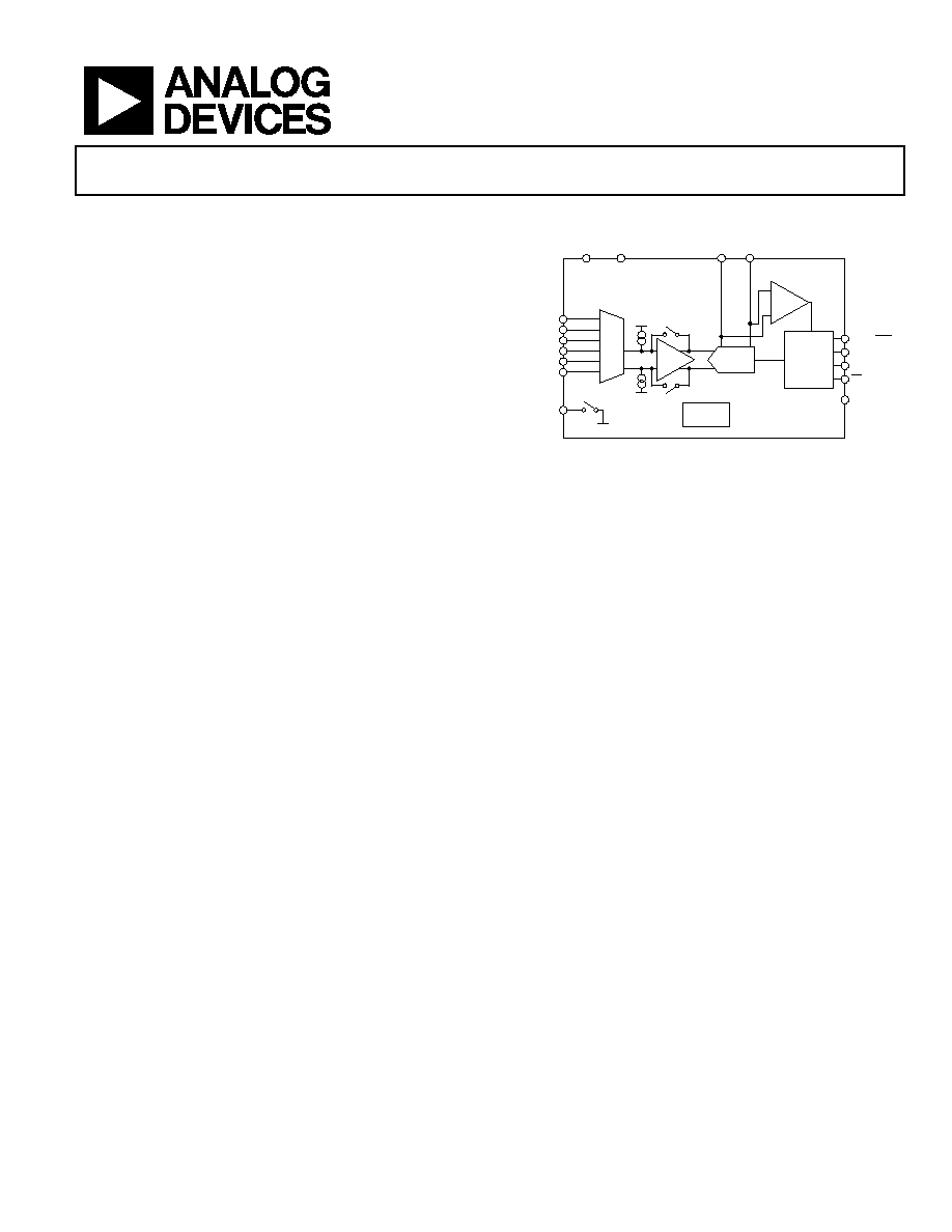
FUNCTIONAL BLOCK DIAGRAM
04856-001
DOUT/RDY
DIN
SCLK
CS
DV
DD
SERIAL
INTERFACE
AND
CONTROL
LOGIC
-
ADC
AD7798/AD7799
AD7798: 16-BIT
AD7799: 24-BIT
AIN2(+)
AIN2(≠)
AIN3(+)/P1
AIN1(+)
AIN1(≠)
AIN3(≠)/P2
AV
DD
GND
MUX
INTERNAL
CLOCK
GND
GND
AV
DD
REFIN(≠)
PSW
IN-AMP
REFERENCE
DETECT
REFIN(+)
Figure 1.
GENERAL DESCRIPTION
The AD7798/AD7799 are low power, low noise, complete
analog front ends for high precision measurement applications.
The AD7798/AD7799 contains a low noise, 16-/24-bit -
ADC with three differential analog inputs. The on-chip, low
noise instrumentation amplifier means that signals of small
amplitude can be interfaced directly to the ADC. With a gain
setting of 64, the rms noise is 27 nV for the AD7799 and 40 nV
for the AD7798 when the update rate equals 4.17 Hz.
On-chip features include a low-side power switch, reference
detect, programmable digital output pins, burnout currents,
and an internal clock oscillator. The output data rate from the
part is software-programmable and can be varied from 4.17 Hz
to 500 Hz.
The part operates with a power supply from 2.7 V to 5.25 V.
The AD7798 consumes a current of 300 µA typical, whereas the
AD7799 consumes 380 µA typical. Both devices are housed in a
16-lead TSSOP package.

AD7798/AD7799
Rev. 0 | Page 2 of 28
TABLE OF CONTENTS
Specifications..................................................................................... 3
Timing Characteristics..................................................................... 6
Absolute Maximum Ratings............................................................ 8
ESD Caution.................................................................................. 8
Pin Configuration and Function Descriptions............................. 9
Output Noise and Resolution Specifications .............................. 10
AD7798 ........................................................................................ 10
AD7799 ........................................................................................ 11
Typical Performance Characteristics ........................................... 12
On-Chip Registers .......................................................................... 13
Communication Register .......................................................... 13
Status Register ............................................................................. 14
Mode Register ............................................................................. 14
Configuration Register .............................................................. 16
Data Register ............................................................................... 17
ID Register................................................................................... 17
IO Register................................................................................... 17
Offset Register............................................................................. 18
Full-Scale Register ...................................................................... 18
ADC Circuit Information.............................................................. 19
Overview ..................................................................................... 19
Digital Interface.......................................................................... 20
Circuit Description......................................................................... 23
Analog Input Channel ............................................................... 23
Instrumentation Amplifier........................................................ 23
Bipolar/Unipolar Configuration .............................................. 23
Data Output Coding .................................................................. 24
Burnout Currents ....................................................................... 24
Reference ..................................................................................... 24
Reference Detect......................................................................... 24
Reset ............................................................................................. 25
AV
DD
Monitor ............................................................................. 25
Calibration................................................................................... 25
Grounding and Layout .............................................................. 26
Applications..................................................................................... 27
Weigh Scales................................................................................ 27
Outline Dimensions ....................................................................... 28
Ordering Guide .......................................................................... 28
REVISION HISTORY
1/05--Revision 0: Initial Version

AD7798/AD7799
Rev. 0 | Page 3 of 28
SPECIFICATIONS
AV
DD
= 2.7 V to 5.25 V; DV
DD
= 2.7 V to 5.25 V; GND = 0 V; REFIN(+) = AV
DD
; REFIN(-) = 0 V. All specifications T
MIN
to T
MAX
, unless
otherwise noted.
Table 1.
Parameter
AD7798B/AD7799B
1
Unit
Test Conditions/Comments
ADC CHANNEL
Output Update Rate
4.17 - 500
Hz nom
No Missing Codes
2
24
Bits min
AD7799: f
ADC
< 250 Hz
16
Bits min
AD7798
Resolution
See Table 5 to Table 8
Output Noise and Update Rates
See Table 5 to Table 8
Integral Nonlinearity
±15
ppm of FSR max
Offset Error
3
±1
µV typ
Offset Error Drift vs. Temperature
4
±10
nV/∞C typ
Full-Scale Error
3, 5
±10
µV typ
Gain Drift vs. Temperature
4
±1
ppm/∞C typ
Power Supply Rejection
100
dB min
AIN = 1 V/gain, gain 4
ANALOG INPUTS
Differential Input Voltage Ranges
±V
REF
/gain
V nom
V
REF
= REFIN(+) ≠ REFIN(≠), gain = 1 to 128
Absolute AIN Voltage Limits
2
Unbuffered Mode
GND - 30 mV
V min
Gain = 1 or 2
AV
DD
+ 30 mV
V max
Buffered Mode
GND + 100 mV
V min
Gain = 1 or 2
AV
DD
≠ 100 mV
V max
In-Amp Active
GND + 300 mV
V min
Gain = 4 to 128
AV
DD
- 1.1
V max
Common-Mode Voltage, V
CM
0.5
V min
V
CM
= (AIN(+) + AIN(-))/2, gain = 4 to 128
Analog Input Current
Buffered Mode or In-Amp Active
Average Input Current
2
±1
nA max
Gain = 1 or 2, update rate < 100 Hz
±250
pA max
Gain = 4 to 128, update rate < 100 Hz
±1
nA max
AIN3(+)/AIN3(-), update rate < 100 Hz
Average Input Current Drift
±2
pA/∞C typ
Unbuffered Mode
Gain = 1 or 2
Average Input Current
±400
nA/V typ
Input current varies with input voltage
Average Input Current Drift
±50
pA/V/∞C typ
Normal-Mode Rejection
2
@ 50 Hz, 60 Hz
65
dB min
80 dB typ, 50 ± 1 Hz, 60 ± 1 Hz (FS[3:0] = 1010)
6
@ 50 Hz
80
dB min
90 dB typ, 50 ± 1 Hz (FS[3:0] = 1001)
6
@ 60 Hz
90
dB min
100 dB typ, 60 ± 1 Hz (FS[3:0] = 1000)
6
Common-Mode Rejection
@ DC
100
dB min
AIN = 1 V/gain, gain 4
@ 50 Hz, 60 Hz
2
100
dB min
50 ± 1 Hz, 60 ± 1 Hz (FS[3:0] = 1010)
6
@ 50 Hz, 60 Hz
2
100
dB min
50 ± 1 Hz (FS[3:0] = 1001
6
), 60 ± 1 Hz
(FS[3:0] = 1000
6
)
AD7798/AD7799
Rev. 0 | Page 4 of 28
Parameter
AD7798B/AD7799B
1
Unit
Test Conditions/Comments
REFERENCE
External REFIN Voltage
2.5
V nom
REFIN = REFIN(+) - REFIN(-)
Reference Voltage Range
2
0.1
V min
AV
DD
V
max
When V
REF
= AV
DD
, the differential input must be
limited to (0.9 x V
REF
/gain) if the in-amp is active.
Absolute REFIN Voltage Limits
2
GND - 30 mV
V min
AV
DD
+ 30 mV
V max
Average Reference Input Current
400
nA/V typ
Average Reference Input Current Drift
±0.03
nA/V/∞C typ
Normal-Mode Rejection
Same as for analog
inputs
Common-Mode Rejection
100
dB typ
Reference Detect Levels
0.3
V min
0.65
V max
NOXREF bit active if V
REF
< 0.3 V
LOW-SIDE POWER SWITCH
R
ON
7
max
AV
DD
= 5 V
9
max
AV
DD
= 3 V
Allowable Current
2
30
mA max
Continuous current
DIGITAL OUTPUTS (P1 and P2)
Output High Voltage, V
OH
2
AV
DD
- 0.6
V min
AV
DD
= 3 V, I
SOURCE
= 100 µA
Output Low Voltage, V
OL
2
0.4
V
max
AV
DD
= 3 V, I
SINK
= 100 µA
Output High Voltage, V
OH
2
4
V min
AV
DD
= 5 V, I
SOURCE
= 200 µA
Output Low Voltage, V
OL
2
0.4
V max
AV
DD
= 5 V, I
SINK
= 800 µA
INTERNAL CLOCK
Frequency
2
64 ± 3%
kHz min/max
LOGIC INPUTS
CS
2
Input Low Voltage, V
INL
0.8
V
max
DV
DD
= 5 V
Input High Voltage, V
INH
0.4
2.0
V max
V min
DV
DD
= 3 V
DV
DD
= 3 V or 5 V
SCLK and DIN
(Schmitt-Triggered Input)
2
V
T
(+) 1.4/2
V
min/max
DV
DD
= 5 V
V
T
(≠) 0.8/1.7
V
min/max
DV
DD
= 5 V
V
T
(+) ≠ V
T
(≠) 0.1/0.17
V
min/max
DV
DD
= 5 V
V
T
(+)
0.9/2
V min/max
DV
DD
= 3 V
V
T
(≠) 0.4/1.35
V
min/max
DV
DD
= 3 V
V
T
(+) - V
T
(≠) 0.06/0.13
V
min/max
DV
DD
= 3 V
Input Currents
±10
µA max
V
IN
= DV
DD
or GND
Input Capacitance
10
pF typ
All digital inputs
LOGIC OUTPUTS
Output High Voltage, V
OH
2
DV
DD
- 0.6
V min
DV
DD
= 3 V, I
SOURCE
= 100 µA
Output Low Voltage, V
OL
2
0.4
V
max
DV
DD
= 3 V, I
SINK
= 100 µA
Output High Voltage, V
OH
2
4
V
min DV
DD
= 5 V, I
SOURCE
= 200 µA
Output Low Voltage, V
OL
2
0.4
V
max
DV
DD
= 5 V, I
SINK
= 1.6 mA
Floating-State Leakage Current
±10
µA max
Floating-State Output Capacitance 10
pF
typ
Data Output Coding
Offset binary
AD7798/AD7799
Rev. 0 | Page 5 of 28
Parameter
AD7798B/AD7799B
1
Unit
Test Conditions/Comments
SYSTEM CALIBRATION
2
Full-Scale Calibration Limit
1.05 ◊ FS
V max
FS = Full scale analog input. When V
REF
= AV
DD
, the
differential input must be limited to (0.9 x V
REF
/gain)
if the in-amp is active.
Zero-Scale Calibration Limit
-1.05 ◊ FS
V min
Input Span
0.8 ◊ FS
V min
2.1 ◊ FS
V max
POWER REQUIREMENTS
7
Power Supply Voltage
AV
DD
≠ GND
2.7/5.25
V min/max
DV
DD
≠ GND
2.7/5.25
V min/max
Power Supply Currents
I
DD
Current
140
µA max
Unbuffered mode, 110 µA typ @ AV
DD
= 3 V,
125 µA typ @ AV
DD
= 5 V
180
µA
max
Buffered mode, Gain = 1 or 2, 130 µA typ @ AV
DD
= 3 V,
165 µA typ @ AV
DD
= 5 V
400
µA
max
AD7798: Gain = 4 to 128, 300 µA typ @ AV
DD
= 3 V,
350 µA typ @ AV
DD
= 5 V
500
µA
max
AD7799: Gain = 4 to 128, 380 µA typ @ AV
DD
= 3 V,
440 µA typ @ AV
DD
= 5 V
I
DD
(Power-Down Mode)
1
µA max
1
Temperature range is ≠40∞C to +105∞C.
2
Specification is not production tested, but is supported by characterization data at initial product release.
3
Following a calibration, this error is in the order of the noise for the programmed gain and update rate selected.
4
Recalibration at any temperature removes these errors.
5
Full-scale error applies to both positive and negative full scale and applies at the factory calibration conditions (AV
DD
= 4 V, gain = 1, T
A
= 25∞C).
6
FS[3:0] are the four bits used in the mode register to select the output word rate.
7
Digital inputs equal to DV
DD
or GND.