PIN CONFIGURATION
SOT-23 Package
1
2
NC = NO CONNECT
V+
NC (OR V≠)
V≠
3
TOP
VIEW
QUANTITY
TEMPERATURE DRIFT ≠ ppm/
∞
C
0
≠40
5
10
15
20
25
30
35
40
45
50
≠30
≠20
≠10
0
10
20
30
40
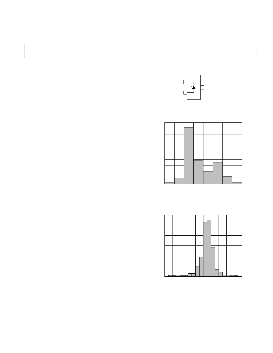
Reverse Voltage Temperature Drift Distribution
QUANTITY
OUTPUT ERROR ≠ mV
0
≠10
50
100
150
200
250
300
≠8
≠6
≠4
≠2
0
2
4
10
6
8
Reverse Voltage Error Distribution
REV. 0
Information furnished by Analog Devices is believed to be accurate and
reliable. However, no responsibility is assumed by Analog Devices for its
use, nor for any infringements of patents or other rights of third parties
which may result from its use. No license is granted by implication or
otherwise under any patent or patent rights of Analog Devices.
a
1.2 V Micropower, Precision
Shunt Voltage Reference
© Analog Devices, Inc., 1995
One Technology Way, P.O. Box 9106, Norwood, MA 02062-9106, U.S.A.
Tel: 617/329-4700
Fax: 617/326-8703
AD1580
FEATURES
Wide Operating Range: 50
A≠10 mA
Initial Accuracy:
0.1% max
Temperature Drift:
50 ppm/ C max
Output Impedance: 0.5
max
Wideband Noise (10 Hz≠10 kHz): 20 V rms
Operating Temperature Range: ≠40 C to +85 C
High ESD Rating
4 kV Human Body Model
400 V Machine Model
Compact, Surface-Mount, SOT-23 Package
GENERAL DESCRIPTION
The AD1580 is a low cost, two-terminal (shunt), precision
bandgap reference. It provides an accurate 1.225 V output for
input currents between 50
µ
A and 10 mA.
The AD1580's superior accuracy and stability is made possible
by the precise matching and thermal tracking of on-chip
components. Proprietary curvature correction design techniques
have been used to minimize the nonlinearities in the voltage
output temperature characteristics. The AD1580 is stable with
any value of capacitive load.
The low minimum operating current makes the AD1580 ideal
for use in battery powered 3 V or 5 V systems. However, the
wide operating current range means that the AD1580 is
extremely versatile and suitable for use in a wide variety of high
current applications.
The AD1580 is available in two grades, A and B, both of which
are provided in an SOT-23 package, the smallest surface mount
package available on the market. Both grades are specified over
the industrial temperature range of ≠40
∞
C to +85
∞
C.
TARGET APPLICATIONS
1. Portable, Battery-Powered Equipment:
Cellular Phones, Notebook Computers, PDAs, GPS and
DMM.
2. Computer Workstations
Suitable for use with a wide range of video RAMDACs.
3. Smart Industrial Transmitters
4. PCMCIA Cards.
5. Automotive.
6. 3 V/5 V 8≠12-Bit Data Converters.
REV. 0
≠2≠
AD1580≠SPECIFICATIONS
Model
AD1580A
AD1580B
Min
Typ
Max
Min
Typ
Max
Units
Reverse Voltage Output
1.215
1.225
1.235
1.224
1.225
1.226
V
Reverse Voltage Temperature Drift
≠40
∞
C to +85
∞
C
100
50
ppm/
∞
C
Minimum Operating Current, T
MIN
to T
MAX
50
50
µ
A
Reverse Voltage Change with Reverse Current
50
µ
A < I
IN
< 10 mA, T
MIN
to T
MAX
2.5
5
2.5
5
mV
50
µ
A < I
IN
< 1 mA, T
MIN
to T
MAX
0.5
0.5
mV
Dynamic Output Impedance (
V
R
/
I
R
)
I
IN
= 1 mA
±
100
µ
A (f = 120 Hz)
0.4
1
0.4
0.5
OUTPUT NOISE
RMS Noise Voltage: 10 Hz to 10 kHz
20
20
µ
V
rms
Low Frequency Noise Voltage: 0.1 Hz to 10 Hz
5
5
µ
V
p-p
Turn-On Settling Time to 0.1%
1
5
5
µ
s
Output Voltage Hysteresis
2
80
80
µ
V
Temperature Range
Specified Performance, T
MIN
to T
MAX
≠40
+85
≠40
+85
∞
C
Operating Range
3
≠55
+125
≠55
+125
∞
C
NOTES
1
Measured with no load capacitor.
2
Output hysteresis is defined as the change in the +25
∞
C output voltage after a temperature excursion to +85
∞
C and then to ≠40
∞
C.
3
The operating temperature range is defined as the temperature extremes at which the device will continue to function. Parts may deviate from their specified
performance.
Specifications subject to change without notice.
(@ T
A
= +25 C, I
IN
= 100 A, unless otherwise noted)
CAUTION
ESD (electrostatic discharge) sensitive device. Electrostatic charges as high as 4000 V readily
accumulate on the human body and test equipment and can discharge without detection. Although
the AD1580 features proprietary ESD protection circuitry, permanent damage may occur on
devices subjected to high energy electrostatic discharges. Therefore, proper ESD precautions are
recommended to avoid performance degradation or loss of functionality.
WARNING!
ESD SENSITIVE DEVICE
ABSOLUTE MAXIMUM RATINGS
1
Reverse Current . . . . . . . . . . . . . . . . . . . . . . . . . . . . . . . 25 mA
Forward Current . . . . . . . . . . . . . . . . . . . . . . . . . . . . . . 20 mA
Internal Power Dissipation
2
SOT-23 (RT) . . . . . . . . . . . . . . . . . . . . . . . . . . . . 0.3 Watts
Storage Temperature Range . . . . . . . . . . . . ≠65
∞
C to +150
∞
C
Operating Temperature Range
AD1580/RT . . . . . . . . . . . . . . . . . . . . . . . ≠ 55
∞
C to +125
∞
C
Lead Temperature, Soldering
Vapor Phase (60 sec) . . . . . . . . . . . . . . . . . . . . . . . . +215
∞
C
Infrared (15 sec) . . . . . . . . . . . . . . . . . . . . . . . . . . . . +220
∞
C
ESD Susceptibility
3
Human Body Model . . . . . . . . . . . . . . . . . . . . . . . . . . 4 kV
Machine Model . . . . . . . . . . . . . . . . . . . . . . . . . . . . . 400 V
NOTES
1
Stresses above those listed under "Absolute Maximum Ratings" may cause
permanent damage to the device. This is a stress rating only and functional
operation of the device at these or any other conditions above those indicated in
the operational section of this specification is not implied. Exposure to absolute
maximum rating conditions for extended periods may affect device reliability.
2
Specification is for device in free air at +25
∞
C: SOT-23 Package:
JA
= 300
∞
C/Watt.
3
The human body model is a 100 pF capacitor discharged through 1.5 k
. For the
machine model, a 200 pF capacitor is discharged directly into the device.
ORDERING GUIDE
Initial Output
Temperature
Package
Model
Error
Coefficient
Option
AD1580ART
10 mV
100 ppm/
∞
C
RT
AD1580ART-REEL
1
10 mV
100 ppm/
∞
C
RT
AD1580ART-REEL7
2
10 mV
100 ppm/
∞
C
RT
AD1580BRT
1 mV
50 ppm/
∞
C
RT
AD1580BRT-REEL
1
1 mV
50 ppm/
∞
C
RT
AD1580BRT-REEL7
2
1 mV
50 ppm/
∞
C
RT
NOTES
1
Provided on a 13-inch reel containing 7,000 pieces.
2
Provided on a 7-inch reel containing 2,000 pieces.
PACKAGE BRANDING INFORMATION
Four marking fields identify the device generic, grade, and date
of processing. The first field is the product identifier. A "0"
identifies the generic as the AD1580. The second field indicates
the device grade; "A" or "B." In the third field a numeral or
letter indicates a calendar year; "5" for 1995, "A" for 2001. In
the fourth field, letters A-Z represent a two week window within
the calendar year; starting with "A" for the first two weeks of
January.
Typical Performance Characteristics≠AD1580
REV. 0
≠3≠
REVERSE VOLTAGE CHANGE ≠ ppm
TEMPERATURE ≠
∞
C
≠2000
≠55
≠1000
≠500
0
500
1000
≠35
≠15
5
25
65
85
125
105
≠1500
45
~
20ppm/
∞
C
Figure 1. Output Drift for Different Temperature
Characteristics
4
3
≠1
2
1
0
REVERSE VOLTAGE CHANGE ≠ mV
0.1
10
1
0.01
REVERSE CURRENT ≠ mA
T
A
= 125
∞
C
T
A
=
≠40
∞
C ≠ +85
∞
C
Figure 2. Output Voltage Error vs. Reverse Current
FREQUENCY ≠ Hz
1.0
10
100
1k
10k
100k
1M
600
200
400
NOISE VOLTAGE ≠ nV/
Hz
Figure 3. Noise Spectral Density
REVERSE VOLTAGE ≠ V
REVERSE CURRENT ≠ µA
100
0
0
1.4
0.2
0.4
0.6
0.8
1.0
1.2
40
20
80
60
+85
∞
C
+25
∞
C
≠40
∞
C
Figure 4. Reverse Current vs. Reverse Voltage
FORWARD CURRENT ≠ mA
1.0
0
0.01
100
FORWARD VOLTAGE ≠ V
0.1
1
10
0.4
0.2
0.8
0.6
+25
∞
C
+85
∞
C
≠40
∞
C
Figure 5. Forward Voltage vs. Forward Current
AD1580
REV. 0
≠4≠
THEORY OF OPERATION
The AD1580 uses the "bandgap" concept to produce a stable,
low temperature coefficient voltage reference suitable for high
accuracy data acquisition components and systems. The device
makes use of the underlying physical nature of a silicon
transistor base-emitter voltage in the forward-biased operating
region. All such transistors have approximately a ≠2 mV/
∞
C
temperature coefficient, unsuitable for use directly as a low TC
reference; however, extrapolation of the temperature characteristic
of any one of these devices to absolute zero (with collector
current proportional to absolute temperature) reveals that its
V
BE
will go to approximately the silicon bandgap voltage. Thus,
if a voltage could be developed with an opposing temperature
coefficient to sum with V
BE
, a zero TC reference would result.
The AD1580 circuit in Figure 6, provides such a compensating
voltage, V1 by driving two transistors at different current
densities and amplifying the resultant V
BE
difference (
V
BE
--
which has a positive TC). The sum of V
BE
and V1 provide a
stable voltage reference.
V+
V≠
V1
V
BE
V
BE
Figure 6. Schematic Diagram
APPLYING THE AD1580
The AD1580 is simple to use in virtually all applications. To
operate the AD1580 as a conventional shunt regulator (Figure
7a), an external series resistor is connected between the supply
voltage and the AD1580. For a given supply voltage the series
resistor, R
S
, determines the reverse current flowing through the
AD1580. The value of R
S
must be chosen to accommodate the
expected variations of the supply voltage, V
S
, load current, I
L
,
and the AD1580 reverse voltage, V
R
, while maintaining an
acceptable reverse current, I
R
, through the AD1580.
The minimum value for R
S
should be chosen when V
S
is at
its minimum, and I
L
and V
R
are at their maximum while
maintaining the minimum acceptable reverse current.
The value of R
S
should be large enough to limit I
R
to 10 mA
when V
S
is at its maximum, and I
L
and V
R
are at their minimum.
The equation for selecting R
S
is as follows:
R
S
= (V
S
≠ V
R
)/(I
R
+ I
L
)
Figure 7b shows a typical connection with the AD1580BRT
operating at a minimum of 100
µ
A that can provide
±
1 mA to
its load, while accommodating
±
10% power supply variations.
V
S
+5V(+3V)
±
10%
I
R
V
R
I
R +
I
L
I
L
R
S
V
R
R
S
V
OUT
(a)
(b)
V
OUT
2.94k
(1.30k
)
Figure 7. Typical Connection Diagram
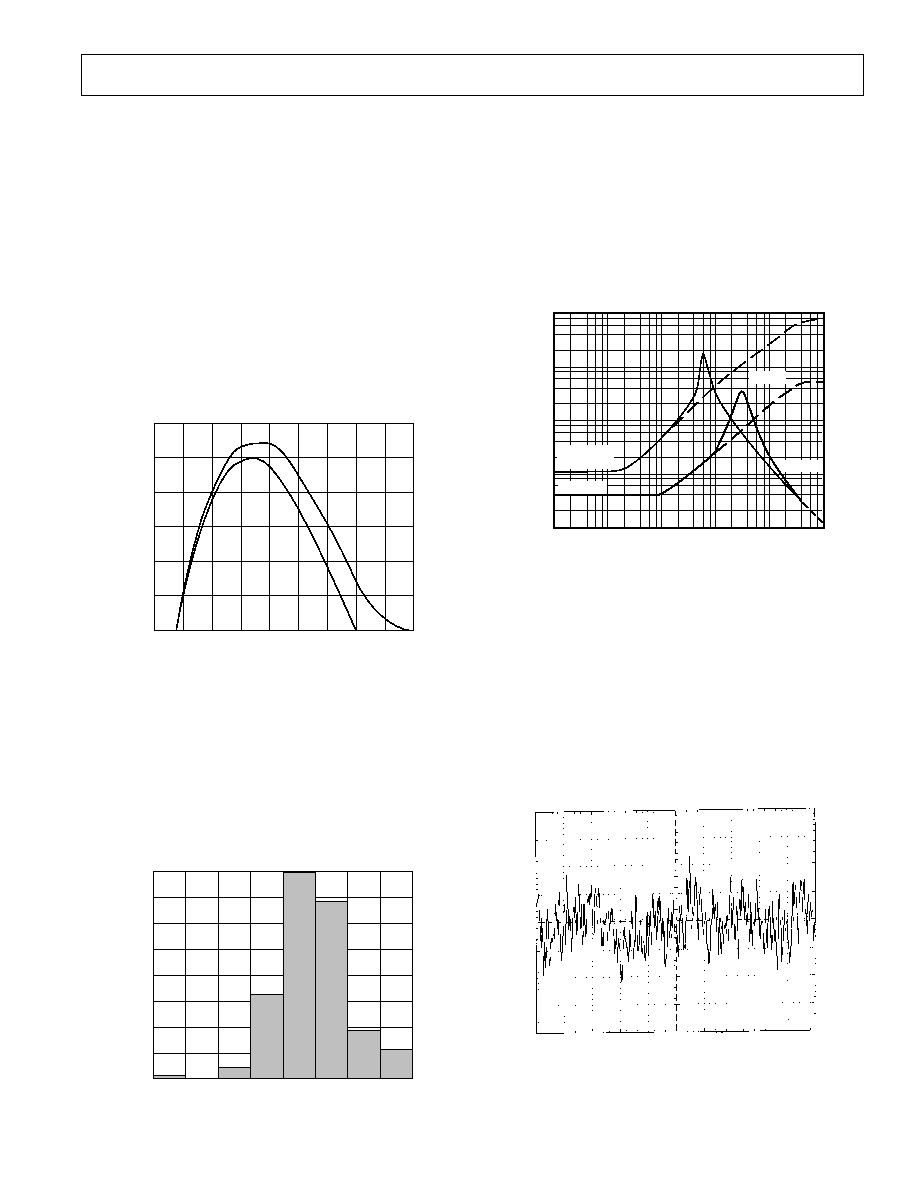
TEMPERATURE PERFORMANCE
The AD1580 is designed for reference applications where
stable temperature performance is important. Extensive
temperature testing and characterization ensures that the device's
performance is maintained over the specified temperature range.
Some confusion exists in the area of defining and specifying
reference voltage error over temperature. Historically, references
have been characterized using a maximum deviation per degree
centigrade, i.e., 50 ppm/
∞
C. However, because of nonlinearities
in temperature characteristics which originated in standard
Zener references (such as "S" type characteristics), most
manufacturers now use a maximum limit error band approach
to specify devices. This technique involves the measurement of
the output at three or more different temperatures to guarantee
that the voltage will fall within the given error band. The
proprietary curvature correction design techniques used to
minimize the AD1580 nonlinearities allow the temperature
performance to be guaranteed using the maximum deviation
method. This method is of more use to a designer than the one
which simply guarantees the maximum error band over the
entire temperature change.
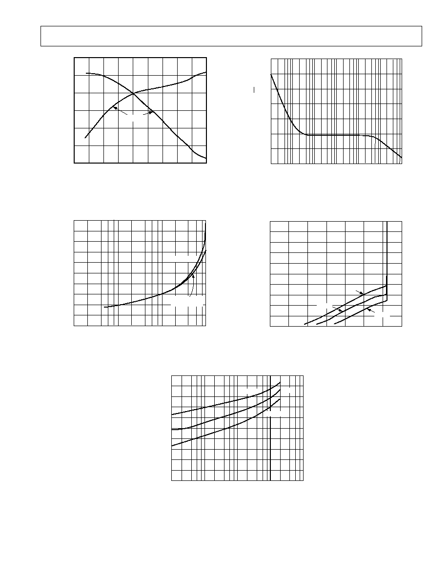
Figure 8 shows a typical output voltage drift for the AD1580
and illustrates the methodology. The maximum slope of the
two diagonals drawn from the initial output value at 25
∞
C to the
output values at 85
∞
C and ≠40
∞
C determines the performance
grade of the device. For a given grade of the AD1580 the
designer can easily determine the maximum total error from the
initial tolerance plus temperature variation. For example, the
AD1580BRT initial tolerance is
±
1 mV, a
±
50 ppm/
∞
C
temperature coefficient corresponds to an error band of
±
4 mV
OUTPUT VOLTAGE ≠ V
TEMPERATURE ≠
∞
C
1.2238
≠55
1.2248
1.2250
1.2252
1.2254
1.2256
1.2258
≠35
≠15
5
25
65
85
125
105
1.2244
1.2246
1.2240
1.2242
45
V
MIN
V
O
V
MAX
SLOPE = TC = ----------------------≠≠≠≠
(V
MAX
≠ V
O
)
(85
∞
C ≠ 25
∞
C) x 1.225 x 10
≠6
SLOPE = TC = ----------------------≠≠≠≠≠
(≠40
∞
C ≠ 25
∞
C) x 1.225 x 10
≠6
(V
MIN
≠ V
O
)
Figure 8. Output Voltage vs. Temperature
AD1580
REV. 0
≠5≠
(50
◊
10
≠6
◊
1.225 V
◊
65
∞
C) thus, the unit is guaranteed to be
1.225 V
±
5 mV over the operating temperature range.
Duplication of these results requires a combination of high
accuracy and stable temperature control in a test system.
Evaluation of the AD1580 will produce a curve similar to that in
Figures 1 and 8.
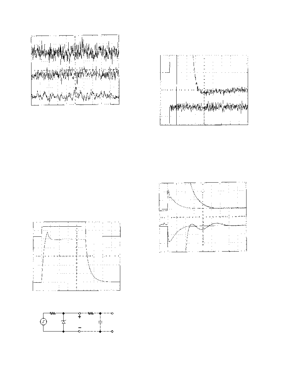
VOLTAGE OUTPUT NONLINEARITY VERSUS
TEMPERATURE
When using a reference with data converters it is important to
understand how temperature drift affects the overall converter
performance. The nonlinearity of the reference output drift
represents additional error that is not easily calibrated out of the
system. This characteristic (Figure 9) is generated by normal-
izing the measured drift characteristic to the end point average
drift. The residual drift error of approximately 500 ppm shows
that the AD1580 is compatible with systems that require 10-bit
accurate temperature performance.
TEMPERATURE ≠
∞
C
600
300
0
≠55
125
≠35
RESIDUAL DRIFT ERROR ≠ ppm
≠15
5
25
45
65
85
105
500
400
200
100
Figure 9. Residual Drift Error
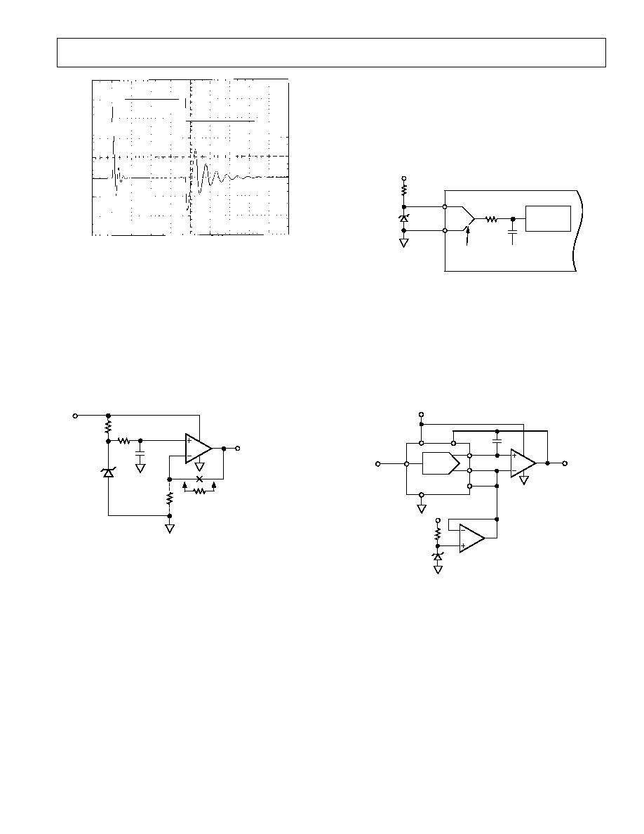
REVERSE VOLTAGE HYSTERESIS
A major requirement for high performance industrial equipment
manufacturers is a consistent output voltage at nominal tempera-
ture following operation over the operating temperature range.
This characteristic is generated by measuring the difference
between the output voltage at +25
∞
C after operation at +85
∞
C,
and the output, also at +25
∞
C after operation at ≠40
∞
C. Figure 10
displays the hysteresis associated with AD1580. This characteristic
exists in all references and has been minimized in the AD1580.
QUANTITY
HYSTERESIS VOLTAGE ≠ µV
0
≠400
15
20
25
30
35
40
≠300
≠200
≠100
0
100
200
400
300
5
10
Figure 10. Reverse Voltage Hysteresis Distribution
OUTPUT IMPEDANCE VERSUS FREQUENCY
Understanding the effect of the reverse dynamic output
impedance in a practical application may be important to
successfully apply the AD1580. A voltage divider is formed by
the AD1580's output impedance and the external source
impedance. When using an external source resistor of about
30 k
(I
R
= 100
µ
A), 1% of the noise from a 100 kHz switching
power supply is developed at the output of the AD1580. Figure
11 shows how a 1
µ
F load capacitor connected directly across
the AD1580 reduces the affect of power supply noise to less
than 0.01%.
1k
10
OUTPUT IMPEDANCE ≠
0.1
100
100k
10k
1k
10
1
100
FREQUENCY ≠ Hz
1M
I
R
= 0.1I
R
I
R
= 100µA
I
R
= 1mA
C
L
= 0
C
L
= 1µF
Figure 11. Output Impedance vs. Frequency
NOISE PERFORMANCE AND REDUCTION
The noise generated by the AD1580 is typically less than 5
µ
V p-p
over the 0.1 Hz to 10 Hz band. Figure 12 shows the 0.1 Hz to
10 Hz noise of a typical AD1580. Noise in a 10 Hz≠10 kHz
bandwidth is approximately 20
µ
V rms (Figure 13a). If further
noise reduction is desired, a 1-pole low-pass filter may be added
between the output pin and ground. A time constant of 0.2 ms
will have a ≠3 dB point at about 800 Hz, and will reduce the high
frequency noise to about 6.5
µ
V rms, (Figure 13b). A time
constant of 960 ms will have a ≠3 dB point at 165 Hz, and will
reduce the high frequency noise to about 2.9
µ
V rms (Figure
13c).
4.5µV p-p
1µV/DIV
1s/DIV
Figure 12. 0.1 Hz≠10 Hz Voltage Noise
AD1580
REV. 0
≠6≠
10ms/DIV
10µV/DIV
20µV/DIV
40µV/DIV
21µV rms
6.5µV rms
= 0.2ms
2.9µV rms
= 960ms
(a)
(b)
(c)
Figure 13. Total RMS Noise
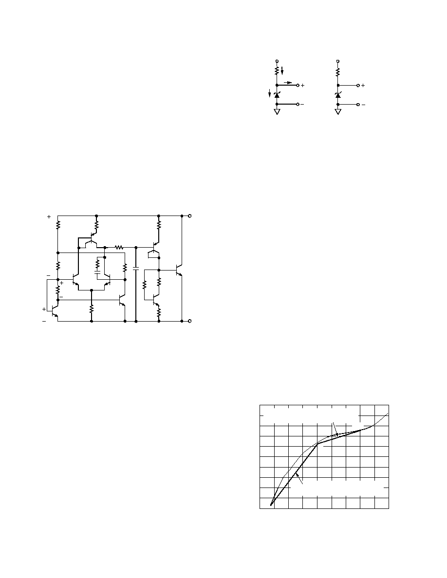
TURN-ON TIME
Many low power instrument manufacturers are becoming
increasingly concerned with the turn-on characteristics of
components being used in their systems. Fast turn-on components
often enable the end user to keep power off when not needed,
and yet respond quickly when the power is turned on for
operation. Figure 14a displays the turn-on characteristic of the
AD1580. Upon application of power (cold start), the time
required for the output voltage to reach its final value within a
specified error is the turn-on settling time. Two components
normally associated with this are: time for active circuits to
settle and time for thermal gradients on the chip to stabilize.
This characteristic is generated from cold-start operation and
represents the true turn-on waveform after power up. Figure 15
shows both the coarse and fine turn-on settling characteristics of
the device; the total settling time to within 1.0 mV is about 6 us,
and there is no long thermal tail when the horizontal scale is
expanded to 2 ms/div.
250mV/DIV
5µs/DIV
2.4V
0V
V
IN
C
L
= 200pF
Figure 14a. Response Time
V
IN
V
R
R
S
= 11.5k
R
L
C
L
V
OUT
Figure 14b. Turn-On, Settling, and Transient Test Circuit
Output turn-on time is modified when an external noise reduction
filter is used. When present, the time constant of the filter will
dominate overall settling.
OUTPUT ERROR
1mV/DIV 2 µs/DIV
2.4V
0V
V
IN
OUTPUT
0.5mV/DIV 2 ms/DIV
Figure 15. Turn-On Settling
TRANSIENT RESPONSE
Many A/D and D/A converters present transient current loads
to the reference, and poor reference response can degrade the
converter's performance.
Figure 16 displays both the coarse and fine settling characteristics
of the device to load transients of
±
50
µ
A.
I
R
= 100µA + 50µA STEP
I
R
= 100µA ≠ 50µA STEP
20mV/DIV
1mV/DIV
1µs/DIV
20mV/DIV
1mV/DIV
(a)
(b)
Figure 16. Transient Settling
Figure 16a shows the settling characteristics of the device for an
increased reverse current of 50
µ
A. Figure 16b shows the
response when the reverse current is decreased by 50
µ
A. The
transients settle to 1 mV in about 3
µ
s.
Attempts to drive a large capacitive load (in excess of 1,000 pF)
may result in ringing, as shown in the step response photo
(Figure 17). This is due to the additional poles formed by the
load capacitance and the output impedance of the reference. A
recommended method of driving capacitive loads of this magnitude
is shown in Figure 14b. A resistor isolates the capacitive load from
the output stage, while the capacitor provides a single pole low-
pass filter and lowers the output noise.
AD1580
REV. 0
≠7≠
10mV/DIV
50µs/DIV
C
L
= 0.01µF
V
IN
2.0V
1.8V
Figure 17. Transient Response with Capacitive Load
PRECISION MICROPOWER LOW DROPOUT
REFERENCE
The circuit in Figure 18 provides an ideal solution for making a
stable voltage reference with low standby power consumption,
low input/output dropout capability, and minimum noise
output. The amplifier both buffers and optionally scales up the
AD1580 output voltage, V
R
. Output voltages as high as 2.1 V
can supply 1 mA of load current. A one-pole filter connected
between the AD1580 and the OP193 input may be used to
achieve low output noise. The nominal quiescent power consump-
tion is a mere 200
µ
W.
3V
34.8k
205
4.7µF
AD1580
OP193
R3
R2
V
OUT
= +1.225 (1+R2/R3)
V
OUT
= +1.225V
OR
Figure 18. Micropower Buffered Reference
USING THE AD1580 WITH 3 V DATA CONVERTERS
The AD1580's low output drift (50 ppm/
∞
C) and compact sub-
miniature SOT-23 package makes it ideally suited for today's
high performance converters in space critical applications.
One family of ADCs that the AD1580 is well suited for is the
AD7714-3 and AD7715-3. The AD7714/AD7715 are charge-
balancing (sigma-delta) A/D converters with on-chip digital
filtering intended for the measurement of wide dynamic range,
low frequency signals such as those representing chemical,
physical or biological processes. Figure 19 shows the AD1580
connected to the AD7714/AD7715 for 3 V operation.
AD7714/15≠3
C
REF
(3≠8pF)
SWITCHING
FREQUENCY DEPENDS
ON F
CLKIN
AD1580
3V
34.8k
REFIN(+)
REFIN(≠)
R
SW
5k
(TYP)
HIGH
IMPEDANCE
>1G
Figure 19. Reference Circuit for the AD7714/AD7715≠3
The AD1580 is ideal for creating the reference level to use with
12-bit multiplying DACs such as the AD7943, AD7945, and
AD7948. In the single supply bias mode (Figure 20), the
impedance seen looking into the I
OUT2
terminal changes with
DAC code. If the AD1580 drives I
OUT2
and AGND directly,
less than 0.2 LSBs of additional linearity error will result. The
buffer amp eliminates any linearity degradation that could result
from variations in the reference level .
DAC
AD7943/45/48
V
REF
V
IN
V
DD
RBF
I
OUT1
I
OUT2
A1: OP295
AD822
OP2283
V
OUT
AGND
DGND
A1
A1
C1
+3.3V
41.2k
+3.3V
AD1580
SIGNAL GROUND
Figure 20. Single Supply System
AD1580
REV. 0
≠8≠
OUTLINE DIMENSIONS
Dimensions shown in inches and (mm).
SOT-23
0.550 (1.397)
0.0470 (1.194)
0.0413 (1.049)
0.0374 (0.950)
0.0807 (2.050)
0.0701 (1.781)
0.0236 (0.599)
0.0177 (0.450)
0.0040 (0.102)
0.0005 (0.013)
0.0210 (0.533)
0.0146 (0.371)
0.0440 (1.118)
0.0320 (0.813)
0.0100 (0.254)
0.0050 (0.127)
0.0059 (0.150)
0.0034 (0.086)
0.027 (0.686)
REF
SEATING
PLANE
PIN 1
0.1040 (2.642)
0.0827 (2.101)
0.1200 (3.048)
0.1102 (2.799)
TAPE AND REEL DIMENSIONS
Dimensions shown in millimeters.
1.5
+0.05
≠0.00
4.0
±
0.10
2.0
±
0.05
DIRECTION OF UNREELING
1.0 MIN
0.75 MIN
1.8
±
0.1
0.30
±
0.05
2.7
±
0.1
1.75
±
0.10
3.5
±
0.05
3.1
±
0.1
8.0
±
0.30
20.2 MIN
1.5 MIN
180 (7")
OR
330 (13")
14.4 MAX
8.4
+1.5
≠0.0
50 (7") MIN
OR
100 (13") MIN
13.0
±
0.2
C2081≠18≠10/95
PRINTED IN U.S.A.