
a
SoundPort Controller
AD1812
FEATURES
Compatibility with:
Sound Blaster Pro*
AdLib*
Windows* Sound System
16-Bit
Stereo Codec
MPC Level-2+ Mixer
Dual DMA/Full Duplex Operation
On-Chip FIFO Buffers
Sample Rates from 5.5 kHz to 50 kHz
ADPCM Compression/Decompression
Plug and Play Compliant
Compatible MIDI MPU-401 Port
Integrated Game Port
Free Supporting Software:
Windows 3.1 Driver
Windows 95 Driver
Control Applets
Diagnostics
Power Management Modes
Operation from +5 V Supply
16-Bit Parallel Interface to ISA Bus
24 mA Bus Drive Capability
*Sound Blaster Pro is a trademark of Creative Labs, Ltd.
*
AdLib is a trademark of AdLib Multimedia.
*
Windows is a trademark and Microsoft is a registered trademark of
*
Microsoft Corp.
SoundPort is a registered trademark of Analog Devices, Inc.
PRODUCT OVERVIEW
The AD1812 SoundPort� Controller is a single chip audio sub-
system for adding 16-bit stereo audio to personal computers.
The AD1812 is compatible with Sound Blaster Pro, AdLib, and
the Microsoft* Windows Sound System. The AD1812 provides
an integrated audio solution for enhanced business audio, enter-
tainment sound effects, and multimedia applications.
The AD1812 audio subsystem combines an integrated digital
audio controller, a powerful signal processor, a mixer, and a
16-bit
stereo codec. The DOS games register set, the Win-
dows Sound System register set, music synthesis hardware, an
MPU-401 compatible UART interface, a game port (with
timer), and a Plug and Play ISA interface are all contained on
chip. The on-chip Plug and Play (PnP) routine provides con-
figuration services for the internal logical devices and an exter-
nal modem chipset.
The AD1812 can record compress and playback voice, sound
and music. The system provides all PC 95 audio conversion and
compatibility requirements for a multimedia enabled PC.
(continued on Page 12)
FUNCTIONAL BLOCK DIAGRAM
0dB/
20dB
G
M
G
M
G
M
M
G
G
M
M
SELECTOR
D/A
CONVERTER
ATTN/
MUTE
A/D
CONVERTER
PGA
DIGITAL MIX
ATTENUATE
FORMAT
FIFO
FORMAT
FIFO
GAME
REGISTER
SET
&
WSS
REGISTER
SET
MIDI _IN
MPU-401 UART
JOYSTICK/GAME PORT INTERFACE
MIDI _OUT
A_1 B_1 A_X B_X A_2 B_2 A_Y B_Y
XTALI/O
PARALLEL
BUS
INTERFACE
CONTROL
REGISTERS
PLUG
AND
PLAY
REGISTERS
ATTN
D/A
CONVERTER
ADSP-2171
ROM
RAM
MIC
LINE
AUX1
L_OUT
MONO I/O
R_OUT
MONO_IN
AUX2
DACIN
DACOUT
DRQ (0, 1, 3, 5, 6, 7)
IRQ (3, 4, 5, 7, 9, 10, 11, 12)
PC_D (15:0)
PC_A (15:0)
AEN
DACK (0, 1, 3, 5, 6, 7)
IOR
IOW
SBHE
IO_CH16
PWRDWN
PnP
AD1812
MODEM_IRQ
MODEM_SEL
G = GAIN/AMPLIFIER BLOCK
M = MUTE BLOCK
OSCILLATORS
REV. 0
Information furnished by Analog Devices is believed to be accurate and
reliable. However, no responsibility is assumed by Analog Devices for its
use, nor for any infringements of patents or other rights of third parties
which may result from its use. No license is granted by implication or
otherwise under any patent or patent rights of Analog Devices.
� Analog Devices, Inc., 1996
One Technology Way, P.O. Box 9106, Norwood, MA 02062-9106, U.S.A.
Tel: 617/329-4700
Fax: 617/326-8703

REV. 0
�2�
AD1812�SPECIFICATIONS
STANDARD TEST CONDITIONS UNLESS OTHERWISE NOTED
DAC Test Conditions
Temperature
0
�
C
Calibrated
Digital Supply (V
DD
)
5.0
V
0 dB Attenuation
Analog Supply (V
CC
)
5.0
V
Input Full Scale
16-Bit Linear Mode
Sample Rate (F
S
)
48
kHz
10 k
Output Load
Input Signal
1008
Hz
Mute Off
Analog Output Passband
20 Hz to 20 kHz
ADC Test Conditions
V
IH
2.0
V
Calibrated
0 dB Gain
V
IL
0.8
V
Input �1.0 dB Relative to Full Scale
V
OH
2.4
V
Line Input Selected
V
OL
0.4
V
16-Bit Linear Mode
ANALOG INPUT
Parameter
Min
Typ
Max
Units
Input Voltage (RMS Values Assume Sine Wave Input)
LINE, AUX1, MONO_IN, AUX2, DACIN
1
V rms
2.55
2.83
3.11
V p-p
MIC with +20 dB Gain (MGE = 1)
0.1
V rms
0.250
0.283
0.316
V p-p
MIC with 0 dB Gain (MGE = 0)
1
V rms
2.55
2.83
3.11
V p-p
Input Impedance*
10
17
k
Input Capacitance*
15
pF
PROGRAMMABLE GAIN AMPLIFIER--ADC
Parameter
Min
Typ
Max
Units
Step Size (0 dB to 22.5 dB)
1.3
1.5
1.7
dB
(All Steps Tested)
PGA Gain Range Span
21.5
22.5
23.5
dB
AUXILIARY, LINE, MICROPHONE AND MONO INPUT ANALOG GAIN/AMPLIFIERS/ATTENUATORS
Parameter
Min
Typ
Max
Units
Step Size: AUX1, AUX2, DACIN, LINE, MIC (All Steps Tested)
(+12 dB to �30 dB)
1.25
1.5
1.75
dB
(�31.5 dB to �34.5 dB)
1
1.5
2.0
dB
Input Gain/Attenuation Range: AUX1, AUX2, DACIN, LINE, MIC
45.0
46.5
47.5
dB
Step Size: MONO_IN (All Steps Tested)
(0 dB to �39 dB)
2.5
3.0
3.6
dB
(�42 dB to �45 dB)
2.2
3.0
3.85
dB
Input Gain/Attenuation Range: MONO_IN
43
45
46
dB
DIGITAL DECIMATION AND INTERPOLATION FILTERS*
Parameter
Min
Typ
Max
Units
Passband
0
0.4
�
F
S
Hz
Passband Ripple
�
0.1
dB
Transition Band
0.4
�
F
S
0.6
�
F
S
Hz
Stopband
0.6
�
F
S
Hz
Stopband Rejection
74
dB
Group Delay
15/F
S
sec
Group Delay Variation Over Passband
0.0
�
s
*Guaranteed not tested.
Specifications subject to change without notice.

ANALOG-TO-DIGITAL CONVERTERS
Parameter
Min
Typ
Max
Units
Resolution
16
Bits
Dynamic Range (�60 dB Input THD+N Referenced to Full Scale,
80
86
dB
A-Weighted)
THD+N (Referenced to Full Scale)
0.02
%
�78
�74
dB
Signal-to-Intermodulation Distortion* (CCIF Method)
80
dB
ADC Crosstalk*
Line Inputs (Input L, Ground R, Read R; Input R, Ground L, Read L)
�90
�80
dB
Line to MIC (Input LINE, Ground and Select MIC, Read ADC)
�90
�80
dB
Line to AUX1
�90
�80
dB
Line to AUX2
�90
�80
dB
Gain Error (Full-Scale Span Relative to Nominal Input Voltage)
�
10
%
Interchannel Gain Mismatch (Difference of Gain Errors)
�
0.5
dB
ADC Offset Error
10
mV
DIGITAL-TO-ANALOG CONVERTERS
Parameter
Min
Typ
Max
Units
Resolution
16
Bits
Dynamic Range (�60 dB Input THD+N Referenced to Full Scale,
74
81
dB
A-Weighted)
THD+N (Referenced to Full Scale)
0.022
%
�77
�73
dB
Signal-to-Intermodulation Distortion* (CCIF Method)
90
dB
Gain Error (Full-Scale Span Relative to Nominal Input Voltage)
�
15
%
Interchannel Gain Mismatch (Difference of Gain Errors)
�
0.5
dB
DAC Crosstalk* (Input L, Zero R, Measure R_OUT; Input R,
�90
�80
dB
Zero L, Measure L_OUT)
Total Out-of-Band Energy (Measured from 0.6
�
F
S
to 100 kHz)*
�60
dB
Audible Out-of-Band Energy (Measured from 0.6
�
F
S
to 20 kHz)*
�70
dB
DAC ATTENUATOR
Parameter
Min
Typ
Max
Units
Step Size (0 dB to �22.5 dB)
1.3
1.5
1.7
dB
Step Size (�22.5 dB to �94.5 dB)*
1.0
1.5
2.0
dB
Output Attenuation Range Span*
93.5
94.5
95.5
dB
Mute Attenuation of 0 dB Fundamental*
80
dB
DIGITAL MIX ATTENUATOR
Parameter
Min
Typ
Max
Units
Step Size (0 dB to �22.5 dB)
1.3
1.5
1.7
dB
Step Size (�22.5 dB to �94.5 dB)*
1.0
1.5
2.0
dB
Digital Mix Attenuation Range Span*
93.5
94.5
95.5
dB
*Guaranteed not tested.
Specifications subject to change without notice.
AD1812
REV. 0
�3�

AD1812
REV. 0
�4�
ANALOG OUTPUT
Parameter
Min
Typ
Max
Units
Full-Scale Output Voltage
O
L
= 0
1.8
2.0
2.2
V p-p
O
L
= 1
2.5
2.8
3.11
V p-p
Output Impedance*
600
External Load Impedance
10
k
Output Capacitance*
15
pF
External Load Capacitance
100
pF
V
REF
2.05
2.25
2.45
V
V
REF
Output Impedance
4
k
Mute Click (Muted Output Minus Unmuted Midscale DAC Output)*
�
5
mV
SYSTEM SPECIFICATIONS
Parameter
Min
Typ
Max
Units
System Frequency Response Ripple* (Line In to Line Out)
1.0
dB
Differential Nonlinearity*
�
1
LSB
Phase Linearity Deviation*
5
Degrees
STATIC DIGITAL SPECIFICATIONS
Parameter
Min
Typ
Max
Units
High-Level Input Voltage (V
IH
): Digital Inputs
2
V
Low-Level Input Voltage (V
IL
)
0.8
V
High-Level Output Voltage (V
OH
), I
OH
= 24 mA
2.4
V
Low-Level Output Voltage (V
OL
), I
OL
= 24 mA
0.4
V
Input Leakage Current
�10
10
�
A
Output Leakage Current
�10
10
�
A
POWER SUPPLY
Parameter
Min
Typ
Max
Units
Power Supply Range--Analog
4.75
5.25
V
Power Supply Range--Digital
4.75
5.25
V
Power Supply Current
250
mA
Power Dissipation
1.25
W
Analog Supply Current
55
mA
Digital Supply Current
195
mA
Digital Power Supply Current--Power Down
15
mA
Analog Power Supply Current--Power Down
1
mA
Power Supply Rejection (100 mV p-p Signal @ 1 kHz)*
(At Both Analog and Digital Supply Pins, Both ADCs and DACs)
40
dB
CLOCK SPECIFICATIONS*
Parameter
Min
Typ
Max
Units
Input Clock Frequency
6
14.31818
18
MHz
Recommended Clock Duty Cycle
10
50
90
%
Power Up Initialization Time
500
ms
*Guaranteed not tested.
Specifications subject to change without notice.
AD1812
REV. 0
�5�
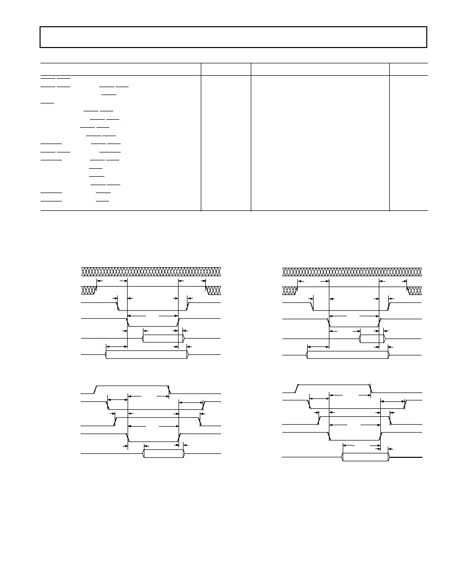
TIMING PARAMETERS (GUARANTEED OVER OPERATING TEMPERATURE RANGE)
Parameter
Symbol
Min
Typ
Max
Units
IOW
/IOR Strobe Width
t
STW
100
ns
IOW
/IOR Rising to IOW/IOR Falling
t
BWDN
80
ns
Write Data Setup to IOW Rising
t
WDSU
10
ns
IOR
Falling to Valid Read Data
t
RDDV
40
ns
AEN Setup to IOW/IOR Falling
t
AESU
10
ns
AEN Hold from IOW/IOR Rising
t
AEHD
0
ns
Adr Setup to IOW/IOR Falling
t
ADSU
10
ns
Adr Hold from IOW/IOR Rising
t
ADHD
10
ns
DACK
Rising to IOW/IOR Falling
t
DKSU1
20
ns
IOW
/IOR Rising to DACK Falling
t
DKHD1
0
ns
DACK
Setup to IOW/IOR Falling
t
DKSU2
10
ns
Data Hold from IOR Rising
t
DHD1
20
ns
Data Hold from IOW Rising
t
DHD2
15
ns
DRQ Hold from IOW/IOR Falling
t
DRHD
25
ns
DACK
Hold from IOW Rising
t
DKHD2
10
ns
DACK
Hold from IOR Rising
t
DKHD3
10
ns
*Guaranteed, not tested.
Specifications subject to change without notice.
General Notes
Use the exact timing information given. Do not attempt to derive parameters from the addition or subtraction of others. While addition or subtraction would yield
meaningful results for an additional device, the values given in this data sheet reflect statistical variations and worst cases. Consequently, you cannot meaningfully add
up parameters to derive longer times. Note that all 8-bit DMA transfers occur on channels 0, 1, and 3, while all 16-bit DMA transfers occur on channels 5, 6, and 7.
t
DKSU1
t
DKHD1
t
AESU
t
AEHD
t
STW
t
RDDV
t
DHD1
t
ADHD
t
ADSU
DRQ
(0, 1, 3, 5, 6, 7)
DACK
(0, 1, 3, 5, 6, 7)
AEN
IOR
PC_D (7:0) /
PC_D (15:0)
PC_A (15:0)
Figure 1. PIO Read Cycle
t
DKHD3
t
AESU
t
AEHD
t
RDDV
t
DHD1
t
DKSU2
t
DRHD
DRQ
(0, 1, 3, 5, 6, 7)
DACK
(0, 1, 3, 5, 6, 7)
AEN
IOR
PC_D (7:0) /
PC_D (15:0)
t
STW
Figure 3. DMA Read Cycle
t
DKSU1
t
DKHD1
t
AESU
t
AEHD
t
STW
t
DHD2
t
ADHD
DRQ
(0, 1, 3, 5, 6, 7)
DACK
(0, 1, 3, 5, 6, 7)
AEN
IOW
PC_D (7:0) /
PC_D (15:0)
PC_A (15:0)
t
ADSU
t
WDSU
Figure 2. PIO Write Cycle
t
DKHD2
t
AESU
t
AEHD
t
DHD2
t
DKSU2
t
DRHD
DRQ
(0, 1, 3, 5, 6, 7)
DACK
(0, 1, 3, 5, 6, 7)
AEN
IOW
PC_D (7:0) /
PC_D (15:0)
t
STW
t
WDSU
Figure 4. DMA Write Cycle