 | –≠–ª–µ–∫—Ç—Ä–æ–Ω–Ω—ã–π –∫–æ–º–ø–æ–Ω–µ–Ω—Ç: AD1819A | –°–∫–∞—á–∞—Ç—å:  PDF PDF  ZIP ZIP |
REV. 0
Information furnished by Analog Devices is believed to be accurate and
reliable. However, no responsibility is assumed by Analog Devices for its
use, nor for any infringements of patents or other rights of third parties
which may result from its use. No license is granted by implication or
otherwise under any patent or patent rights of Analog Devices.
a
AD1819A
One Technology Way, P.O. Box 9106, Norwood, MA 02062-9106, U.S.A.
Tel: 781/329-4700
World Wide Web Site: http://www.analog.com
Fax: 781/326-8703
© Analog Devices, Inc., 1998
AC '97 SoundPort
Æ
Codec
AC '97 FEATURES
Fully Compliant AC '97 Analog I/O Component
48-Terminal TQFP Package
Multibit
Converter Architecture for Improved
S/N Ratio >90 dB
16-Bit Stereo Full-Duplex Codec
Four Analog Line-Level Stereo Inputs for Connection
from LINE, CD, VIDEO and AUX
Two Analog Line-Level Mono Inputs for Speakerphone
and PC BEEP
Mono MIC Input Switchable from Two External
Sources
High Quality CD Input with Ground Sense
Stereo Line Level Output
Mono Output for Speakerphone
Power Management Support
ENHANCED FEATURES
Support for Multiple Codec Communications
DSP 16-Bit Serial Port Format
Variable 7 kHz to 48 kHz Sampling Rate with 1 Hz
Resolution
Supports Modem Sample Rates and Filtering
PhatTM Stereo 3D Stereo Enhancement
VHDL and Verilog Models of Serial Port Available
SoundPort is a registered trademark of Analog Devices, Inc.
Phat is a trademark of Analog Devices, Inc.
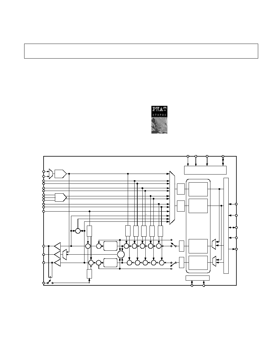
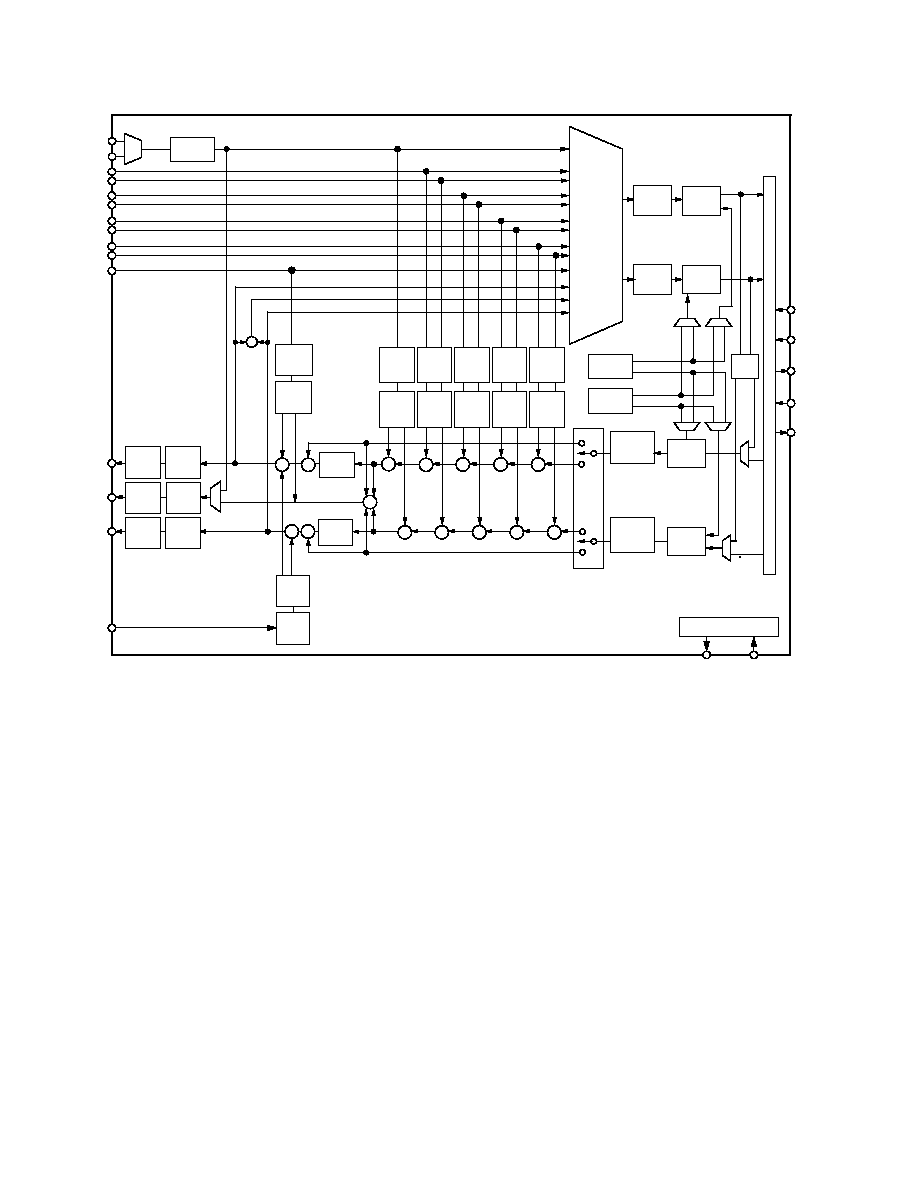
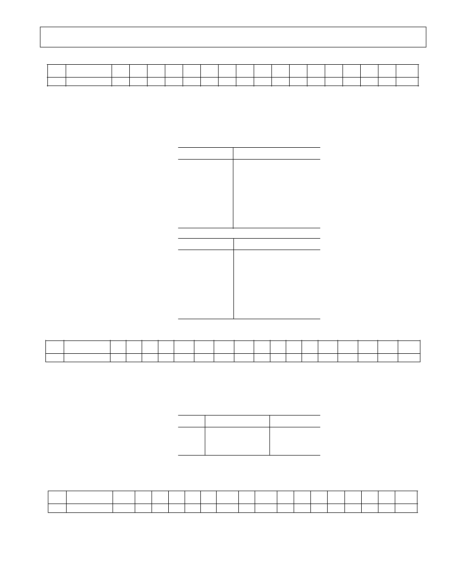
FUNCTIONAL BLOCK DIAGRAM
G
A
M
G
A
M
G
A
M
AC LINK
SYNC
BIT_CLK
PHAT
STEREO
PHAT
STEREO
G
A
M
A
M
MV
0dB/
20dB
MV
AD1819A
MIC1
MIC2
AUX
CD
VIDEO
PC_BEEP
LINE_OUT_L
MONO_OUT
LINE_IN
PHONE_IN
LINE_OUT_R
MV
SELECTOR
PGA
PGA
16-BIT
A/D
CONVERTER
G
A
M
SAMPLE
RATE
GENERATORS
G = GAIN
A = ATTENUATE
M = MUTE
MV = MASTER VOLUME
OSCILLATORS
XTALO
XTALI
CS1 CHAIN_IN
CHAIN_CLK
RESET
SDATA_IN
CS0
MASTER/SLAVE
SYNCHRONIZER
SDATA_OUT
G
A
M
16-BIT
A/D
CONVERTER
G
A
M
G
A
M
16-BIT
D/A
CONVERTER
16-BIT
D/A
CONVERTER

AD1819A
≠2≠
REV. 0
PRODUCT OVERVIEW
The AD1819A SoundPort Codec is designed to meet all require-
ments of the Audio Codec '97, Component Specification, Revision
1.03, © 1996, Intel Corporation, found at www.Intel.com. In
addition, the AD1819A supports multiple codec configurations
(up to three per AC-Link), a DSP serial mode, variable sample
rates, modem sample rates and filtering, and built-in Phat Ste-
reo 3D enhancement.
The AD1819A is an analog front end for high performance PC
audio, modem, or DSP applications. The AC '97 architecture
defines a 2-chip audio solution comprising a digital audio con-
troller, plus a high quality analog component that includes
Digital-to-Analog Converters (DACs), Analog-to-Digital Con-
verters (ADCs) mixer and I/O.
The main architectural features of the AD1819A are the high
quality analog mixer section, two channels of
ADC conver-
sion, two channels of
DAC conversion and Data Direct
Scrambling (D
2
S) rate generators. The AD1819A's left channel
ADC and DAC are compatible for modem applications support-
ing irrational sample rates and modem filtering requirements.
FUNCTIONAL DESCRIPTION
This section overviews the functionality of the AD1819A and is
intended as a general introduction to the capabilities of the
device. Detailed reference information may be found in the
descriptions of the Indexed Control Registers.
Analog Inputs
The codec contains a stereo pair of
ADCs. Inputs to the
ADC may be selected from the following analog signals: tele-
phony (PHONE_IN), mono microphone (MIC1 or MIC2),
stereo line (LINE_IN), auxiliary line input (AUX), stereo CD
ROM (CD), stereo audio from a video source (VIDEO) and
post-mixed stereo or mono line output (LINE_OUT).
Analog Mixing
PHONE_IN, MIC1 or MIC2, LINE_IN, AUX, CD and
VIDEO can be mixed in the analog domain with the stereo
output from the DACs. Each channel of the stereo analog in-
puts may be independently gained or attenuated from +12 dB
to ≠34.5 dB in 1.5 dB steps. The summing path for the mono
inputs (PHONE_IN, MIC1, and MIC2 to LINE_OUT) dupli-
cates mono channel data on both the left and right LINE_OUT.
Additionally, the PC attention signal (PC_BEEP) may be
mixed with the line output. A switch allows the output of the
DACs to bypass the Phat Stereo 3D enhancement.
Analog-to-Digital Signal Path
The selector sends left and right channel signals to the program-
mable gain amplifier (PGA). The PGA following the selector
allows independent gain for each channel entering the ADC
from 0 dB to +22.5 dB in 1.5 dB steps.
Each channel of the ADC is independent, and can process
left and right channel data at different sample rates. All pro-
grammed sample rates from 7 kHz to 48 kHz have a resolution
of 1 Hz. The AD1819A also supports irrational V.34 sample
rates.
Sample Rates and D
2
S
The AD1819A default mode sets the codec to operate at 48 kHz
sample rates. The converter pairs may process left and right
channel data at different sample rates. The AD1819A sample
rate generator allows the codec to instantaneously change and
process sample rates from 7 kHz to 48 kHz with a resolution of
1 Hz. The in-band integrated noise and distortion artifacts in-
troduced by rate conversions are below ≠90 dB. The AD1819A
uses a 4-bit D/A structure and Data Directed Scrambling (D
2
S)
to enhance noise immunity on motherboards and in PC enclo-
sures, and to suppress idle tones below the device's quantization
noise floor. The D
2
S process pushes noise and distortion arti-
facts caused by errors in the multibit D/A conversion process to
frequencies beyond the audible range of the human ear and then
filters them.
Digital-to-Analog Signal Path
The analog output of the DAC may be gained or attenuated
from +12 dB to ≠34.5 dB in 1.5 dB steps, and summed with any
of the analog input signals. The summed analog signal enters
the Master Volume stage where each channel of the mixer out-
put may be attenuated from 0 dB to ≠46.5 dB in 1.5 dB steps or
muted.
Host-Based Echo Cancellation Support
The AD1819A supports time correlated I/O data format by
presenting mic data on the left channel of the ADC and the
mono summation of left and right output on the right channel.
The ADC is splittable; left and right ADC data can be sampled
at different rates.
Telephony Modem Support
The AD1819A contains a V.34-capable analog front end for
supporting host-based and data pump modems. The modem
DAC typical dynamic range is 90 dB over a 4.2 kHz analog
output passband where F
S
= 12.8 kHz. The left channel of the
ADC and DAC may be used to convert modem data at the same
sample rate in the range between 7 kHz and 48 kHz. All pro-
grammed sample rates have a resolution of 1 Hz. The AD1819A
supports irrational V.34 sample rates with 8/7 and 10/7 select-
able sample rate multiplier coefficients.

≠3≠
REV. 0
AD1819A
STANDARD TEST CONDITIONS UNLESS OTHERWISE NOTED
DAC Test Conditions
Temperature
25
∞
C
Calibrated
Digital Supply (V
DD
)
5.0
V
0 dB Attenuation
Analog Supply (V
CC
)
5.0
V
Input 0 dB
Sample Rate (F
S
)
48
kHz
10 k
Output Load
Input Signal
1008
Hz
Mute Off
Analog Output Passband
20 Hz to 20 kHz
ADC Test Conditions
V
IH
(AC-Link)
2.0
V
Calibrated
V
IL
(AC-Link)
0.8
V
0 dB Gain
V
IH
(CS0, CS1, CHAIN_IN)
4.0
V
Input ≠3 dB Relative to Full Scale
V
IL
(CHAIN_CLK)
1.0
V
Line Input Selected
ANALOG INPUT
Parameter
Min
Typ
Max
Units
Input Voltage (RMS Values Assume Sine Wave Input)
LINE_IN, AUX, CD, VIDEO, PHONE_IN, PC_BEEP
1
V rms
2.83
V p-p
MIC1, MIC2 with +20 dB Gain (M20 = 1)
0.1
V rms
0.283
V p-p
MIC1, MIC2 with 0 dB Gain (M20 = 0)
1
V rms
2.83
V p-p
Input Impedance*
10
k
Input Capacitance*
15
pF
PROGRAMMABLE GAIN AMPLIFIER--ADC
Parameter
Min
Typ
Max
Units
Step Size (0 dB to 22.5 dB)
1.5
dB
PGA Gain Range Span
22.5
dB
ANALOG MIXER-- INPUT GAIN/AMPLIFIERS/ATTENUATORS
Parameter
Min
Typ
Max
Units
Dynamic Range (≠60 dB Input THD+N, Referenced to Full Scale, A-Weighted)
CD to LINE_OUT
90
dB
Other to LINE_OUT*
90
dB
Step Size (+12 dB to ≠34.5 dB): (All Steps Tested)
MIC, LINE_IN, AUX, CD, VIDEO, PHONE_IN, DAC
1.5
dB
Input Gain/Attenuation Range
MIC, LINE_IN, AUX, CD, VIDEO, PHONE_IN, DAC
46.5
dB
Step Size (0 dB to ≠45 dB): (All Steps Tested)
PC_BEEP
3.0
dB
Input Gain/Attenuation Range: PC_BEEP
45
dB
DIGITAL DECIMATION AND INTERPOLATION FILTERS*
Parameter
Min
Typ
Max
Units
Passband
0
0.4
◊
F
S
Hz
Passband Ripple
±
0.09
dB
Transition Band
0.4
◊
F
S
0.6
◊
F
S
Hz
Stopband
0.6
◊
F
S
Hz
Stopband Rejection
≠74
dB
Group Delay
12/F
S
sec
Group Delay Variation Over Passband
0.0
µ
s
*Guaranteed, not tested.
Specifications subject to change without notice.
SPECIFICATIONS

≠4≠
REV. 0
AD1819A≠SPECIFICATIONS
ANALOG-TO-DIGITAL CONVERTERS
Parameter
Min
Typ
Max
Units
Resolution
16
Bits
Total Harmonic Distortion (THD)
0.02
%
≠74
dB
Dynamic Range (≠60 dB Input THD+N Referenced to Full Scale,
A-Weighted)
84
87
dB
Signal-to-Intermodulation Distortion* (CCIF Method)
85
dB
ADC Crosstalk*
Line Inputs (Input L, Ground R, Read R; Input R, Ground L, Read L)
≠100
≠90
dB
Line to Other
≠90
≠85
dB
Gain Error (Full-Scale Span Relative to Nominal Input Voltage)
±
10
%
Interchannel Gain Mismatch (Difference of Gain Errors)
±
0.5
dB
ADC Offset Error
±
5
mV
DIGITAL-TO-ANALOG CONVERTERS
Parameter
Min
Typ
Max
Units
Resolution
16
Bits
Total Harmonic Distortion (THD) LINE_OUT
0.02
%
≠74
dB
Dynamic Range (≠60 dB Input THD+N Referenced to Full Scale,
A-Weighted)
85
90
dB
Signal-to-Intermodulation Distortion* (CCIF Method)
85
dB
Gain Error (Full-Scale Span Relative to Nominal Input Voltage)
±
10
%
Interchannel Gain Mismatch (Difference of Gain Errors)
±
0.5
dB
DAC Crosstalk* (Input L, Zero R, Measure LINE_OUT_R; Input R,
dB
Zero L, Measure LINE_OUT_L)
≠80
dB
Total Out-of-Band Energy (Measured from 0.6
◊
F
S
to 20 kHz)*
≠40
dB
MASTER VOLUME
Parameter
Min
Typ
Max
Units
Step Size (0 dB to ≠46.5 dB)
LINE_OUT_L, LINE_OUT_R, MONO_OUT
1.5
dB
Output Attenuation Range Span
46.5
dB
Mute Attenuation of 0 dB Fundamental*
75
dB
ANALOG OUTPUT
Parameter
Min
Typ
Max
Units
Full-Scale Output Voltage
1
V rms
2.83
V p-p
Output Impedance*
800
External Load Impedance
10
k
Output Capacitance*
15
pF
External Load Capacitance
100
pF
V
REF
2.00
2.25
2.50
V
V
REF
Current Drive
100
µ
A
V
REFOUT
2.25
V
V
REFOUT
Current Drive
5
mA
Mute Click (Muted Output Minus Unmuted Midscale DAC Output)*
±
5
mV
*Guaranteed, not tested.
Specifications subject to change without notice.

STATIC DIGITAL SPECIFICATIONS
Parameter
Min
Typ
Max
Units
High-Level Input Voltage (V
IH
): Digital Inputs
0.4
◊
DV
DD
V
Low-Level Input Voltage (V
IL
)
0.2
◊
DV
DD
V
High-Level Output Voltage (V
OH
), I
OH
= 2 mA
0.5
◊
DV
DD
V
Low-Level Output Voltage (V
OL
), I
OL
= 2 mA
0.2
◊
DV
DD
V
Input Leakage Current
≠10
10
µ
A
Output Leakage Current
≠10
10
µ
A
POWER SUPPLY
Parameter
Min
Typ
Max
Units
Power Supply Range--Analog
4.5
5.5
V
Power Supply Range--Digital
4.5
5.5
V
Power Supply Current
120
mA
Power Dissipation
600
mW
Analog Supply Current
60
mA
Digital Supply Current
60
mA
Power Supply Rejection (100 mV p-p Signal @ 1 kHz)*
(At Both Analog and Digital Supply Pins, Both ADCs and DACs)
≠40
dB
CLOCK SPECIFICATIONS*
Parameter
Min
Typ
Max
Units
Input Clock Frequency
24.576
MHz
Recommended Clock Duty Cycle
40
50
60
%
POWER-DOWN STATES
Parameter
Set Bits
Min
Typ
Max
Units
ADCs and Input Mux Power-Down
PR0
110
mA
DACs Power-Down
PR1
100
mA
Analog Mixer Power-Down (V
REF
and V
REFOUT
On)
PR1, PR2
54
mA
Analog Mixer Power-Down (V
REF
and V
REFOUT
Off)
PR0, PR1, PR3
47
mA
Digital Interface Power-Down*
PR4
120
mA
Internal Clocks Disabled*
PR0, PR1, PR4, PR5
85
mA
ADC and DAC Power-Down
PR0, PR1
85
mA
V
REF
Standby Mode*
PR0, PR1, PR2, PR4, PR5
55
mA
Total Power-Down
PR0, PR1, PR2, PR3,
PR4, PR5
220
µ
A
RESET (Low)
250
µ
A
*Guaranteed, not tested.
Specifications subject to change without notice.
≠5≠
REV. 0
AD1819A
AD1819A
≠6≠
REV. 0
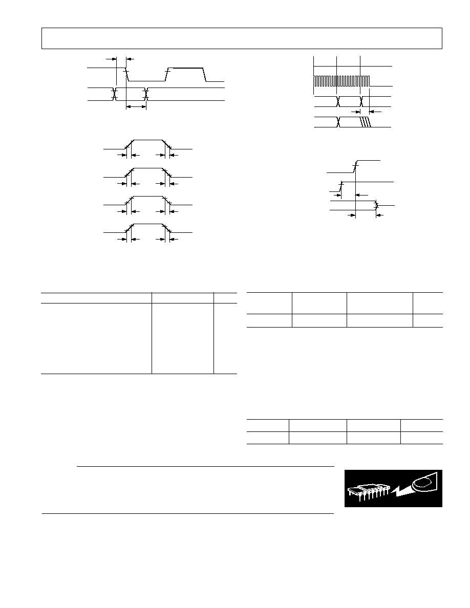
TIMING PARAMETERS (GUARANTEED OVER OPERATING TEMPERATURE RANGE)
Parameter
Symbol
Min
Typ
Max
Units
RESET Active Low Pulsewidth
t
RST_LOW
1.0
µ
s
RESET Inactive to BIT_CLK Start-Up Delay
t
RST2CLK
162.8
ns
SYNC Active High Pulsewidth
t
SYNC_HIGH
0.0814
1.3
µ
s
SYNC Low Pulsewidth
t
SYNC_LOW
19.5
µ
s
SYNC Inactive to BIT_CLK Start-Up Delay
t
SYNC2CLK
162.8
ns
BIT_CLK Frequency
12.288
MHz
BIT_CLK Period
t
CLK_PERIOD
81.4
ns
BIT_CLK Output Jitter*
750
ps
BIT_CLK High Pulsewidth
t
CLK_HIGH
32.56
40.7
48.84
ns
BIT_CLK Low Pulsewidth
t
CLK_LOW
32.56
40.7
48.84
ns
SYNC Frequency
48.0
kHz
SYNC Period
t
SYNC_PERIOD
20.8
µ
s
Setup to Falling Edge of BIT_CLK
t
SETUP
15.0
ns
Hold from Falling Edge of BIT_CLK
t
HOLD
15.0
ns
BIT_CLK Rise Time
t
RISE CLK
4
ns
BIT_CLK Fall Time
t
FALL CLK
4
ns
SYNC Rise Time
t
RISE SYNC
4
ns
SYNC Fall Time
t
FALL SYNC
4
ns
SDATA_IN Rise Time
t
RISE DIN
4
ns
SDATA_IN Fall Time
t
FALL DIN
4
ns
SDATA_OUT Rise Time
t
RISE DOUT
4
ns
SDATA_OUT Fall Time
t
FALL DOUT
4
ns
End of Slot 2 to BIT_CLK, SDATA_IN Low
t
S2_PDOWN
1.0
µ
s
Setup to Trailing Edge of RESET (Applies to
SYNC, SDATA_OUT)
t
SETUP2RST
15
ns
Rising Edge of
RESET to HI-Z Delay
t
OFF
25
ns
*Output Jitter is directly dependent on crystal input jitter.
RESET
BIT_CLK
t
RST2CLK
t
RST_LOW
Figure 1. Cold Reset
SYNC
BIT_CLK
t
SYNC_HIGH
t
RST2CLK
Figure 2. Warm Reset
t
CLK_HIGH
BIT_CLK
t
CLK_LOW
SYNC
t
SYNC_HIGH
t
SYNC_LOW
t
SYNC_PERIOD
t
CLK_PERIOD
Figure 3. Clock Timing
AD1819A
≠7≠
REV. 0
CAUTION
ESD (electrostatic discharge) sensitive device. Electrostatic charges as high as 4000 V readily
accumulate on the human body and test equipment and can discharge without detection.
Although the AD1819A features proprietary ESD protection circuitry, permanent damage may
occur on devices subjected to high energy electrostatic discharges. Therefore, proper ESD
precautions are recommended to avoid performance degradation or loss of functionality.
ABSOLUTE MAXIMUM RATINGS*
Parameter
Min
Max
Units
Power Supplies
Analog (AV
DD
)
≠0.3
6.0
V
Digital (DV
DD
)
≠0.3
6.0
V
Input Current (Except Supply Pins)
±
10.0
mA
Analog Input Voltage (Signal Pins)
≠0.3
AV
DD
+ 0.3 V
Digital Input Voltage (Signal Pins)
≠0.3
DV
DD
+ 0.3 V
Ambient Temperature (Operating)
≠40
+85
∞
C
Storage Temperature
≠65
+150
∞
C
*Stresses greater than those listed under Absolute Maximum Ratings may cause
permanent damage to the device. This is a stress rating only; functional operation
of the device at these or any other conditions above those indicated in the
operational section of this specification is not implied. Exposure to absolute
maximum rating conditions for extended periods may affect device reliability.
ORDERING GUIDE
Temperature
Package
Package
Model
Range
Description
Option*
AD1819AJST ≠40
∞
C to +85
∞
C 48-Terminal TQFP ST-48
*ST = Thin Quad Flatpack.
ENVIRONMENTAL CONDITIONS
Ambient Temperature Rating
T
AMB
= T
CASE
≠ (P
D
◊
CA
)
T
CASE
= Case Temperature in
∞
C
P
D
= Power Dissipation in W
CA
= Thermal Resistance (Case-to-Ambient)
JA
= Thermal Resistance (Junction-to-Ambient)
JC
= Thermal Resistance (Junction-to-Case)
Package
JA
JC
CA
TQFP
76.2
∞
C/W
17
∞
C/W
59.2
∞
C/W
BIT_CLK
SYNC
t
HOLD
SDATA_OUT
t
SETUP
Figure 4. Data Setup and Hold
BIT_CLK
SYNC
SDATA_IN
t
RISECLK
t
RISESYNC
t
RISEDIN
t
RISEDOUT
t
FALLCLK
t
FALLSYNC
t
FALLDIN
t
FALLDOUT
SDATA_OUT
Figure 5. Signal Rise and Fall Time
BIT_CLK
SDATA_OUT
SYNC
SDATA_IN
SLOT 1
SLOT 2
WRITE
TO 0x26
DATA
PR4
DON'T
CARE
t
S2_PDOWN
NOTE: BIT_CLK NOT TO SCALE
Figure 6. AC-Link, Link Low Power Mode Timing
RESET
SDATA_OUT
HI-Z
t
SETUP2RST
t
OFF
SDATA_IN, BIT_CLK
Figure 7. ATE Test Mode
WARNING!
ESD SENSITIVE DEVICE
AD1819A
≠8≠
REV. 0
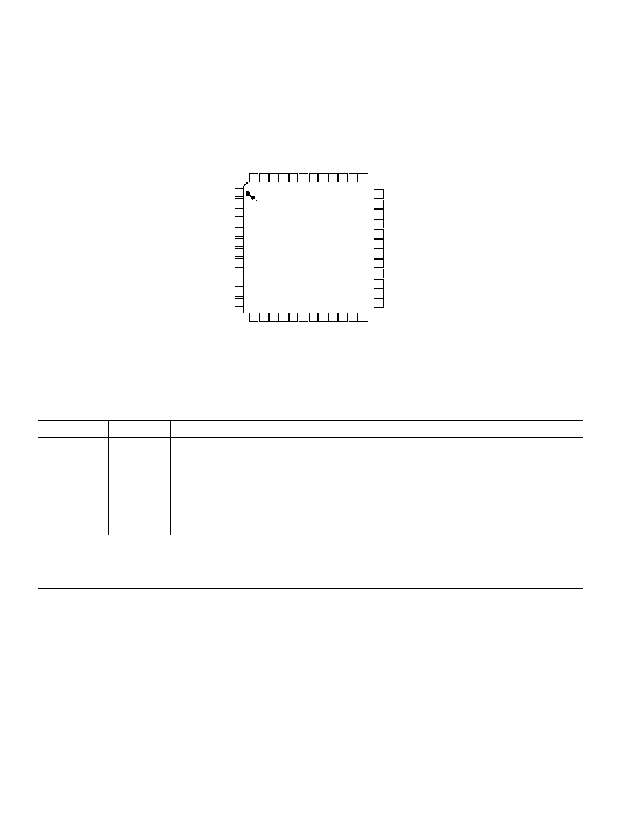
PIN CONFIGURATION
48-Terminal TQFP
(ST-48)
36
35
34
33
32
31
30
29
28
27
26
25
13 14 15 16 17 18 19 20 21 22 23 24
AV
SS2
CHAIN_IN
NC
CS0
NC
NC
NC
NC
1
2
3
4
5
6
7
8
9
10
11
12
48 47 46 45 44
39 38 37
43 42 41 40
PIN 1
IDENTIFIER
TOP VIEW
(Not to Scale)
LINE_OUT_R
LINE_OUT_L
CX3D
RX3D
FILT_L
FILT_R
AFILT2
PHONE_IN
AUX_L
AUX_R
VIDEO_L
CD_GND
DV
DD1
XTL_IN
XTL_OUT
SDATA_OUT
BIT_CLK
SDATA_IN
SYNC
RESET
PC_BEEP
NC = NO CONNECT
AFILT1
CD_R
MIC1
MIC2
LINE_IN_L
MONO_OUT
AD1819A
LINE_IN_R
CS1
CD_L
VIDEO_R
CHAIN_CLK
DV
SS1
DV
SS2
DV
DD2
V
REFOUT
V
REF
AV
SS1
AV
DD1
AV
DD2
PIN FUNCTION DESCRIPTIONS
Digital I/O
Pin Name
TQFP
I/O
Description
XTL_IN
2
I
24.576 MHz Crystal or Clock Input
XTL_OUT
3
O
24.576 MHz Crystal Output
SDATA_OUT
5
I
Serial Data Output. Serial, Time Division Multiplexed, AD1819A Input Stream
BIT_CLK
6
O/I*
Bit Clock Input, 12.288 MHz Serial Data Clock. Daisy Chain Output Clock
SDATA_IN
8
O
Serial Data Input. Serial, Time Division Multiplexed, AD1819A Output Stream
SYNC
10
I
48 kHz Fixed Rate Sample Sync Clock
RESET
11
I
Reset. AC-Link Master Hardware Reset
*Input if the AD1819A is configured as Slave 1 or Slave 2.
Daisy Chain Connections
Pin Name
TQFP
I/O
Description
CS0
45
I
Daisy Chain Codec Select
CS1
46
I
Daisy Chain Codec Select
CHAIN_IN
47
I
Daisy Chain Data Input
CHAIN_CLK
48
I/O*
24.576 MHz Buffered Clock Input/Output
*Output when configured as Master. Input when configured as Slave 1 or Slave 2.

AD1819A
≠9≠
REV. 0
Analog I/O
These signals connect the AD1819A component to analog sources and sinks, including microphones and speakers.
Pin Name
TQFP
I/O
Description
PC_BEEP
12
I
PC Beep. PC Speaker Beep Pass-Through
PHONE_IN
13
I
Phone. From Telephony Subsystem Speakerphone or Handset
AUX_L
14
I
Auxiliary Input Left Channel
AUX_R
15
I
Auxiliary Input Right Channel
VIDEO_L
16
I
Video Audio Left Channel
VIDEO_R
17
I
Video Audio Right Channel
CD_L
18
I
CD Audio Left Channel
CD_GND
19
I
CD Audio Analog Ground Sense for Differential CD Input
CD_R
20
I
CD Audio Right Channel
MIC1
21
I
Microphone 1. Desktop Microphone Input
MIC2
22
I
Microphone 2. Second Microphone Input
LINE_IN_L
23
I
Line In Left Channel
LINE_IN_R
24
I
Line In Right Channel
LINE_OUT_L
35
O
Line Out Left Channel
LINE_OUT_R
36
O
Line Out Right Channel
MONO_OUT
37
O
Monaural Output to Telephony Subsystem Speakerphone
Filter/Reference
Pin Name
TQFP
I/O
Description
V
REF
27
O
Voltage Reference Filter
V
REFOUT
28
O
Voltage Reference Output 5 mA Drive (Intended for Mic Bias)
AFILT1
29
O
Antialiasing Filter Capacitor--ADC Right Channel
AFILT2
30
O
Antialiasing Filter Capacitor--ADC Left Channel
FILT_R
31
O
AC-Coupling Filter Capacitor--ADC Right Channel
FILT_L
32
O
AC-Coupling Filter Capacitor--ADC Left Channel
RX3D
33
O
3D Phat Stereo Enhancement--Resistor
CX3D
34
I
3D Phat Stereo Enhancement--Capacitor
Power and Ground Signals
Pin Name
TQFP
I/O
Description
DV
DD1
1
I
Digital V
DD
--5.0 V
DV
SS1
4
I
Digital GND
DV
SS2
7
I
Digital GND
DV
DD2
9
I
Digital V
DD
--5.0 V
AV
DD1
25
I
Analog V
DD
--5.0 V
AV
SS1
26
I
Analog GND
AV
DD2
38
I
Analog V
DD
--5.0 V
AV
SS2
42
I
Analog GND
No Connects
Pin Name
TQFP
I/O
Description
NC
39
No Connect
NC
40
No Connect
NC
41
No Connect
NC
43
No Connect
NC
44
No Connect
AD1819A
≠10≠
REV. 0
M 0x02
MM
MMM
M 0x06
0
X
74
OSCILLATORS
XTL_OUT
XTL_IN
GAM 0x18
LOV
OM
G = GAIN
A = ATTENUATE
M = MUTE
MV = MASTER VOLUME
MIC1
MIC2
AUX
CD
VIDEO
PHONE_IN
MONO_OUT
PC_BEEP
LINE_IN
M 0x0C
PHM
GA 0x0C
PHV
M 0x0A
PCM
GA 0x0A
PCV
GM 0x1C
RIM
IM
GM 0x1C
LIM
IM
LS/RS (0)
LS (4)
RS (4)
LS (3)
RS (3)
LS (1)
RS (1)
LS/RS (6)
RS (5)
LS (2)
RS (2)
0x1A
S
E
L
E
C
T
O
R
LS/RS (7)
LS (5)
0dB/20dB
M20 0x0E
0x20
0x20
POP
M 0x14
VM
M 0x12
CM
M 0x16
AM
M 0x10
LM
M 0x0E
MCM
MIX 0x20
GM 0
X
1C
RIM
IM
STEREO MIX (L)
MONO MIX
STEREO MIX (R)
3D 0x22
DP
RESET
SYNC
BIT_CLK
SDATA_OUT
SDATA_IN
LINE_OUT_L
LINE_OUT_R
M 0x02
MM
ROV
OM
GAM 0x18
16-BIT
DAC
3D 0x22
DP
16-BIT
DAC
AC LINK
SR1 0x7A
16-BIT
ADC
16-BIT
ADC
GM 0
X
1C
LIM
IM
SR0 0x78
LPBK
0x20
GA 0x14
LVV
RVV
GA 0x12
LCV
RCV
GA 0x16
LAV
RAV
GA 0x10
LLV
RLA
GA 0x0E
MCV
0
1
A 0x06
MMV
A 0x02
RMV
A 0x02
LMV
MS
Figure 8. Block Diagram Register Map

AD1819A
≠11≠
REV. 0
Indexed Control Registers
g
e
R
m
u
N
e
m
a
N
5
1
D
4
1
D
3
1
D
2
1
D
1
1
D
0
1
D
9
D
8
D
7
D
6
D
5
D
4
D
3
D
2
D
1
D
0
D
t
l
u
a
f
e
D
h
0
0
t
e
s
e
R
X
4
E
S
3
E
S
2
E
S
1
E
S
0
E
S
9
D
I
8
D
I
7
D
I
6
D
I
5
D
I
4
D
I
3
D
I
2
D
I
1
D
I
0
D
I
h
0
0
4
0
h
2
0
e
m
u
l
o
V
r
e
t
s
a
M
M
M
X
5
V
M
L
4
V
M
L
3
V
M
L
2
V
M
L
1
V
M
L
0
V
M
L
X
X
5
V
M
R
4
V
M
R
3
V
M
R
2
V
M
R
1
V
M
R
0
V
M
R
h
0
0
0
8
h
4
0
d
e
v
r
e
s
e
R
X
X
X
X
X
X
X
X
X
X
X
X
X
X
X
X
X
h
6
0
o
n
o
M
e
m
u
l
o
V
r
e
t
s
a
M
M
M
M
X
X
X
X
X
X
X
X
X
5
V
M
M
4
V
M
M
2
V
M
M
2
V
M
M
1
V
M
M
0
V
M
M
h
0
0
0
8
h
8
0
d
e
v
r
e
s
e
R
X
X
X
X
X
X
X
X
X
X
X
X
X
X
X
X
X
h
A
0
e
m
u
l
o
V
p
e
e
B
C
P
M
C
P
X
X
X
X
X
X
X
X
X
X
3
V
C
P
2
V
C
P
1
V
C
P
0
V
C
P
X
h
0
0
0
8
h
C
0
e
m
u
l
o
V
e
n
o
h
P
M
H
P
X
X
X
X
X
X
X
X
X
X
4
V
H
P
3
V
H
P
2
V
H
P
1
V
H
P
0
V
H
P
h
8
0
0
8
h
E
0
e
m
u
l
o
V
c
i
M
M
C
M
X
X
X
X
X
X
X
X
0
2
M
X
4
V
C
M
3
V
C
M
2
V
C
M
1
V
C
M
0
V
C
M
h
8
0
0
8
h
0
1
e
m
u
l
o
V
n
I
e
n
i
L
M
L
X
X
4
V
L
L
3
V
L
L
2
V
L
L
1
V
L
L
0
V
L
L
X
X
X
4
V
L
R
3
V
L
R
2
V
L
R
1
V
L
R
0
V
L
R
h
8
0
8
8
h
2
1
e
m
u
l
o
V
D
C
M
V
C
X
X
4
V
C
L
3
V
C
L
2
V
C
L
1
V
C
L
0
V
C
L
X
X
X
4
V
C
R
3
V
C
R
2
V
C
R
1
V
C
R
0
V
C
R
h
8
0
8
8
h
4
1
e
m
u
l
o
V
o
e
d
i
V
M
V
X
X
4
V
V
L
3
V
V
L
2
V
V
L
1
V
V
L
0
V
V
L
X
X
X
4
V
V
R
3
V
V
R
2
V
V
R
1
V
V
R
0
V
V
R
h
8
0
8
8
h
6
1
e
m
u
l
o
V
x
u
A
M
A
X
X
4
V
A
L
3
V
A
L
2
V
A
L
1
V
A
L
0
V
A
L
X
X
X
4
V
A
R
3
V
A
R
2
V
A
R
1
V
A
R
0
V
A
R
h
8
0
8
8
h
8
1
l
o
V
t
u
O
M
C
P
M
O
X
X
4
V
O
L
3
V
O
L
2
V
O
L
1
V
O
L
0
V
O
L
X
X
X
4
V
O
R
3
V
O
R
2
V
O
R
1
V
O
R
0
V
O
R
h
8
0
8
8
h
A
1
t
c
e
l
e
S
d
r
o
c
e
R
X
X
X
X
X
2
S
L
1
S
L
0
S
L
X
X
X
X
X
2
S
R
1
S
R
0
S
R
h
0
0
0
0
h
C
1
n
i
a
G
d
r
o
c
e
R
M
I
X
X
X
3
M
I
L
2
M
I
L
1
M
I
L
0
M
I
L
X
X
X
X
3
M
I
R
2
M
I
R
1
M
I
R
0
M
I
R
h
0
0
0
8
h
E
1
d
e
v
r
e
s
e
R
X
X
X
X
X
X
X
X
X
X
X
X
X
X
X
X
X
h
0
2
e
s
o
p
r
u
P
l
a
r
e
n
e
G
P
O
P
X
D
3
X
X
X
X
I
M
S
M
K
B
P
L
X
X
X
X
X
X
X
h
0
0
0
0
h
2
2
l
o
r
t
n
o
C
D
3
X
X
X
X
X
X
X
X
X
X
X
X
3
P
D
2
P
D
1
P
D
0
P
D
h
0
0
0
0
h
4
2
d
e
v
r
e
s
e
R
X
X
X
X
X
X
X
X
X
X
X
X
X
X
X
X
X
h
6
2
t
a
t
S
/
r
t
n
o
C
n
w
o
D
-
r
e
w
o
P
X
X
5
R
P
4
R
P
3
R
P
2
R
P
1
R
P
0
R
P
X
X
X
X
F
E
R
L
N
A
C
A
D
C
D
A
h
0
0
0
0
h
8
2
d
e
v
r
e
s
e
R
X
X
X
X
X
X
X
X
X
X
X
X
X
X
X
X
X
h
2
7
d
e
v
r
e
s
e
R
X
X
X
X
X
X
X
X
X
X
X
X
X
X
X
X
X
h
4
7
n
o
i
t
a
r
u
g
i
f
n
o
C
l
a
i
r
e
S
T
O
L
S
6
1
M
G
E
R
2
M
G
E
R
1
M
G
E
R
0
E
Q
R
D
N
Q
R
L
D
2
Q
R
L
D
1
Q
R
L
D
0
X
X
X
X
X
Q
R
R
D
2
Q
R
R
D
1
Q
R
R
D
0
h
0
0
0
7
h
6
7
s
t
i
B
l
o
r
t
n
o
C
c
s
i
M
Z
C
A
D
X
X
X
X
R
S
L
D
X
R
S
L
A
D
O
M
N
E
1
X
R
S
7
D
0
8
X
R
S
7
D
X
X
R
S
R
D
X
R
S
R
A
h
0
0
0
0
h
8
7
0
e
t
a
R
e
l
p
m
a
S
5
1
0
R
S
4
1
0
R
S
3
1
0
R
S
2
1
0
R
S
1
1
0
R
S
0
1
0
R
S
9
0
R
S
8
0
R
S
7
0
R
S
6
0
R
S
5
0
R
S
4
0
R
S
3
0
R
S
2
0
R
S
1
0
R
S
0
0
R
S
h
0
8
B
B
h
A
7
1
e
t
a
R
e
l
p
m
a
S
5
1
1
R
S
4
1
1
R
S
3
1
1
R
S
2
1
1
R
S
1
1
1
R
S
0
1
1
R
S
9
1
R
S
8
1
R
S
7
1
R
S
6
1
R
S
5
1
R
S
4
1
R
S
3
1
R
S
2
1
R
S
1
1
R
S
0
1
R
S
h
0
8
B
B
h
C
7
1
D
I
r
o
d
n
e
V
7
F
6
F
5
F
4
F
3
F
2
F
1
F
0
F
7
S
6
S
5
S
4
S
3
S
2
S
1
S
0
S
h
4
4
1
4
h
E
7
2
D
I
r
o
d
n
e
V
7
T
6
T
5
T
4
T
3
T
2
T
1
T
0
T
7
V
E
R
6
V
E
R
5
V
E
R
4
V
E
R
3
V
E
R
2
V
E
R
1
V
E
R
0
V
E
R
h
3
0
3
5
NOTES
1. All registers not shown and bits containing an X are reserved.
2. Odd register addresses are aliased to the next lower even address.
3. Reserved registers should not be written.
4. Zeros should be written to reserved bits.
AD1819A
≠12≠
REV. 0
Reset (Index 00h)
g
e
R
m
u
N
e
m
a
N
5
1
D
4
1
D
3
1
D
2
1
D
1
1
D
0
1
D
9
D
8
D
7
D
6
D
5
D
4
D
3
D
2
D
1
D
0
D
t
l
u
a
f
e
D
h
0
0
t
e
s
e
R
X
4
E
S
3
E
S
2
E
S
1
E
S
0
E
S
9
D
I
8
D
I
7
D
I
6
D
I
5
D
I
4
D
I
3
D
I
2
D
I
1
D
I
0
D
I
h
0
0
4
0
Note: Writing any value to this register performs a register reset, which cause all registers to revert to their default values (except
74h, which controls the serial configuration). Reading this register returns the ID code of the part and a code for the type of 3D
Stereo Enhancement.
ID [9:0]
Identify Capability. The ID field decodes the capabilities of AD1819A on the following:
Bit
Function
AD1819A*
ID0
Dedicated Mic PCM in Channel
0
ID1
Modem Line Codec Support
0
ID2
Bass and Treble Control
0
ID3
Simulated Stereo (Mono to Stereo)
0
ID4
Headphone Out Support
0
ID5
Loudness (Bass Boost) Support
0
ID6
18-Bit DAC Resolution
0
ID7
20-Bit DAC Resolution
0
ID8
18-Bit ADC Resolution
0
ID9
20-Bit ADC Resolution
0
*The AD1819A contains none of the optional features identified by these bits.
SE [4:0]
Stereo Enhancement. The 3D stereo enhancement field identifies the Analog Devices 3D Phat Stereo enhancement.
Master Volume (Index 02h)
g
e
R
m
u
N
e
m
a
N
5
1
D
4
1
D
3
1
D
2
1
D
1
1
D
0
1
D
9
D
8
D
7
D
6
D
5
D
4
D
3
D
2
D
1
D
0
D
t
l
u
a
f
e
D
h
2
0
e
m
u
l
o
V
r
e
t
s
a
M
M
M
X
5
V
M
L
4
V
M
L
3
V
M
L
2
V
M
L
1
V
M
L
0
V
M
L
X
X
5
V
M
R
4
V
M
R
3
V
M
R
2
V
M
R
1
V
M
R
0
V
M
R
h
0
0
0
8
RMV [4:0]
Right Master Volume Control. The least significant bit represents 1.5 dB. This register controls the output from
0 dB to a maximum attenuation of ≠46.5 dB.
RMV5
Right Master Volume Maximum Attenuation. Forces RMV [4:0] to all "1s," ≠46.5 dB.
LMV [4:0]
Left Master Volume Control. The least significant bit represents 1.5 dB. This register controls the output from
0 dB to a maximum attenuation of ≠46.5 dB.
LMV5
Left Master Volume Maximum Attenuation. Forces LMV [4:0] to all "1s," ≠46.5 dB.
MM
Master Volume Mute. When this bit is set to "1," the left and right channels are muted.
MM
xMV5 . . . xMV0
Function
0
00 0000
0 dB Attenuation
0
01 1111
≠46.5 dB Attenuation
0
1x xxxx
≠46.5 dB Attenuation
1
xx xxxx
dB Attenuation
Master Volume Mono (Index 06h)
g
e
R
m
u
N
e
m
a
N
5
1
D
4
1
D
3
1
D
2
1
D
1
1
D
0
1
D
9
D
8
D
7
D
6
D
5
D
4
D
3
D
2
D
1
D
0
D
t
l
u
a
f
e
D
h
6
0
o
n
o
M
e
m
u
l
o
V
r
e
t
s
a
M
M
M
M
X
X
X
X
X
X
X
X
X
5
V
M
M
4
V
M
M
3
V
M
M
2
V
M
M
1
V
M
M
0
V
M
M
h
0
0
0
8
MMV [4:0]
Mono Master Volume Control. The least significant bit represents 1.5 dB. This register controls the output from
0 dB to a maximum attenuation of ≠46.5 dB.
MMV5
Mono Master Volume Maximum Attenuation ≠46.5 dB.
MMM
Mono Master Volume Mute. When this bit is set to "1," the mono channel is muted.
AD1819A
≠13≠
REV. 0
MMM
MMV5 . . . MMV0
Function
0
00 0000
0 dB Attenuation
0
01 1111
≠46.5 dB Attenuation
0
1x xxxx
≠46.5 dB Attenuation
1
xx xxxx
dB Attenuation
PC Beep (Index 0Ah)
g
e
R
m
u
N
e
m
a
N
5
1
D
4
1
D
3
1
D
2
1
D
1
1
D
0
1
D
9
D
8
D
7
D
6
D
5
D
4
D
3
D
2
D
1
D
0
D
t
l
u
a
f
e
D
h
A
0
e
m
u
l
o
V
p
e
e
B
C
P
M
C
P
X
X
X
X
X
X
X
X
X
X
3
V
C
P
2
V
C
P
1
V
C
P
0
V
C
P
X
h
0
0
0
8
PCV [3:0]
PC Beep Volume Control. The least significant bit represents 3 dB attenuation. This register controls the output
from 0 dB to a maximum attenuation of ≠45 dB. The PC Beep is routed to the Left and Right Line outputs even
when AD1819A is in a RESET State. This is so that Power-On Self Test (POST) codes can be heard by the user
in case of a hardware problem with the PC.
PCM
PC Beep Mute. When this bit is set to "1," the channel is muted.
PCM
PCV3 . . . PCV0
Function
0
0000
0 dB Attenuation
0
1111
≠45 dB Attenuation
1
xxxx
≠
dB Attenuation
Phone Volume (Index 0Ch)
g
e
R
m
u
N
e
m
a
N
5
1
D
4
1
D
3
1
D
2
1
D
1
1
D
0
1
D
9
D
8
D
7
D
6
D
5
D
4
D
3
D
2
D
1
D
0
D
t
l
u
a
f
e
D
h
C
0
e
m
u
l
o
V
e
n
o
h
P
M
H
P
X
X
X
X
X
X
X
X
X
X
4
V
H
P
3
V
H
P
2
V
H
P
1
V
H
P
0
V
H
P
h
8
0
0
8
PHV [4:0]
Phone Volume. Allows setting the Phone Volume Attenuator in 32 steps. The LSB represents 1.5 dB, and the
range is +12 dB to ≠34.5 dB. The default value is 0 dB, mute enabled.
PHM
Phone Mute. When this bit is set to "1," the channel is muted.
Mic Volume (Index 0Eh)
g
e
R
m
u
N
e
m
a
N
5
1
D
4
1
D
3
1
D
2
1
D
1
1
D
0
1
D
9
D
8
D
7
D
6
D
5
D
4
D
3
D
2
D
1
D
0
D
t
l
u
a
f
e
D
h
E
0
e
m
u
l
o
V
c
i
M
M
C
M
X
X
X
X
X
X
X
X
0
2
M
X
4
V
C
M
3
V
C
M
2
V
C
M
1
V
C
M
0
V
C
M
h
8
0
0
8
MCV [4:0]
Mic Volume Gain. Allows setting the Mic Volume attenuator in 32 steps. The LSB represents 1.5 dB, and the
range is +12 dB to ≠34.5 dB. The default value is 0 dB, mute enabled.
M20
Microphone +20 dB Gain Block
0 = Disabled; Gain = 0 dB.
1 = Enabled; Gain = +20 dB.
MCM
Mic Mute. When this bit is set to "1," the channel is muted.
Line In Volume (Index 10h)
g
e
R
m
u
N
e
m
a
N
5
1
D
4
1
D
3
1
D
2
1
D
1
1
D
0
1
D
9
D
8
D
7
D
6
D
5
D
4
D
3
D
2
D
1
D
0
D
t
l
u
a
f
e
D
h
0
1
e
m
u
l
o
V
N
I
_
E
N
I
L
M
L
X
X
4
V
L
L
3
V
L
L
2
V
L
L
1
V
L
L
0
V
L
L
X
X
X
4
V
L
R
3
V
L
R
2
V
L
R
1
V
L
R
0
V
L
R
h
8
0
8
8
RLV [4:0]
Right Line In Volume. Allows setting the Line In right channel attenuator in 32 steps. The LSB represents
1.5 dB, and the range is +12 dB to ≠34.5 dB. The default value is 0 dB, mute enabled.
LLV [4:0]
Left Line In Volume. Allows setting the Line In left channel attenuator in 32 steps. The LSB represents
1.5 dB, and the range is +12 dB to ≠34.5 dB. The default value is 0 dB, mute enabled.
LM
Line In Mute. When this bit is set to "1," the channel is muted.
AD1819A
≠14≠
REV. 0
CD Volume (Index 12h)
g
e
R
m
u
N
e
m
a
N
5
1
D
4
1
D
3
1
D
2
1
D
1
1
D
0
1
D
9
D
8
D
7
D
6
D
5
D
4
D
3
D
2
D
1
D
0
D
t
l
u
a
f
e
D
h
2
1
e
m
u
l
o
V
D
C
M
V
C
X
X
4
V
C
L
3
V
C
L
2
V
C
L
1
V
C
L
0
V
C
L
X
X
X
4
V
C
R
3
V
C
R
2
V
C
R
1
V
C
R
0
V
C
R
h
8
0
8
8
RCV [4:0]
Right CD Volume. Allows setting the CD right channel attenuator in 32 steps. The LSB represents
1.5 dB, and the range is +12 dB to ≠34.5 dB. The default value is 0 dB, mute enabled.
LCV [4:0]
Left CD Volume. Allows setting the CD left channel attenuator in 32 steps. The LSB represents
1.5 dB, and the range is +12 dB to ≠34.5 dB. The default value is 0 dB, mute enabled.
CVM
CD Volume Mute. When this bit is set to "1," the channel is muted.
Video Volume (Index 14h)
g
e
R
m
u
N
e
m
a
N
5
1
D
4
1
D
3
1
D
2
1
D
1
1
D
0
1
D
9
D
8
D
7
D
6
D
5
D
4
D
3
D
2
D
1
D
0
D
t
l
u
a
f
e
D
h
4
1
e
m
u
l
o
V
o
e
d
i
V
M
V
X
X
4
V
V
L
3
V
V
L
2
V
V
L
1
V
V
L
0
V
V
L
X
X
X
4
V
V
R
3
V
V
R
2
V
V
R
1
V
V
R
0
V
V
R
h
8
0
8
8
RVV [4:0]
Right Video Volume. Allows setting the Video right channel attenuator in 32 steps. The LSB represents
1.5 dB, and the range is +12 dB to ≠34.5 dB. The default value is 0 dB, mute enabled.
LVV [4:0]
Left Video Volume. Allows setting the Video left channel attenuator in 32 steps. The LSB represents
1.5 dB, and the range is +12 dB to ≠34.5 dB. The default value is 0 dB, mute enabled.
VM
Video Mute. When this bit is set to "1," the channel is muted.
Aux Volume (Index 16h)
g
e
R
m
u
N
e
m
a
N
5
1
D
4
1
D
3
1
D
2
1
D
1
1
D
0
1
D
9
D
8
D
7
D
6
D
5
D
4
D
3
D
2
D
1
D
0
D
t
l
u
a
f
e
D
h
6
1
e
m
u
l
o
V
x
u
A
M
A
X
X
4
V
A
L
3
V
A
L
2
V
A
L
1
V
A
L
0
V
A
L
X
X
X
4
V
A
R
3
V
A
R
2
V
A
R
1
V
A
R
0
V
A
R
h
8
0
8
8
RAV [4:0]
Right Aux Volume. Allows setting the Aux right channel attenuator in 32 steps. The LSB represents
1.5 dB, and the range is +12 dB to ≠34.5 dB. The default value is 0 dB, mute enabled.
LAV [4:0]
Left Aux Volume. Allows setting the Aux left channel attenuator in 32 steps. The LSB represents
1.5 dB, and the range is +12 dB to ≠34.5 dB. The default value is 0 dB, mute enabled.
AM
Aux Mute. When this bit is set to "1," the channel is muted.
PCM Out Volume (Index 18h)
g
e
R
m
u
N
e
m
a
N
5
1
D
4
1
D
3
1
D
2
1
D
1
1
D
0
1
D
9
D
8
D
7
D
6
D
5
D
4
D
3
D
2
D
1
D
0
D
t
l
u
a
f
e
D
h
8
1
e
m
u
l
o
V
t
u
O
M
C
P
M
O
X
X
4
V
O
L
3
V
O
L
2
V
O
L
1
V
O
L
0
V
O
L
X
X
X
4
V
O
R
3
V
O
R
2
V
O
R
1
V
O
R
0
V
O
R
h
8
0
8
8
ROV [4:0]
Right PCM Out Volume. Allows setting the PCM right channel attenuator in 32 steps. The LSB represents
1.5 dB, and the range is +12 dB to ≠34.5 dB. The default value is 0 dB, mute enabled.
LOV [4:0]
Left PCM Out Volume. Allows setting the PCM left channel attenuator in 32 steps. The LSB represents
1.5 dB, and the range is +12 dB to ≠34.5 dB. The default value is 0 dB, mute enabled.
OM
PCM Out Volume Mute. When this bit is set to "1," the channel is muted.
Volume Table (Index 0Ch to 18h)
Mute
x4 . . . x0
Function
0
00000
+12 dB Gain
0
01000
0 dB Gain
0
11111
≠34.5 dB Gain
1
xxxxx
≠
dB Gain
AD1819A
≠15≠
REV. 0
Record Select Control (Index 1Ah)
g
e
R
m
u
N
e
m
a
N
5
1
D
4
1
D
3
1
D
2
1
D
1
1
D
0
1
D
9
D
8
D
7
D
6
D
5
D
4
D
3
D
2
D
1
D
0
D
t
l
u
a
f
e
D
h
A
1
t
c
e
l
e
S
d
r
o
c
e
R
X
X
X
X
X
2
S
L
1
S
L
0
S
L
X
X
X
X
X
2
S
R
1
S
R
0
S
R
h
0
0
0
0
RS [2:0]
Right Record Select.
LS [2:0]
Left Record Select.
Used to select the record source independently for right and left. See table for legend.
The default value is 0000h, which corresponds to Mic in.
RS2 . . . RS0
Right Record Source
0
MIC
1
CD_R
2
VIDEO_R
3
AUX_R
4
LINE_IN_R
5
Stereo Mix (R)
6
Mono Mix
7
PHONE_IN
LS2 . . . LS0
Left Record Source
0
MIC
1
CD_L
2
VIDEO_L
3
AUX_L
4
LINE_IN_L
5
Stereo Mix (L)
6
Mono Mix
7
PHONE_IN
Record Gain (Index 1Ch)
g
e
R
m
u
N
e
m
a
N
5
1
D
4
1
D
3
1
D
2
1
D
1
1
D
0
1
D
9
D
8
D
7
D
6
D
5
D
4
D
3
D
2
D
1
D
0
D
t
l
u
a
f
e
D
h
C
1
n
i
a
G
d
r
o
c
e
R
M
I
X
X
X
3
M
I
L
2
M
I
L
1
M
I
L
0
M
I
L
X
X
X
X
3
M
I
R
2
M
I
R
1
M
I
R
0
M
I
R
h
0
0
0
8
RIM [3:0]
Right Input Mixer Gain Control. Each LSB represents 1.5 dB, 0000 = 0 dB and the range is 0 dB to +22.5 dB.
LIM [3:0]
Left Input Mixer Gain Control. Each LSB represents 1.5 dB, 0000 = 0 dB and the range is 0 dB to +22.5 dB.
IM
Input Mute. 0 = Unmuted, 1 = Muted or ≠
dB gain.
IM
xIM3 . . . xIM0
Function
0
1111
+22.5 dB Gain
0
0000
0 dB Gain
1
xxxxx
≠
dB Gain
General Purpose (Index 20h)
g
e
R
m
u
N
e
m
a
N
5
1
D
4
1
D
3
1
D
2
1
D
1
1
D
0
1
D
9
D
8
D
7
D
6
D
5
D
4
D
3
D
2
D
1
D
0
D
t
l
u
a
f
e
D
h
0
2
e
s
o
p
r
u
P
l
a
r
e
n
e
G
P
O
P
X
D
3
X
X
X
X
I
M
S
M
K
B
P
L
X
X
X
X
X
X
X
h
0
0
0
0
LPBK
Loopback Control. ADC/DAC digital loopback mode.
MS
MIC Select.
0 = MIC1.
1 = MIC2.
AD1819A
≠16≠
REV. 0
MIX
Mono Output Select.
0 = Mix.
1 = Mic.
3D
Phat Stereo Enhancement.
0 = Phat Stereo is off.
1 = Phat Stereo is on.
POP
PCM Output Path. The POP bit controls the optional PCM out 3D bypass path (the pre- and post-
3D PCM outpaths are mutually exclusive).
0 = Pre-3D.
1 = Post-3D.
The register should be read before writing to generate a mask for only the bit(s) that need to be changed. The
default value is 0000h.
3D Control (Index 22h)
g
e
R
m
u
N
e
m
a
N
5
1
D
4
1
D
3
1
D
2
1
D
1
1
D
0
1
D
9
D
8
D
7
D
6
D
5
D
4
D
3
D
2
D
1
D
0
D
t
l
u
a
f
e
D
*
h
2
2
l
o
r
t
n
o
C
D
3
X
X
X
X
X
X
X
X
X
X
X
X
3
P
D
2
P
D
1
P
D
0
P
D
h
0
0
0
0
DP [2:0]
Depth Control. Sets 3D "Depth" Phat Stereo enhancement according to table below.
DP3 . . . DP0
Depth
0
0%
1
6.67%
14
93.33%
15
100%
Power-Down Control/Status (Index 26h)
g
e
R
m
u
N
e
m
a
N
5
1
D
4
1
D
3
1
D
2
1
D
1
1
D
0
1
D
9
D
8
D
7
D
6
D
5
D
4
D
3
D
2
D
1
D
0
D
t
l
u
a
f
e
D
h
6
2
t
a
t
S
/
l
r
t
n
C
n
w
o
D
-
r
e
w
o
P
X
X
5
R
P
4
R
P
3
R
P
2
R
P
1
R
P
0
R
P
X
X
X
X
F
E
R
L
N
A
C
A
D
C
D
A
h
0
0
0
0
Ready Bits: The ready bits are read only, writing to REF, ANL, DAC, ADC will have no effect. These bits indi-
cate the status for the AD1819A subsections. If the bit is a one then that subsection is "ready." Ready is defined as
the subsection able to perform in its nominal state.
ADC
ADC section ready to transmit data.
DAC
DAC section ready to accept data.
ANL
Analog gainuators, attenuators, and mixers ready.
REF
Voltage References, V
REF
and V
REFOUT
up to nominal level.
PR [5:0]
Power-Down Bits. Bits 0 and 1 are to be used individually rather than in combination with each other. The last bit
PR3 can be used in combination with PR2 or by itself.
Power-Down State
Set Bits
ADCs and Input Mux Power-Down
PR0
DACs Power-Down
PR1
Analog Mixer Power-Down (V
REF
and V
REFOUT
On)
PR1, PR2
Analog Mixer Power-Down (V
REF
and V
REFOUT
Off)
PR0, PR1, PR3
AC-Link Interface Power-Down
PR4
Internal Clocks Disabled
PR0, PR1, PR4, PR5
ADC and DAC Power-Down
PR0, PR1
V
REF
Standby Mode
PR0, PR1, PR2, PR4, PR5
Total Power-Down
PR0, PR1, PR2, PR3, PR4, PR5

AD1819A
≠17≠
REV. 0
Serial Configuration (Index 74h)
g
e
R
m
u
N
e
m
a
N
5
1
D
4
1
D
3
1
D
2
1
D
1
1
D
0
1
D
9
D
8
D
7
D
6
D
5
D
4
D
3
D
2
D
1
D
0
D
t
l
u
a
f
e
D
h
4
7
n
o
i
t
a
r
u
g
i
f
n
o
C
l
a
i
r
e
S
T
O
L
S
6
1
M
G
E
R
2
M
G
E
R
1
M
G
E
R
0
E
Q
R
D
N
Q
R
L
D
2
Q
R
L
D
1
Q
R
L
D
0
X
X
X
X
X
Q
R
R
D
2
Q
R
R
D
1
Q
R
R
D
0
h
0
0
0
7
DRRQ0
Master AC '97 Codec DAC Right Request.
DRRQ1
Slave 1 Codec DAC Right Request.
DRRQ2
Slave 2 Codec DAC Right Request.
DLRQ0
Master AC '97 Codec DAC Left Request.
DLRQ1
Slave 1 Codec DAC Left Request.
DLRQ2
Slave 2 Codec DAC Left Request.
DRQEN
Fills idle status slots with DAC request reads, and stuffs DAC requests into LSB of output address slot. (AC-Link
Slot 1.)
REGM0
Master Codec Register Mask.
REGM1
Slave 1 Codec Register Mask.
REGM2
Slave 2 Codec Register Mask.
SLOT16
Enable 16-Bit Slots.
If your system uses only a single AD1819A, you can ignore the register mask and the slave 1/slave 2 request bits. If
you write to this register, write ones to all of the register mask bits. The request bits are read-only.
The codec asserts each request bit when the corresponding DAC channel can accept data in the next frame. These
bits are snapshots of the codec state taken when the current frame began (effectively, on the rising edge of SYNC),
but they also take notice of DAC samples sent in the current frame.
If you set the DRQEN bit, the AD1819A will fill all otherwise unused AC-Link status address and data slots with
the contents of register 74h. That makes it somewhat simpler to access the information, because you don't need to
continually issue AC-Link read commands to get the register contents.
Also, the DAC requests are reflected in Slot 1, Bits (11 . . . 6). These bits are active Lo.
SLOT16 makes all AC-Link slots 16 bits in length, formatted into 16 slots.
Miscellaneous Control Bits (Index 76h)
g
e
R
m
u
N
e
m
a
N
5
1
D
4
1
D
3
1
D
2
1
D
1
1
D
0
1
D
9
D
8
D
7
D
6
D
5
D
4
D
3
D
2
D
1
D
0
D
t
l
u
a
f
e
D
h
6
7
s
t
i
B
l
o
r
t
n
o
C
c
s
i
M
Z
C
A
D
X
X
X
X
R
S
L
D
X
R
S
L
A
D
O
M
N
E
0
1
X
R
S
7
D
8
X
R
S
7
D
X
X
R
S
R
D
X
R
S
R
A
h
0
0
0
0
ARSR
ADC Right Sample Generator Select. Connects right ADC channel to SR0 or SR1.
0 = SR0 Selected.
1 = SR1 Selected.
DRSR
DAC Right Sample Generator Select. Connects right DAC channel to SR0 or SR1.
0 = SR0 Selected.
1 = SR1 Selected.
SRX8D7
Multiply SR1 Rate by 8/7.
SRX10D7
Multiply SR1 Rate by 10/7. SRX10D7 and SRX8D7 are mutually exclusive; SRX10D7 has priority if both are set.
MODEN
Modem Filter Enable (left channel only). Change only when DACs are powered down.
ALSR
ADC Left Sample Generator Select. Connects left ADC channel to SR0 or SR1.
0 = SR0 Selected.
1 = SR1 Selected.
DLSR
DAC Left Sample Generator Select. Connects left DAC channel to SR0 or SR1.
0 = SR0 Selected.
1 = SR1 Selected.
DACZ
Zero-Fill (vs. repeat sample) if DAC is starved.
AD1819A
≠18≠
REV. 0
Sample Rate 0 (Index 78h)
g
e
R
m
u
N
e
m
a
N
5
1
D
4
1
D
3
1
D
2
1
D
1
1
D
0
1
D
9
D
8
D
7
D
6
D
5
D
4
D
3
D
2
D
1
D
0
D
t
l
u
a
f
e
D
h
8
7
0
e
t
a
R
e
l
p
m
a
S
5
1
0
R
S
4
1
0
R
S
3
1
0
R
S
2
1
0
R
S
1
1
0
R
S
0
1
0
R
S
9
0
R
S
8
0
R
S
7
0
R
S
6
0
R
S
5
0
R
S
4
0
R
S
3
0
R
S
2
0
R
S
1
0
R
S
0
0
R
S
h
0
8
B
B
SR0 [15:0]
Writing to this register allows the user to program the sampling frequency from 7 kHz (1B58h) to 48 kHz (BB80h)
in 1 Hz increments. Programming a value greater than 48 kHz or less than 7 kHz may cause unpredictable results.
Sample Rate 1 (Index 7Ah)
g
e
R
m
u
N
e
m
a
N
5
1
D
4
1
D
3
1
D
2
1
D
1
1
D
0
1
D
9
D
8
D
7
D
6
D
5
D
4
D
3
D
2
D
1
D
0
D
t
l
u
a
f
e
D
h
A
7
1
e
t
a
R
e
l
p
m
a
S
5
1
1
R
S
4
1
1
R
S
3
1
1
R
S
2
1
1
R
S
1
1
1
R
S
0
1
1
R
S
9
1
R
S
8
1
R
S
7
1
R
S
6
1
R
S
5
1
R
S
4
1
R
S
3
1
R
S
2
1
R
S
1
1
R
S
0
1
R
S
h
0
8
B
B
SR1 [15:0]
Writing to this register allows the user to program the sampling frequency from 7 kHz (1B58h) to 48 kHz (BB80h)
in 1 Hz increments. The sample rate may be multiplied by 8/7 or 10/7 by setting Bits D6 and D5 in Register 76h.
Vendor ID (Index 7Ch≠7Eh)
g
e
R
m
u
N
e
m
a
N
5
1
D
4
1
D
3
1
D
2
1
D
1
1
D
0
1
D
9
D
8
D
7
D
6
D
5
D
4
D
3
D
2
D
1
D
0
D
t
l
u
a
f
e
D
h
C
7
1
D
I
r
o
d
n
e
V
7
F
6
F
5
F
4
F
3
F
2
F
1
F
0
F
7
S
6
S
5
S
4
S
3
S
2
S
1
S
0
S
h
4
4
1
4
S [7:0]
This register is ASCII encoded to "A."
F [7:0]
This register is ASCII encoded to "D."
g
e
R
m
u
N
e
m
a
N
5
1
D
4
1
D
3
1
D
2
1
D
1
1
D
0
1
D
9
D
8
D
7
D
6
D
5
D
4
D
3
D
2
D
1
D
0
D
t
l
u
a
f
e
D
h
E
7
2
D
I
r
o
d
n
e
V
7
T
6
T
5
T
4
T
3
T
2
T
1
T
0
T
7
V
E
R
6
V
E
R
5
V
E
R
4
V
E
R
3
V
E
R
2
V
E
R
1
V
E
R
0
V
E
R
h
3
0
3
5
T [7:0]
This register is ASCII encoded to "S."
REV [7:0]
Revision Register field contains the revision number.
These bits are read-only and should be verified before accessing vendor-defined features.
DIGITAL INTERFACE
AD1819A AC-Link Digital Serial Interface Protocol
The AD1819A incorporates an AC '97 5-pin digital serial interface that links it to a digital controller. AC-Link is a bidirectional,
fixed rate, serial PCM digital stream. It handles multiple input, and output audio streams, as well as control register accesses employ-
ing a time division multiplexed (TDM) scheme. The AC-Link architecture divides each audio frame into 12 outgoing and 12 incom-
ing data streams, up to 20-bit sample resolution. The AD1819A uses 16-bit samples. The data streams include:
AC '97 Protocol
∑
TAG
1 Input and Output
∑
Control
2 Output Slots
Control Register Write Port
∑
Status
2 Input Slots
Control Register Read Port
∑
PCM Playback
2 Output Slots
2-Channel Composite PCM Output Stream
∑
PCM Record Data
2 Input Slots
2-Channel Composite PCM Input Stream
Synchronization of all AC-Link data transactions is signaled by the AC '97 controller. The AD1819A drives the serial bit clock onto
AC-Link, which the AC '97 controller then qualifies with a synchronization signal to construct audio frames.
SYNC, which is fixed at 48 kHz, is derived by dividing down the serial bit clock (BIT_CLK) by 256. The BIT_CLK is fixed at
12.288 MHz. AC-Link serial data is updated on each rising edge of BIT_CLK. The receiver of AC-Link data, the AD1819A for outgo-
ing data and the AC '97 controller for incoming data, samples each serial bit on the falling edge of BIT_CLK. SYNC must remain
high for a minimum of 1 BIT_CLK up to a maximum duration of 16 BIT_CLKs at the beginning of each audio frame. The first 16
bits of the audio frame is defined as the "Tag Phase." The remainder of the audio frame is the "Data Phase." The AD1819A uses
SYNC to define the beginning of the audio frame.
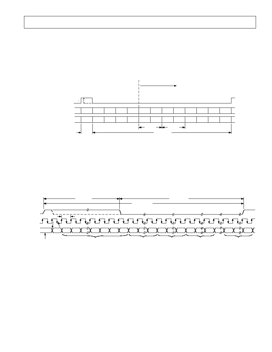
AD1819A
≠19≠
REV. 0
The AC-Link protocol provides for a special 16-bit time slot (Slot 0) wherein each bit conveys a valid tag for its corresponding time
slot within the current audio frame. A "1" in a given bit position of Slot 0 indicates that the corresponding time slot within the cur-
rent audio frame has been assigned to a data stream, and contains valid data. If a slot is "tagged" invalid, it is the responsibility of the
source of the data, (AD1819A for the input stream, AC '97 controller for the output stream), to stuff all bit positions with 0s during
that slot's active time. The AD1819A stuffs all invalid slots with zeros and ignores invalid input slots.
Additionally, for power savings, all clock, sync, and data signals can be halted.
For multiple codec operations, the AD1819A supports an enhanced mode for communicating with up to two additional codecs. The
Slave 1 AD1819A codec uses Slots 5 and 6, while Slave 2 uses Slots 7 and 8 as shown in the following diagram.
SLAVE 1
1
2
3
4
5
6
7
8
9
10
11
12
SLOT # ....
SYNC
OUTGOING STREAMS
INCOMING STREAMS
TAG
RSRVD
RSRVD
RSRVD
CMD
ADR
CMD
DATA
PCM
LEFT
PCM
RIGHT
PCM
LEFT
PCM
RIGHT
PCM
LEFT
PCM
RIGHT
TAG
RSRVD
RSRVD
RSRVD
PCM
LEFT
PCM
RIGHT
PCM
LEFT
PCM
RIGHT
PCM
LEFT
PCM
RIGHT
STATUS
DATA
STATUS
ADR
RSRVD
RSRVD
ENHANCED MODE
SLAVE 2
DATA PHASE
TAG
PHASE
Figure 9. Standard Bidirectional Audio Frame
AC-Link Audio Output Frame (SDATA_OUT)
The audio output frame data streams correspond to the multiplexed bundles of all digital output data targeting AD1819A's DAC
inputs and control registers. As briefly mentioned earlier, each audio output frame supports up to twelve 20-bit outgoing data time
slots. Slot 0 is a special reserved time slot containing 16 bits that are used for AC-Link protocol infrastructure.
Within Slot 0 the first bit is a global bit (SDATA_OUT Slot 0, Bit 15), which flags the validity for the entire audio frame. If the
"Valid Frame" bit is a 1, this indicates that the current audio frame contains at least one slot time of valid data. The next 12-bit
positions sampled by AC '97 indicate which of the corresponding 12 time slots contain valid data. In this way input DAC data
streams of differing sample rates can be transmitted across the AC-Link at its fixed 48 kHz audio frame rate. The following diagram
illustrates the time-slot-based AC-Link protocol.
END OF PREVIOUS
AUDIO FRAME
TIME SLOT "VALID"
BITS
(1) = TIME SLOT CONTAINS VALID PCM DATA
TAG PHASE
20.8 s (48kHz)
DATA PHASE
SLOT 1
SLOT 2
SLOT 3
SLOT 12
SYNC
BIT_CLK
CODEC
READY
SLOT(1) SLOT(2)
SLOT(12)
"0"
"0"
"0"
19
0
19
0
0
0
19
19
12.2888MHz
81.4ns
SDATA_IN
Figure 10. AC-Link Audio Output Frame
A new audio output frame begins with a low-to-high transition of SYNC. SYNC is synchronous to the rising edge of BIT_CLK. On
the immediately following falling edge of BIT_CLK, the AD1819A samples the assertion of SYNC. This falling edge marks the time
when both sides of AC-Link are aware of the start of a new audio frame. On the next rising edge of BIT_CLK, the AC '97 controller
transitions SDATA_OUT into the first bit position of Slot 0 (Valid Frame Bit). Each new bit position is presented to AC-Link on a
rising edge of BIT_CLK, and subsequently sampled by AD1819A on the following falling edge of BIT_CLK. This sequence ensures
that data transitions, and subsequent sample points for both incoming and outgoing data streams are time aligned.

AD1819A
≠20≠
REV. 0
VALID
FRAME
SLOT (1) SLOT (2)
AC '97 CONTROLLER SAMPLES
FIRST SDATA_OUT BIT OF FRAME HERE
SYNC
BIT_CLK
SDATA_OUT
AD1819A SAMPLES SYNC ASSERTION HERE
END OF PREVIOUS
AUDIO FRAME
Figure 11. Start of an Audio Output Frame
SDATA_OUT's composite stream is MSB justified (MSB first) with all nonvalid slots' bit positions stuffed with 0s by the
AC '97 controller. The AD1819A ignores invalid slots.
In the event that there are less than 20 valid bits within an assigned and valid time slot, the AC '97 controller always stuffs all trailing
nonvalid bit positions of the 20-bit slot with 0s. The AD1819A ignores unused bits.
As an example, consider an 8-bit sample stream being played out to one of the AD1819A's DACs. The first 8-bit positions are pre-
sented to the DAC (MSB justified), followed by the next 12 bit positions, which are stuffed with 0s by the AC '97 controller.
When mono audio sample streams are output from the AC '97 controller, it is necessary that BOTH left and right stream time slots
be filled with the same data.
Slot 1: Command Address Port
The command port is used to control features and request status (see Audio Input Frame Slots l and 2) for AD1819A functions
including, but not limited to, mixer settings and power management (refer to the control register section of this specification).
The control interface architecture supports up to sixty-four 16-bit read/write registers, addressable on even byte boundaries. Only the
even registers (00h, 02h, etc.) are valid, odd register (01h, 03h, etc.) accesses are discouraged (defaulting to the preceding even byte
boundary--i.e., a read to 01h will return the 16-bit contents of 00h). Note that shadowing of the control register file on the AC '97
controller is an option left open to the implementation of the AC '97 controller. The AD1819A's control register file is readable as
well as writable.
Audio output frame Slot 1 communicates control register address, and write/read command information to AD1819A.
Command Address Port Bit Assignments:
Bit (19)
Read/Write Command
(1 = Read, 0 = Write)
Bit (18:12)
Control Register Index
(64 16-Bit Locations, Addressed On Even Byte Boundaries)
Bit (11:0)
Reserved
(Stuffed with 0s)
The first bit (MSB) sampled by the AD1819A indicates whether the current control transaction is a read or a write operation. The
following 7-bit positions communicate the targeted control register address. The trailing 12-bit positions within the slot are reserved.
Slot 2: Command Data Port
The command data port is used to deliver 16-bit control register write data in the event that the current command port operation is a
write cycle (as indicated by Slot 1, Bit 19).
Bit (19:4)
Control Register Write Data
(Stuffed with 0s If Current Operation Is Not a Write)
Bit (3:0)
Reserved
(Stuffed with 0s)
If the current command port operation is not a write, the entire slot time should be stuffed with 0s by the AC '97 controller.
Slot 3: PCM Playback Left Channel
Audio output frame Slot 3 is the composite digital audio left playback stream. In a typical "Games Compatible" PC this slot is com-
posed of standard PCM (.wav) output samples digitally mixed (on the AC '97 controller or host processor) with music synthesis
output samples. If a sample stream of resolution less than 20 bits is transferred, the AC '97 controller should stuff all trailing
nonvalid bit positions within this time slot with 0s.
Slot 4: PCM Playback Right Channel
Audio output frame Slot 4 is the composite digital audio right playback stream. In a typical "Games Compatible" PC this slot is
composed of standard PCM (.wav) output samples digitally mixed (on the AC '97 controller or host processor) with music synthesis
output samples. If a sample stream of resolution less than 20 bits is transferred, the AC '97 controller should stuff all trailing nonvalid bit
positions within this time slot with 0s.
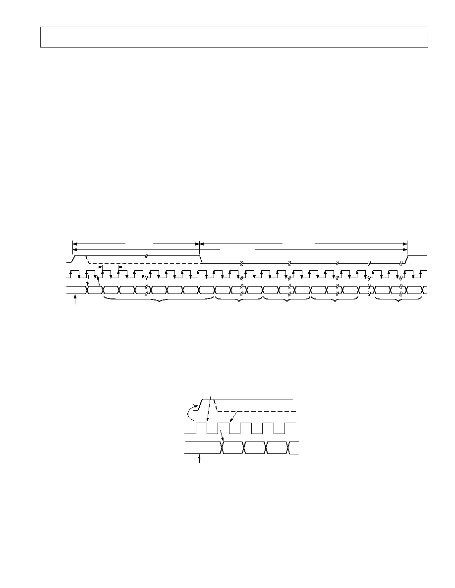
AD1819A
≠21≠
REV. 0
Slot 5≠Slot 8: Multicodec Communication
∑ Slot 5 Slave 1 PCM Playback Left Channel
∑ Slot 6 Slave 1 PCM Playback Right Channel
∑ Slot 7 Slave 2 PCM Playback Left Channel
∑ Slot 8 Slave 2 PCM Playback Right Channel
Slot 6≠Slot 12: Reserved
Audio output frame Slot 6 to Slot 12 are reserved for future use and should always be stuffed with 0s by the digital controller.
AC-Link Audio Input Frame (SDATA_IN)
The audio input frame data streams correspond to the multiplexed bundles of all digital input data targeting the AC '97 controller.
As is the case for audio output frame, each AC-Link audio input frame consists of twelve 20-bit time slots. Slot 0 is a special reserved
time slot containing 16 bits used for AC-Link protocol infrastructure.
Within Slot 0 the first bit is a global bit (SDATA_IN Slot 0, Bit 15) which flags whether or not AD1819A is in the "Codec Ready"
state. If the "Codec Ready" bit is a 0, this indicates that AD1819A is not ready for normal operation. This condition is normal fol-
lowing the deassertion of power-on reset, for example, while AD1819A's voltage references settle. When the AC-Link "Codec Ready"
indicator bit is a 1, it indicates that the AC-Link and AD1819A control and status registers are in a fully operational state and all
subsections are ready.
Prior to any attempts at putting AD1819A into operation the AC '97 controller should poll the first bit in the audio input frame
(SDATA_IN Slot 0, Bit 15) for an indication that the AD1819A has asserted "Codec Ready." Once the AD1819A is sampled, "Codec
Ready" is asserted the next 12-bit positions sampled by the AC '97 controller indicate which of the corresponding 12 time slots are
assigned to input data streams and that they contain valid data. The following diagram illustrates the time-slot-based AC-Link protocol.
END OF PREVIOUS
AUDIO FRAME
TIME SLOT "VALID"
BITS
(1) = TIME SLOT CONTAINS VALID PCM DATA
TAG PHASE
20.8 s (48kHz)
DATA PHASE
SLOT 1
SLOT 2
SLOT 3
SLOT 12
SYNC
BIT_CLK
SLOT(1) SLOT(2)
SLOT(12)
"0"
"0"
"0"
19
0
19
0
0
0
19
19
12.288MHz
81.4ns
SDATA_IN
READY
CODEC
Figure 12. AC-Link Audio Input Frame
A new audio input frame begins with a low-to-high transition of SYNC. SYNC is synchronous to the rising edge of BIT_CLK. On
the immediately following falling edge of BIT_CLK, the AD1819A samples the assertion of SYNC. This falling edge marks the time
when both sides of AC-Link are aware of the start of a new audio frame. On the next rising of BIT_CLK, the AD1819A transitions
SDATA_IN into the first bit position of Slot 0 ("Codec Ready" bit). Each new bit position is presented to AC-Link on a rising edge of
BIT_CLK, and subsequently sampled by the AC '97 controller on the following falling edge of BIT_CLK. This sequence ensures
that data transitions, and subsequent sample points for both incoming and outgoing data streams, are time aligned.
SLOT (1) SLOT (2)
AC '97 CONTROLLER SAMPLES
FIRST SDATA_IN BIT OF FRAME HERE
SYNC
BIT_CLK
SDATA_IN
AD1819A SAMPLES SYNC ASSERTION HERE
END OF PREVIOUS
AUDIO FRAME
CODEC
READY
Figure 13. Start of an Audio Input Frame
SDATA_IN's composite stream is MSB justified (MSB first) with all nonvalid bit positions (for assigned and/or unassigned time
slots) stuffed with 0s by AD1819A.
Slot 0: Tag Phase SDATA_IN
The AD1819A is capable of sampling data from 7 kHz to 48 kHz with a resolution of 1 kHz. To enable a sample rate other than the
default 48 kHz, set the DRQEN bit (Register 74h Bit 11). This allows DAC request bits (these are low active) to be output on the
SDATA_IN stream. The digital controller should monitor the ADC valid bits to determine when the codec has valid data ready to
send.

AD1819A
≠22≠
REV. 0
TAG Phase Bit Assignments:
Bit (15)
Codec Ready
Bit (14)
Slot 1 Valid
Bit (13)
Slot 2 Valid
Bit (12)
Slot 3 Valid/ADC Left Data Is Valid on Slot 3
Bit (11)
Slot 4 Valid/ADC Right Data Is Valid on Slot 4
Bit (10)
Slot 5 Valid/ADC Left Data Slave 1 Valid on Slot 5
Bit (9)
Slot 6 Valid/ADC Right Data Slave 1 Valid on Slot 6
Bit (8)
Slot 7 Valid/ADC Left Data Slave 2 Valid on Slot 7
Bit (7)
Slot 8 Valid/ADC Right Data Slave 2 Valid on Slot 8
Bit (6:0)
Not Used
Slot 1: Status Address Port
The status port is used to monitor status for AD1819A functions including, but not limited to, mixer settings and power manage-
ment.
Audio input frame Slot 1's stream echoes the control register index, for historical reference, for the data to be returned in Slot 2
(assuming that Slots 1 and 2 had been tagged "valid" by the AD1819A during Slot 0).
Status Address Port Bit Assignments:
Bit (19)
RESERVED
(Stuffed with 0)
Bit (18:12)
Control Register Index
(Echo of Register Index for Which Data Is Being Returned)
Bit (11)
DAC Request Slot 3
(0 = Request, 1 = No Request)
Bit (10)
DAC Request Slot 4
(0 = Request, 1 = No Request)
Bit (9)
DAC Request Slot 5
(0 = Request, 1 = No Request); Slave 1
Bit (8)
DAC Request Slot 6
(0 = Request, 1 = No Request); Slave 1
Bit (7)
DAC Request Slot 7
(0 = Request, 1 = No Request); Slave 2
Bit (6)
DAC Request Slot 8
(0 = Request, 1 = No Request); Slave 2
Bit (5:0)
RESERVED
(Stuffed with 0s)
The first bit (MSB) generated by the AD1819A is always stuffed with a 0. The following 7-bit positions communicate the associated
control register address, and the trailing 12-bit positions are stuffed with 0s by the AD1819A.
Slot 2: Status Data Port
The status data port delivers 16-bit control register read data.
Bit (19:4)
Control Register Read Data
(Stuffed with 0s If Tagged "Invalid" by AD1819A)
Bit (3:0)
RESERVED
(Stuffed with 0s)
If Slot 2 is tagged "invalid" by the AD1819A, the entire slot will be stuffed with 0s by the AD1819A.
Slot 3: PCM Record Left Channel
Audio input frame Slot 3 is the left channel output of the AD1819A's input MUX, post-ADC.
AD1819A transmits its ADC output data (MSB first), and stuffs the trailing nonvalid bit positions with 0s to fill out its 20-bit time slot.
Slot 4: PCM Record Right Channel
Audio input frame Slot 4 is the right channel output of the AD1819A's input MUX, post-ADC.
AD1819A transmits its ADC output data (MSB first), and stuffs the trailing nonvalid bit positions with 0s to fill out its 20-bit time slot.
Slot 5≠Slot 8: Multicodec Communication
∑ Slot 5 Slave 1 PCM Record Left Channel
∑ Slot 6 Slave 1 PCM Record Right Channel
∑ Slot 7 Slave 2 PCM Record Left Channel
∑ Slot 8 Slave 2 PCM Record Right Channel
Slot 9≠Slot 12: Reserved
Audio input frame Slots 9≠12 are reserved for future use and are always stuffed with 0s by the AD1819A.
AC-Link Low Power Mode
The AC-Link signals can be placed in a low power mode. When the AD1819A's Power-Down Register (26h) is programmed to the
appropriate value, both BIT_CLK and SDATA_IN will be brought to a logic low voltage level.

AD1819A
≠23≠
REV. 0
SLOT 12
PREVIOUS
FRAME
TAG
SDATA_IN
BIT_CLK
SYNC
SDATA_OUT
SLOT 12
PREVIOUS
FRAME
TAG
WRITE TO
0x26
DATA
PR4
NOTE:
BIT_CLK NOT TO SCALE
Figure 14. AC-Link Power-Down Timing
BIT_CLK and SDATA_IN are transitioned low immediately following the decode of the write to the Power-Down Register (26h)
with PR4. When the AC '97 controller driver is at the point where it is ready to program the AC-Link into its low power mode, Slots
(1 and 2) must be the only valid stream in the audio output frame.
The AC '97 controller should also drive SYNC and SDATA_OUT low after programming AD1819A to this low power "halted" mode.
Once AD1819A has been instructed to halt BIT_CLK, a special "wake-up" protocol must be used to bring the AC-Link to the active
mode, since normal audio output and input frames can not be communicated in the absence of BIT_CLK.
Waking up the AC-Link
There are two methods for bringing the AC-Link out of a low power, halted mode. Regardless of the method, it is the AC '97
controller that performs the wake-up task.
AC-Link protocol provides for a "Cold AC '97 Reset," and a "Warm AC '97 Reset." The current power-down state would
ultimately dictate which form of AC '97 reset is appropriate. Unless a "cold" or "register" reset (a write to the Reset Register) is
performed, wherein the AD1819A registers are initialized to their default values, registers are required to keep state during all power-
down modes. The Serial Configuration Register (0x74) maintains state during a register reset.
Once powered down, reactivation of the AC-Link via reassertion of the SYNC signal may be immediate. When the AD1819A powers
up, it indicates readiness via the Codec Ready Bit (Input Slot 0, Bit 15).
Cold AC '97 Reset
A cold reset is achieved by asserting
RESET for at least the minimum specified time. SYNC and SDATA_IN should be held low during
the rising edge of
RESET. By driving RESET, BIT_CLK and SDATA_IN will be activated, and all AD1819A control registers will be
initialized to their default power-on reset values.
RESET is an asynchronous AD1819A input.
Warm AC '97 Reset
A warm AC '97 reset will reactivate the AC-Link without altering the current AD1819A register values. A warm reset is signaled
by driving SYNC high for a minimum of 1
µ
s in the absence of BIT_CLK.
Within normal audio frames SYNC is a synchronous AD1819A input. In the absence of BIT_CLK, however, SYNC is treated as an
asynchronous input used in the generation of a warm reset to the AD1819A.

AD1819A
≠24≠
REV. 0
MULTIPLE CODE CONFIGURATION
Setting Up Multiple Codecs
The AD1819A may be used with up to two additional AD1819
or AD1819A codecs. In order to configure the codecs as Mas-
ter, Slave 1 or Slave 2, refer to the following table.
CS1
CS0
Configuration
0
0
Slave 1 Codec
0
1
Slave 2 Codec
1
0
Master Codec
1
1
AC '97 Mode Codec
0 = Ground; 1 = V
DD
.
The XTAL_IN pin on the Slave Codecs "must" be tied to
ground and the CHAIN_IN pin "must" be tied to ground on
the last codec Slave 1 (on a 2-codec design) or SLAVE 2 (on a
3-codec design). See Figures 15, 16 and 17.
Configure the Codec Resources
Programing REGM (2:0) bits in the Serial Configuration Regis-
ter (74h) allows the digital controller read write access to all the
internal registers on each codec according to the following table.
REGM2
REGM1
REGM0
Read
Write
0
0
0
x
x
0
0
1
Master
Master
0
1
0
Slave 1
Slave 1
0
1
1
Master
Master, Slave 1
1
0
0
Slave 2
Slave 2
1
0
1
Master
Master, Slave 2
1
1
0
Slave 1
Slave 1, Slave 2
1
1
1
Master
Master, Slave 1, Slave 2
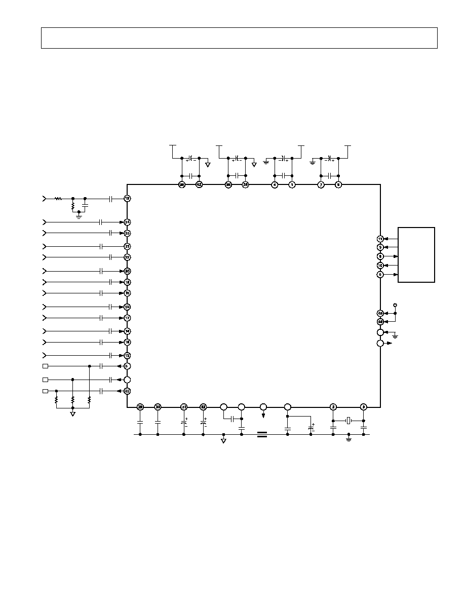
AD1819A
≠25≠
REV. 0
RESET
SDATA_OUT
SDATA_IN
SYNC
BIT_CLK
CS0
CS1
CHAIN_IN
CHAIN_CLK
DIGITAL
CONTROLLER
DV
DD
10 F TANT
100nF
10 F TANT
100nF
100nF
10 F TANT
100nF
10 F TANT
+5AV
DD
+5AV
DD
+5DV
DD
+5DV
DD
AV
DD2
AV
SS2
AV
DD1
AV
SS
DV
SS1
DV
DD1
DV
SS2
DV
DD2
AFILT1 AFILT2
FILT_L
PHONE_IN
MONO_OUT
LINE_OUT_R
LINE_OUT_L
1 F
1 F
1 F
1 F
47k
47k
47k
1 F
24.576MHz
22pF
NP0
22pF
NP0
10 F
TANT
100nF
47nF
2.25V
DC
100nF
1 F
270pF
NP0
270pF
NP0
FILT_R
CX3D
RX3D
V
REFOUT
V
REF
XTAL_IN
XTAL_OUT
600Z
ANALOG GROUND
DIGITAL GROUND
AD1819A
PC_BEEP
LINE_IN_R
LINE_IN_L
MIC1
MIC2
CD_R
CD_L
CD_GND
VIDEO_L
VIDEO_R
AUX_L
AUX_R
1 F
1 F
1 F
1 F
1 F
1 F
1 F
7
36
34
33
27
1.37k
47
48
4.99k
100nF
100nF
1 F
1 F
1 F
1 F
28
Figure 15. Recommended One Codec Application Circuit
APPLICATIONS CIRCUITS
The AD1819A has been designed to require a minimum amount
of external circuitry. The recommended applications circuits are
shown in Figures 15≠18. Reference designs for the AD1819A
are available and may be obtained by contacting your local
Analog Devices' sales representative or authorized distributor.
Example shell programs for establishing a communications path
between the AD1819A and an ADSP-21xx DSP are also available.
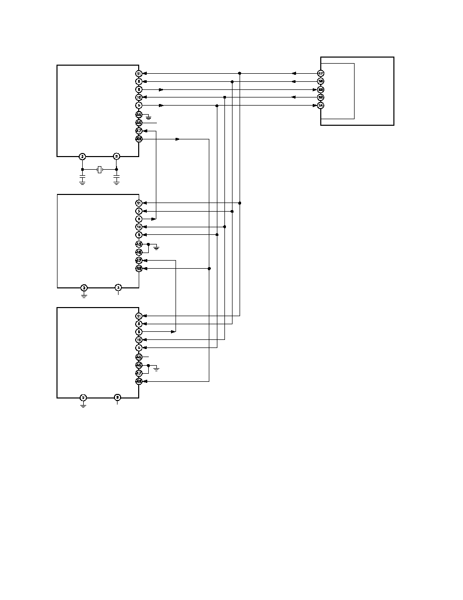
AD1819A
≠26≠
REV. 0
RESET
SDATA_OUT
SDATA_IN
SYNC
BIT_CLK
CS0
CS1
CHAIN_IN
CHAIN_CLK
AD1819A
MASTER
XTAL_IN
XTAL_OUT
22pF
NP0
22pF
NP0
24.576MHz
FL0
DT0
DR0
RFS0
SCLK0
SPORT0
RESET
SDATA_OUT
SDATA_IN
SYNC
BIT_CLK
DV
DD
DIGITAL
CONTROLLER
(ADSP-2181)
DV
DD
RESET
SDATA_OUT
SDATA_IN
SYNC
BIT_CLK
CS0
CS1
CHAIN_IN
CHAIN_CLK
AD1819A
SLAVE 1
XTAL_IN
XTAL_OUT
RESET
SDATA_OUT
SDATA_IN
SYNC
BIT_CLK
CS0
CS1
CHAIN_IN
CHAIN_CLK
AD1819A
SLAVE 2
XTAL_IN
XTAL_OUT
Figure 16. Three Codec System Example
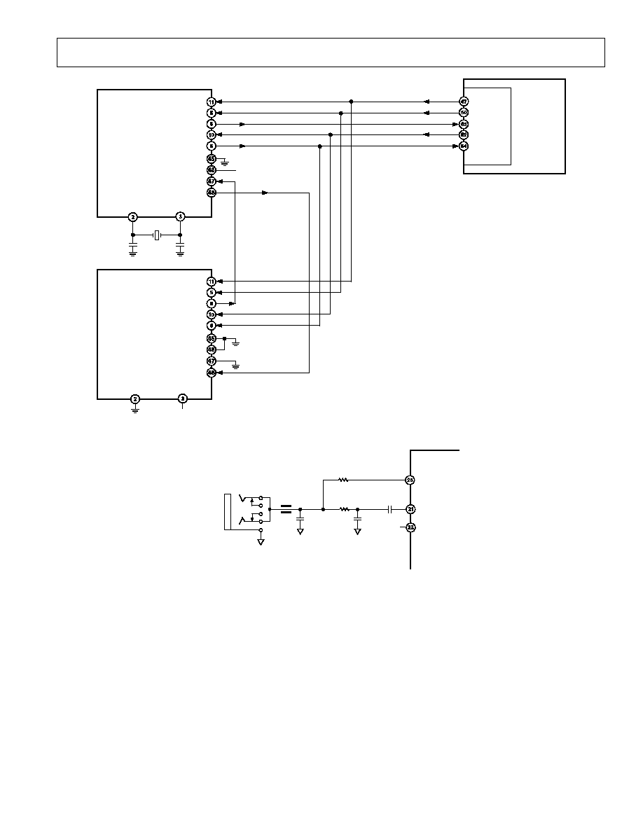
AD1819A
≠27≠
REV. 0
RESET
SDATA_OUT
SDATA_IN
SYNC
BIT_CLK
CS0
CS1
CHAIN_IN
CHAIN_CLK
AD1819A
MASTER
XTAL_IN
XTAL_OUT
22pF
NP0
22pF
NP0
24.576MHz
FL0
DT0
DR0
RFS0
SCLK0
SPORT0
RESET
SDATA_OUT
SDATA_IN
SYNC
BIT_CLK
DIGITAL
CONTROLLER
(ADSP-2181)
DV
DD
RESET
SDATA_OUT
SDATA_IN
SYNC
BIT_CLK
CS0
CS1
CHAIN_IN
CHAIN_CLK
AD1819A
SLAVE 1
XTAL_IN
XTAL_OUT
Figure 17. Two Codec System Example
2.21k *
100
100nF
10nF*
NC
MIC1**
MIC2
AD1819A
V
REFOUT
FB
100pF
200Hz < FREQUENCY RESPONSE < 5kHz @ ≠3dB
NOTES:
*MAY NEED TO OPTIMIZE TO SUIT MICROPHONE
**SELECT MIC1 AND MAX GAIN 20dB +12dB for 10mV
RMS MICROPHONE OUTPUT.
MIC
INPUT
10mV RMS
(mean)
Figure 18. Microphone Input
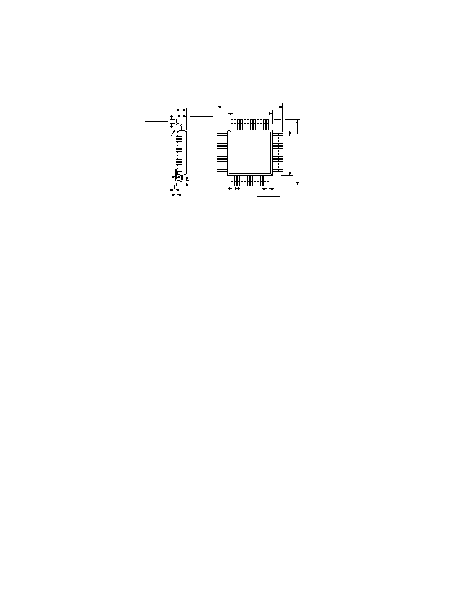
AD1819A
≠28≠
REV. 0
C3261≠8≠3/98
PRINTED IN U.S.A.
OUTLINE DIMENSIONS
Dimensions shown in inches and (mm).
48-Terminal TQFP
(ST-48)
0.354 (9.00) BSC
0.276 (7.0) BSC
1
12
13
25
24
36
37
48
TOP VIEW
(PINS DOWN)
0.276 (7.0) BSC
0.354 (9.00) BSC
0.011 (0.27)
0.006 (0.17)
0.019 (0.5)
BSC
SEATING
PLANE
0.063 (1.60) MAX
0∞ MIN
0∞ ≠ 7∞
0.006 (0.15)
0.002 (0.05)
0.030 (0.75)
0.018 (0.45)
0.057 (1.45)
0.053 (1.35)
0.030 (0.75)
0.018 (0.45)
0.007 (0.18)
0.004 (0.09)