Document Outline
- FEATURES
- APPLICATIONS
- PRODUCT OVERVIEW
- FUNCTIONAL BLOCK DIAGRAM
- SPECIFICATIONS
- TEST CONDITIONS
- TIMING SPECIFICATIONS
- TEMPERATURE RANGE
- ABSOLUTE MAXIMUM RATINGS
- ORDERING GUIDE
- PIN CONFIGURATION
- PIN FUNCTION DESCRIPTIONS
- Typical Performance Characteristics
- TERMINOLOGY
- Dynamic Range
- Signal-to-(Total Harmonic Distortion + Noise) [S/(THD + N)]
- Pass Band
- Pass-Band Ripple
- Stop Band
- Gain Error
- Interchannel Gain Mismatch
- Gain Drift
- Crosstalk (EIAJ Method)
- Power Supply Rejection
- Group Delay
- Group Delay Variation
- ACRONYMS
- FUNCTIONAL OVERVIEW
- ADCs
- DACs
- DAC and ADC Coding
- Clock Signals
- RESET and Power-Down
- Power Supply and Voltage Reference
- Serial Control Port
- Serial Data PortsÑData Format
- Packed Modes
- Auxiliary (TDM) Mode
- CONTROL/STATUS REGISTERS
- DAC CONTROL REGISTERS
- Sample Rate
- Power-Down/Reset
- DAC Data-Word Width
- DAC Data Format
- De-emphasis
- Mute DAC
- Stereo Replicate
- DAC Volume Control
- ADC CONTROL REGISTERS
- ADC Peak Level
- Sample Rate
- ADC Power-Down
- High-Pass Filter
- ADC Data-Word Width
- ADC Data Format
- Master/Slave Auxiliary Mode
- ADC Peak Readback
- OUTLINE DIMENSIONS
- Revision History

REV. B
Information furnished by Analog Devices is believed to be accurate and
reliable. However, no responsibility is assumed by Analog Devices for its
use, nor for any infringements of patents or other rights of third parties that
may result from its use. No license is granted by implication or otherwise
under any patent or patent rights of Analog Devices. Trademarks and
registered trademarks are the property of their respective companies.
One Technology Way, P.O. Box 9106, Norwood, MA 02062-9106, U.S.A.
Tel: 781/329-4700
www.analog.com
Fax: 781/326-8703
© 2003 Analog Devices, Inc. All rights reserved.
AD1839
2 ADC, 6 DAC,
96 kHz, 24-Bit -
Codec
FEATURES
5 V Stereo Audio System with 3.3 V Tolerant
Digital Interface
Supports up to 96 kHz Sample Rates
192 kHz Sample Rate Available on One DAC
Supports 16-/20-/24-Bit Word Lengths
Multibit - Modulators with
Perfect Differential Linearity Restoration for
Reduced Idle Tones and Noise Floor
Data Directed Scrambling DACs--Least
Sensitive to Jitter
Single-Ended Output
ADCs: ≠95 dB THD + N, 105 dB SNR and
Dynamic Range
DACs: ≠92 dB THD + N, 108 dB SNR and
Dynamic Range
On-Chip Volume Controls per Channel with
1024 Step Linear Scale
DAC and ADC Software Controllable Clickless Mutes
Digital De-emphasis Processing
Supports 256 f
S
, 512 f
S,
and 768 f
S
Master
Mode Clocks
Power-Down Mode Plus Soft Power-Down Mode
Flexible Serial Data Port with Right-Justified, Left-
Justified, I
2
S Compatible, and DSP Serial Port Modes
TDM Interface Mode Supports 8 In/8 Out Using a
Single SHARC
Æ
SPORT
52-Lead MQFP Plastic Package
APPLICATIONS
DVD Video and Audio Players
Home Theater Systems
Automotive Audio Systems
Audio/Visual Receivers
Digital Audio Effects Processors
PRODUCT OVERVIEW
The AD1839 is a high performance single-chip codec featuring
three stereo DACs and one stereo ADC. Each DAC comprises
a high performance digital interpolation filter, a multibit -
modulator featuring Analog Devices' patented technology, and
a continuous-time voltage out analog section. Each DAC has
independent volume control and clickless mute functions. The
ADC comprises two 24-bit conversion channels with multibit
- modulators and decimation filters.
The AD1839 also contains an on-chip reference with a nominal
value of 2.25 V.
The AD1839 contains a flexible serial interface that allows
for glueless connection to a variety of DSP chips, AES/EBU
receivers, and sample rate converters. The AD1839 can be
configured in left-justified, right-justified, I
2
S, or DSP com-
patible serial modes. Control of the AD1839 is achieved by
means of an SPI
Æ
compatible serial port. While the AD1839
can be operated from a single 5 V supply, it also features a
separate supply pin for its digital interface that allows the device
to be interfaced to other devices using 3.3 V power supplies.
The AD1839 is available in a 52-lead MQFP package and is
specified for the industrial temperature range of ≠40∫C to +85∫C.
FUNCTIONAL BLOCK DIAGRAM
OUTL1
CONTROL PORT
CLOCK
FILTD
FILTR
ADCLP
ADCLN
ADCRP
ADCRN
DLRCLK
DBCLK
DSDATA1
DSDATA2
DSDATA3
DAUXDATA
MCLK
ASDATA
ABCLK
ALRCLK
ODVDD
DVDD
AVDD
AVDD
DVDD
AGND
DGND
CIN
CLATCH
CCLK
COUT
DIGITAL
FILTER
PD/RST M/S
-
ADC
VOLUME
SERIAL DATA
I/O PORT
DIGITAL
FILTER
-
DAC
V
REF
OUTR1
VOLUME
OUTL2
VOLUME
DIGITAL
FILTER
-
DAC
OUTR2
VOLUME
OUTL3
VOLUME
DIGITAL
FILTER
-
DAC
OUTR3
VOLUME
DIGITAL
FILTER
-
ADC
AAUXDATA3
AD1839
AGND AGND AGND
DGND

REV. B
≠2≠
AD1839≠SPECIFICATIONS
TEST CONDITIONS
Supply Voltages (AV
DD
, DV
DD
) 5.0 V
Ambient Temperature
25
C
Input Clock
12.288 MHz, (256 f
S
Mode)
DAC Input Signal
1.0078125 kHz, 1.0 dBFS
ADC Input Signal
1.0078125 kHz, 0 dBFS
Input Sample Rate (f
S
)
48 kHz
Measurement Bandwidth
20 Hz to 20 kHz
Word Width
24 Bits
Load Capacitance
100 pF
Load Impedance
47 k
W
Performance of all channels is identical (exclusive of the Interchannel Gain Mismatch and Interchannel Phase Deviation specifications).
Parameter
Min
Typ
Max
Unit
ANALOG-TO-DIGITAL CONVERTERS
ADC Resolution
24
Bits
Dynamic Range (20 Hz to 20 kHz, ≠60 dB Input)
No Filter
103
dB
A-Weighted
100
105
dB
Total Harmonic Distortion + Noise (THD+N)
≠95
≠88.5
dB
Interchannel Isolation
100
dB
Interchannel Gain Mismatch
0.025
dB
Analog Inputs
Differential Input Range (
± Full Scale)
≠2.828
+2.828
V
Common-Mode Input Voltage
2.25
V
Input Impedance
4
k
W
Input Capacitance
15
pF
V
REF
2.25
V
DC Accuracy
Gain Error
±5
%
Gain Drift
35
ppm/∫C
DIGITAL-TO-ANALOG CONVERTERS
DAC Resolution
Dynamic Range (20 Hz to 20 kHz, ≠60 dBFS Input)
No Filter
103
105
dB
With A-Weighted Filter
105
108
dB
Total Harmonic Distortion + Noise
≠92
≠90
dB
Interchannel Isolation
110
dB
DC Accuracy
Gain Error
±4
%
Interchannel Gain Mismatch
0.025
dB
Gain Drift
200
ppm/
C
Interchannel Phase Deviation
±0.1
Degrees
Volume Control Step Size (1023 Linear Steps)
0.098
%
Volume Control Range (Max Attenuation)
60
dB
Mute Attenuation
≠100
dB
De-emphasis Gain Error
±0.1
dB
Full-Scale Output Voltage at Each Pin
1.0 (2.8)
V rms (V p-p)
Output Resistance at Each Pin
180
W
Common-Mode Output Voltage
2.25
V
ADC DECIMATION FILTER, 48 kHz
*
Pass Band
21.77
kHz
Pass-Band Ripple
±0.01
dB
Stop Band
26.23
kHz
Stop-Band Attenuation
120
dB
Group Delay
910
ms

REV. B
AD1839
≠3≠
Parameter
Min
Typ
Max
Unit
ADC DECIMATION FILTER, 96 kHz
*
Pass Band
43.54
kHz
Pass-Band Ripple
±0.01
dB
Stop Band
52.46
kHz
Stop-Band Attenuation
120
dB
Group Delay
460
ms
DAC INTERPOLATION FILTER, 48 kHz
*
Pass Band
21.77
kHz
Pass-Band Ripple
±0.06
dB
Stop Band
28
kHz
Stop-Band Attenuation
55
dB
Group Delay
340
ms
DAC INTERPOLATION FILTER, 96 kHz
*
Pass Band
43.54
kHz
Pass-Band Ripple
±0.06
dB
Stop Band
52
kHz
Stop-Band Attenuation
55
dB
Group Delay
160
ms
DAC INTERPOLATION FILTER, 192 kHz
*
Pass Band
81.2
kHz
Pass-Band Ripple
±0.06
dB
Stop Band
97
kHz
Stop-Band Attenuation
80
dB
Group Delay
110
ms
DIGITAL I/O
Input Voltage High
2.4
V
Input Voltage Low
0.8
V
Output Voltage High
ODV
DD
≠ 0.4
V
Output Voltage Low
0.4
V
Leakage Current
±10
mA
POWER SUPPLIES
Supply Voltage (AV
DD
and DV
DD
)
4.5
5.0
5.5
V
Supply Voltage (ODV
DD
)
3.0
DV
DD
V
Supply Current I
ANALOG
84
95
mA
Supply Current I
ANALOG
,
Power-Down
55
67
mA
Supply Current I
DIGITAL
64
74
mA
Supply Current I
DIGITAL
,
Power-Down
1
4.5
mA
Dissipation
Operation, Both Supplies
740
mW
Operation, Analog Supply
420
mW
Operation, Digital Supply
320
mW
Power-Down, Both Supplies
280
mW
Power Supply Rejection Ratio
1 kHz, 300 mV p-p Signal at Analog Supply Pins
≠70
dB
20 kHz, 300 mV p-p Signal at Analog Supply Pins
≠75
dB
*Guaranteed by design.
Specifications subject to change without notice.

REV. B
≠4≠
AD1839
TIMING SPECIFICATIONS
Parameter
Min
Max
Unit
Comments
MASTER CLOCK AND RESET
t
MH
MCLK High
15
ns
t
ML
MCLK Low
15
ns
t
PDR
PD/RST Low
20
ns
SPI PORT
t
CCH
CCLK High
40
ns
t
CCL
CCLK Low
40
ns
t
CCP
CCLK Period
80
ns
t
CDS
CDATA Setup
10
ns
To CCLK Rising
t
CDH
CDATA Hold
10
ns
From CCLK Rising
t
CLS
CLATCH Setup
10
ns
To CCLK Rising
t
CLH
CLATCH Hold
10
ns
From CCLK Rising
t
COE
COUT Enable
15
ns
From CLATCH Falling
t
COD
COUT Delay
20
ns
From CCLK Falling
t
COTS
COUT Three-State
25
ns
From CLATCH Rising
DAC SERIAL PORT
Normal Mode (Slave)
t
DBH
DBCLK High
60
ns
t
DBL
DBCLK Low
60
ns
f
DB
DBCLK Frequency
64 f
S
t
DLS
DLRCLK Setup
10
ns
To DBCLK Rising
t
DLH
DLRCLK Hold
10
ns
From DBCLK Rising
t
DDS
DSDATA Setup
10
ns
To DBCLK Rising
t
DDH
DSDATA Hold
10
ns
From DBCLK Rising
Packed 256 Modes (Slave)
t
DBH
DBCLK High
15
ns
t
DBL
DBCLK Low
15
ns
f
DB
DBCLK Frequency
256 f
S
t
DLS
DLRCLK Setup
10
ns
To DBCLK Rising
t
DLH
DLRCLK Hold
5
ns
From DBCLK Rising
t
DDS
DSDATA Setup
10
ns
To DBCLK Rising
t
DDH
DSDATA Hold
10
ns
From DBCLK Rising
ADC SERIAL PORT
Normal Mode (Master)
t
ABD
ABCLK Delay
25
ns
From MCLK Rising Edge
t
ALD
ALRCLK Delay Low
5
ns
From ABCLK Falling Edge
t
ABDD
ASDATA Delay
10
ns
From ABCLK Falling Edge
Normal Mode (Slave)
t
ABH
ABCLK High
60
ns
t
ABL
ABCLK Low
60
ns
f
AB
ABCLK Frequency
64 f
S
t
ALS
ALRCLK Setup
5
ns
To ABCLK Rising
t
ALH
ALRCLK Hold
15
ns
From ABCLK Rising
Packed 256 Mode (Master)
t
PABD
ABCLK Delay
20
ns
From MCLK Rising Edge
t
PALD
LRCLK Delay
5
ns
From ABCLK Falling Edge
t
PABDD
ASDATA Delay
10
ns
From ABCLK Falling Edge

REV. B
AD1839
≠5≠
Parameter
Min
Max
Unit
Comments
TDM256 MODE (Master)
t
TBD
BCLK Delay
20
ns
From MCLK Rising
t
FSD
FSTDM Delay
5
ns
From BCLK Rising
t
TABD
ASDATA Delay
10
ns
From BCLK Rising
t
TDDS
DSDATA1 Setup
15
ns
To BCLK Falling
t
TDDH
DSDATA1 Hold
15
ns
From BCLK Falling
TDM256 MODE (Slave)
f
AB
BCLK Frequency
256 f
S
t
TBCH
BCLK High
15
ns
t
TBCL
BCLK Low
15
ns
t
TFS
FSTDM Setup
10
ns
To BCLK Falling
t
TFH
FSTDM Hold
10
ns
From BCLK Falling
t
TBDD
ASDATA Delay
10
ns
From BCLK Rising
t
TDDS
DSDATA1 Setup
15
ns
To BCLK Falling
t
TDDH
DSDATA1 Hold
15
ns
From BCLK Falling
AUXILIARY INTERFACE
t
AXDS
AAUXDATA Setup
10
ns
To AUXBCLK Rising
t
AXDH
AAUXDATA Hold
10
ns
From AUXBCLK Rising
t
DXD
DAUXDATA Delay
15
ns
From AUXBCLK Falling
f
ABP
AUXBCLK Frequency
64 f
S
Slave Mode
t
AXBH
AUXBCLK High
15
ns
t
AXBL
AUXBCLK Low
15
ns
t
AXLS
AUXLRCLK Setup
10
ns
To AUXBCLK Rising
t
AXLH
AUXLRCLK Hold
10
ns
From AUXBCLK Rising
Master Mode
t
AUXLRCLK
AUXLRCLK Delay
5
ns
From AUXBCLK Falling
t
AUXBCLK
AUXBCLK Delay
15
ns
From MCLK Rising
Specifications subject to change without notice.
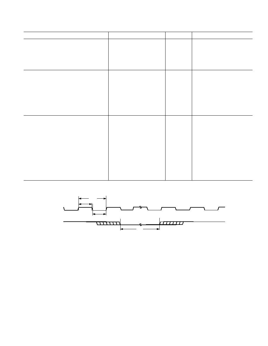
MCLK
t
MH
PD/RST
t
ML
t
PDR
t
MCLK
Figure 1. MCLK and
PD/RST Timing

REV. B
≠6≠
AD1839
CAUTION
ESD (electrostatic discharge) sensitive device. Electrostatic charges as high as 4000 V readily
accumulate on the human body and test equipment and can discharge without detection. Although the
AD1839 features proprietary ESD protection circuitry, permanent damage may occur on devices
subjected to high energy electrostatic discharges. Therefore, proper ESD precautions are recommended
to avoid performance degradation or loss of functionality.
TEMPERATURE RANGE
Parameter
Min
Typ
Max
Unit
Specifications Guaranteed
25
C
Functionality Guaranteed
≠40
+85
C
Storage
≠65
+150
C
ABSOLUTE MAXIMUM RATINGS
*
(T
A
= 25
C, unless otherwise noted.)
AV
DD
, DV
DD
, ODV
DD
to AGND, DGND . . ≠0.3 V to +6.0 V
AGND to DGND . . . . . . . . . . . . . . . . . . . . . ≠0.3 V to +0.3 V
Digital I/O Voltage to DGND . . . . . ≠0.3 V to ODV
DD
+ 0.3 V
Analog I/O Voltage to AGND . . . . . . ≠0.3 V to AV
DD
+ 0.3 V
Operating Temperature Range
Industrial (A Version) . . . . . . . . . . . . . . . . ≠40
C to +85C
*Stresses above those listed under Absolute Maximum Ratings may cause perma-
nent damage to the device. This is a stress rating only; functional operation of the
device at these or any other conditions above those listed in the operational
sections of this specification is not implied. Exposure to absolute maximum rating
conditions for extended periods may affect device reliability.
ORDERING GUIDE
Temperature
Package
Package
Model
Range
Description
Option
AD1839AS
≠40
o
C to +85
o
C
52-Lead MQFP
S-52
AD1839AS-REEL
≠40
o
C to +85
o
C
52-Lead MQFP
S-52
EVAL-AD1839EB
Evaluation Board

REV. B
AD1839
≠7≠
PIN CONFIGURATION
1
2
3
4
5
6
7
8
9
10
11
12
13
AGND
AVDD
OUTR2
NC
OUTL2
NC
OUTR1
NC
OUTL1
NC
PD/RST
CIN
CLATCH
DVDD
NC
OUTL3
DGND
52
51
50
49
48
47
46
45
44
43
42
41
40
FILTD
FILTR
AGND
DAUXDATA
AGND
AVDD
ADCLN
ADCLP
ADCRN
ADCRP
AGND
DGND
CCLK
COUT
ASDATA
ODVDD
MCLK
ALRCLK
ABCLK
AAUXDATA3
DSDATA3
DSDATA2
DSDATA1
AD1839
TOP VIEW
(Not to Scale
)
NC
OUTR3
NC
NC
NC
AGND
AGND
DLRCLK
DBCLK
27
28
29
30
31
32
33
34
35
36
37
38
39
M/S
DVDD
AVDD
14
15
16
17
18
19
20
21
22
23
24
25
26
PIN FUNCTION DESCRIPTIONS
Input/
Pin No.
Mnemonic
Output
Description
1, 39
DVDD
Digital Power Supply. Connect to digital 5 V supply.
2
CLATCH
I
Latch Input for Control Data.
3
CIN
I
Serial Control Input.
4
PD/RST
I
Power-Down/Reset.
5, 10, 16, 24, 30, 34
AGND
Analog Ground.
6, 8, 12, 14, 25,
NC
Not Connected.
27, 31≠33
NC
Not Connected.
7, 13, 26
OUTLx
O
DACx Left Channel Output.
9, 15, 28
OUTRx
O
DACx Right Channel Output.
11, 19, 29
AVDD
Analog Power Supply. Connect to analog 5 V supply.
17
FILTD
Filter Capacitor Connection. Recommended 10
mF/100 nF.
18
FILTR
Reference Filter Capacitor Connection. Recommended 10
mF/100 nF.
20
ADCLN
I
ADC Left Channel Negative Input.
21
ADCLP
I
ADC Left Channel Positive Input.
22
ADCRN
I
ADC Right Channel Negative Input.
23
ADCRP
I
ADC Right Channel Positive Input.
35
M/S
I
ADC
Master/Slave Select.
36
DAUXDATA
I
Auxiliary DAC Input Data.
37
DLRCLK
I/O
DAC LR Clock.
38
DBCLK
I/O
DAC Bit Clock.
40, 52
DGND
Digital Ground.
41≠43
DSDATAx
I
DACx Input Data (Left and Right Channels).
44
AAUXDATA3
I
Auxiliary ADC3 Digital Input.
45
ABCLK
I/O
ADC Bit Clock.
46
ALRCLK
I/O
ADC LR Clock.
47
MCLK
I
Master Clock Input.
48
ODVDD
Digital Output Driver Power Supply.
49
ASDATA
O
ADC Serial Data Output.
50
COUT
O
Output for Control Data.
51
CCLK
I
Control Clock Input for Control Data.

REV. B
≠8≠
AD1839≠Typical Performance Characteristics
FREQUENCY (Normalized to
f
S
)
0
5
MAGNITUDE (dB)
10
≠150
15
≠100
≠50
0
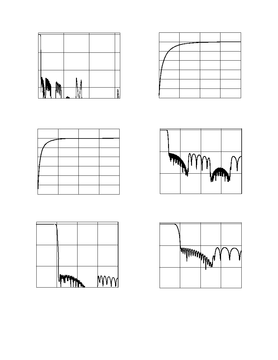
TPC 1. ADC Composite Filter Response
FREQUENCY (Hz)
≠30
0
20
5
MAGNITUDE (dB)
10
15
≠25
≠20
≠15
≠10
≠5
0
5
TPC 2. ADC High-Pass Filter Response, f
S
= 48 kHz
FREQUENCY (Normalized to
f
S
)
≠150
0
2.0
0.5
MAGNITUDE (dB)
1.0
1.5
0
≠100
≠50
TPC 3. ADC Composite Filter Response
(Pass-Band Section)
FREQUENCY (Hz)
≠30
0
20
5
MAGNITUDE (dB)
10
15
≠25
≠20
≠15
≠10
≠5
0
5
TPC 4. ADC High-Pass Filter Response, f
S
= 96 kHz
FREQUENCY (kHz)
0
≠50
≠150
MA
GNITUDE (dB)
≠100
0
200
50
100
150
TPC 5. DAC Composite Filter Response, f
S
= 48 kHz
0
≠50
≠150
≠100
0
200
50
100
150
FREQUENCY (kHz)
MA
GNITUDE (dB)
TPC 6. DAC Composite Filter Response, f
S
= 96 kHz

REV. B
AD1839
≠9≠
0
≠50
0
200
50
100
150
≠100
≠150
FREQUENCY (kHz)
MA
GNITUDE (dB)
TPC 7. DAC Composite Filter Response, f
S
= 192 kHz
0.10
0.05
≠0.10
0
20
5
10
15
0
≠0.05
FREQUENCY (kHz)
MA
GNITUDE (dB)
TPC 8. DAC Composite Filter Response, f
S
= 48 kHz
(Pass-Band Section)
0.2
0.1
≠0.2
0
50
10
20
30
40
0
≠0.1
FREQUENCY (kHz)
MA
GNITUDE (dB)
TPC 9. DAC Composite Filter Response, f
S
= 96 kHz
(Pass-Band Section)
0.10
0.05
≠0.10
0
100
20
40
60
80
0
≠0.05
FREQUENCY (kHz)
MA
GNITUDE (dB)
TPC 10. DAC Composite Filter Response, f
S
= 192 kHz
(Pass-Band Section)

REV. B
≠10≠
AD1839
TERMINOLOGY
Dynamic Range
The ratio of a full-scale input signal to the integrated input noise
in the pass band (20 Hz to 20 kHz), expressed in decibels (dB).
Dynamic range is measured with a ≠60 dB input signal and is
equal to (S/[THD + N]) + 60 dB. Note that spurious harmon-
ics are below the noise with a ≠60 dB input, so the noise level
establishes the dynamic range. The dynamic range is specified
with and without an A-Weight filter applied.
Signal-to-(Total Harmonic Distortion + Noise)
[S/(THD + N)]
The ratio of the root-mean-square (rms) value of the fundamental
input signal to the rms sum of all other spectral components in
the pass band, expressed in decibels (dB).
Pass Band
The region of the frequency spectrum unaffected by the attenu-
ation of the digital decimator's filter.
Pass-Band Ripple
The peak-to-peak variation in amplitude response from equal-
amplitude input signal frequencies within the pass band, expressed
in decibels.
Stop Band
The region of the frequency spectrum attenuated by the digital
decimator's filter to the degree specified by stop-band attenuation.
Gain Error
With identical near full-scale inputs, the ratio of actual output to
expected output, expressed as a percentage.
Interchannel Gain Mismatch
With identical near full-scale inputs, the ratio of outputs of the
two stereo channels, expressed in decibels.
Gain Drift
Change in response to a near full-scale input with a change in
temperature, expressed as parts-per-million (ppm) per
C.
Crosstalk (EIAJ Method)
Ratio of response on one channel with a grounded input to a
full-scale 1 kHz sine wave input on the other channel, expressed
in decibels.
Power Supply Rejection
With no analog input, signal present at the output when a
300 mV p-p signal is applied to power supply pins, expressed in
decibels of full scale.
Group Delay
Intuitively, the time interval required for an input pulse to
appear at the converter's output, expressed in milliseconds (ms).
More precisely, the derivative of radian phase with respect to
radian frequency at a given frequency.
Group Delay Variation
The difference in group delays at different input frequencies.
Specified as the difference between the largest and the smallest
group delays in the pass band, expressed in microseconds (
ms)
ACRONYMS
ADC--Analog-to-Digital Converter
DAC--Digital-to-Analog Converter
DSP--Digital Signal Processor
IMCLK--Internal Master Clock Signal used to clock the ADC
and DAC engines
MCLK--External Master Clock Signal applied to the AD1838

REV. B
AD1839
≠11≠
FUNCTIONAL OVERVIEW
ADCs
There are two ADC channels in the AD1839, configured as a
stereo pair. Each ADC has fully differential inputs. The ADC
section can operate at a sample rate of up to 96 kHz. The ADCs
include on-board digital decimation filters with 120 dB stop-band
attenuation and linear phase response, operating at an over-
sampling ratio of 128 (for 48 kHz operation) or 64 (for 96 kHz
operation).
ADC peak level information for each ADC may be read from
the ADC Peak 0 and ADC Peak 1 registers. The data is supplied
as a 6-bit word with a maximum range of 0 dB to ≠63 dB and a
resolution of 1 dB. The registers will hold peak information until
read; after reading, the registers are reset so that new peak
information can be acquired. Refer to the register description
for details of the format. The two ADC channels have a common
serial bit clock and a left-right framing clock. The clock signals
are all synchronous with the sample rate.
The ADC digital pins, ABCLK and ALRCLK, can be set to
operate as inputs or outputs by connecting the
M/S pin to
ODVDD or DGND, respectively. When the pins are set as
outputs, the AD1839 will generate the timing signals. When
the pins are set as inputs, the timing must be generated by the
external audio controller.
DACs
The AD1839 has six DAC channels arranged as three independent
stereo pairs, with six single-ended analog outputs. Each channel
has its own independently programmable attenuator, adjustable
in 1024 linear steps. Digital inputs are supplied through three
serial data input pins (one for each stereo pair) and a common
frame (DLRCLK) and bit (DBCLK) clock. Alternatively, one
of the packed data modes may be used to access all six channels
on a single TDM data pin. A stereo replicate feature is included
where the DAC data sent to the first DAC pair is also sent to the
other DACs in the part. The AD1839 can accept DAC data at a
sample rate of 192 kHz on DAC 1 only. The stereo replicate
feature can then be used to copy the audio data to the other DACs.
Each of the output pins sits at a dc level of V
REF
and swings
± 1.4 V for a 0 dB digital input signal. A single op amp third
order external low-pass filter is recommended to remove high
frequency noise present on the output pins. Note that the use of
op amps with low slew rate or low bandwidth may cause high
frequency noise and tones to fold down into the audio band;
care should be exercised in selecting these components.
The FILTD pin should be connected to an external grounded
capacitor. This pin is used to reduce the noise of the internal
DAC bias circuitry, thereby reducing the DAC output noise. In
some cases, this capacitor may be eliminated with little effect
on performance.
DAC and ADC Coding
The DAC and ADC output data stream is in a twos complement
encoded format. The word width can be selected from 16-bit,
20-bit, or 24-bit. The coding scheme is detailed in Table I.
Table I. Coding Scheme
Code
Level
01111......1111
+FS
00000......0000
0 (Ref Level)
10000......0000
≠FS
Clock Signals
The DAC and ADC engines in the AD1839 are designed to oper-
ate from a 24.576 MHz internal master clock (IMCLK). This
clock is used to generate 48 kHz and 96 kHz sampling on the
ADC and 48 kHz, 96 kHz, and 192 kHz on the DAC, although
the 192 kHz option is available only on one DAC pair. The
stereo replicate feature can be used to copy this DAC data to
the other DACs if required.
To facilitate the use of the different MCLK values, the AD1839
provides a clock scaling feature. The MCLK scaler can be pro-
grammed via the SPI port to scale the MCLK by a factor of 1
(pass through), 2 (doubling), or 2/3. The default setting of the
MCLK scaler is 2, which will generate 48 kHz sampling from a
12.288 MHz MCLK. Additional sample rates can be achieved
by changing the MCLK value. For example, the CD standard
sampling frequency of 44.1 kHz can be achieved using an
11.2896 kHz MCLK. Figure 2 shows the internal configura-
tion of the clock scaler and converter engines.
DAC ENGINE
CLOCK SCALING
1
2/3
MCLK
12.288MHz
DAC INPUT
INTERPOLATION
FILTER
-
MODULATOR
DAC
48kHz/96kHz/192kHz
ADC OUTPUT
48kHz/96kHz
ANALOG
OUTPUT
ANALOG
INPUT
IMCLK = 24.576MHz
ADC ENGINE
OPTIONAL
HPF
DECIMATOR/
FILTER
-
MODULATOR
2
Figure 2. Modulator Clocking Scheme

REV. B
≠12≠
AD1839
To maintain the highest performance possible, it is recommended
that the clock jitter of the master clock signal be limited to less
than 300 ps rms, measured using the edge-to-edge technique.
Even at these levels, extra noise or tones may appear in the
DAC outputs if the jitter spectrum contains large spectral peaks.
It is highly recommended that the master clock be generated by
an independent crystal oscillator. In addition, it is especially
important that the clock signal should not be passed through an
FPGA or other large digital chip before being applied to the
AD1839. In most cases, this will induce clock jitter due to the
fact that the clock signal is sharing common power and ground
connections with other unrelated digital output signals.
RESET and Power-Down
PD/RST will power down the chip and set the control registers
to their default settings. After
PD/RST is deasserted, an initial-
ization routine will run inside the AD1839 to clear all memories
to zero. This initialization lasts for approximately 20 LRCLK
intervals. During this time, it is recommended that no SPI
writes occur.
Power Supply and Voltage Reference
The AD1839 is designed for 5 V supplies. Separate power supply
pins are provided for the analog and digital sections. These pins
should be bypassed with 100 nF ceramic chip capacitors, as
close to the pins as possible, to minimize noise pickup. A bulk
aluminum electrolytic capacitor of at least 22
mF should also
be provided on the same PC board as the codec. For critical
applications, improved performance will be obtained with
separate supplies for the analog and digital sections. If this is
not possible, it is recommended that the analog and digital
supplies be isolated by means of two ferrite beads in series with
the bypass capacitor of each supply. It is important that the
analog supply be as clean as possible.
The internal voltage reference is brought out on the FILTR pin
and should be bypassed as close as possible to the chip, with a
parallel combination of 10
mF and 100 nF. The reference voltage
may be used to bias external op amps to the common-mode
voltage of the analog input and output signal pins. The current
drawn from the FILTR pin should be limited to less than 50
mA.
Serial Control Port
The AD1839 has an SPI compatible control port to permit
programming the internal control registers for the ADCs and
DACs, and to read the ADC signal levels from the internal
peak detectors. The SPI control port is a 4-wire serial control
port. The format is similar to the Motorola SPI format except
the input data-word is 16 bits wide. The maximum serial bit
clock frequency is 12.5 MHz and may be completely asynchro-
nous to the sample rate of the ADCs and DACs. Figure 3
shows the format of the SPI signal.
Serial Data Ports--Data Format
The ADC serial data output mode defaults to the popular I
2
S
format, where the data is delayed by 1 BCLK interval from the
edge of the LRCLK. By changing Bits 6 to 8 in ADC Control
Register 2, the serial mode can be changed to right-justified
(RJ), left-justified DSP (DSP), or left-justified (LJ). In the RJ
mode, it is necessary to set Bits 4 and 5 to define the width of
the data-word.
The DAC serial data input mode defaults to I
2
S. By changing
Bits 5, 6, and 7 in DAC Control Register 1, the mode can be
changed to RJ, DSP, LJ, or Packed Mode 256. The word width
defaults to 24 bits but can be changed by reprogramming Bits 3
and 4 in DAC Control Register 1.
Packed Modes
The AD1839 has a packed mode that allows a DSP or other
controller to write to all DACs and read all ADCs using one
input data pin and one output data pin. Packed Mode 256
refers to the number of BCLKs in each frame. The LRCLK is
low while data from a left channel DAC or ADC is on the data
pin, and high while data from a right channel DAC or ADC is
on the data pin. DAC data is applied on the DSDATA1 pin,
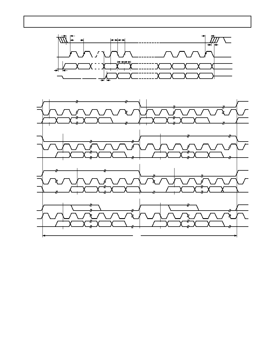
and ADC data is available on the ASDATA pin. Figures 7 to 10
show the timing for the packed mode. Packed mode is available
only for 48 kHz (based on MCLK = 12.288 MHz), and when
the
M/S is low.
Auxiliary (TDM) Mode
A special auxiliary mode is provided to allow three external
stereo ADCs and one external stereo DAC to be interfaced to
the AD1839 to provide 8-in/8-out operation. In addition, this
mode supports glueless interface to a single SHARC DSP serial
port, allowing a SHARC DSP to access all eight channels of
analog I/O. In this special mode, many pins are redefined; see
Table II for a list of redefined pins. The auxiliary and the TDM
interfaces are independently configurable to operate as masters
or slaves. When the auxiliary interface is set as a master, by
programming the Aux Mode bit in ADC Control Register 2, the
AUXLRCLK and AUXBCLK are generated by the AD1839.
When the auxiliary interface is set as a slave, the AUXLRCLK and
AUXBCLK need to be generated by an external ADC as shown
in Figure 13.
The TDM interface can be set to operate as a master or slave by
connecting the
M/S pin to DGND or ODVDD, respectively. In
master mode, the FSTDM and BCLK signals are outputs and
are generated by the AD1839. In slave mode, the FSTDM and
BCLK are inputs and should be generated by the SHARC. Slave
mode operation is available for 48 kHz and 96 kHz operation
(based on a 12.288 MHz or 24.576 MHz MCLK), and master
mode operation is available for 48 kHz only.

REV. B
AD1839
≠13≠
CLATCH
CCLK
CIN
COUT
D0
D8
D0
D15
D14
D9
D8
t
CCH
t
CCL
D9
t
CDS
t
CDH
t
CLS
t
CLH
t
COD
t
COTS
t
CCP
t
COE
Figure 3. Format of SPI Timing
LRCLK
BCLK
SDATA
LRCLK
BCLK
SDATA
LRCLK
BCLK
SDATA
LRCLK
BCLK
SDATA
LEFT CHANNEL
RIGHT CHANNEL
LEFT CHANNEL
RIGHT CHANNEL
LEFT CHANNEL
RIGHT CHANNEL
MSB
MSB
MSB
MSB
MSB
MSB
MSB
MSB
LSB
LSB
LSB
LSB
LSB
LSB
LSB
LSB
LEFT-JUSTIFIED MODE--16 BITS TO 24 BITS PER CHANNEL
I
2
S MODE--16 BITS TO 24 BITS PER CHANNEL
RIGHT-JUSTIFIED MODE--S ELECT NUMBER OF BITS PER CHANNEL
DSP MODE--16 BITS TO 24 BITS PER CHANNEL
1/
f
S
NOTES
1. DSP MODE DOES NOT IDENTIFY CHANNEL.
2. LRCLK NORMALLY OPERATES AT
f
S
EXCEPT FOR DSP MODE WHICH IS 2
f
S.
3. BCLK FREQUENCY IS NORMALLY 64 LRCLK BUT MAY BE OPERATED IN BURST MODE.
Figure 4. Stereo Serial Modes

REV. B
≠14≠
AD1839
t
ALS
ABCLK
ALRCLK
ASDATA
LEFT-JUSTIFIED
MODE
ASDATA
RIGHT-JUSTIFIED
MODE
LSB
ASDATA
I
2
S MODE
t
ABH
t
ABP
t
ABL
MSB
MSB ≠ 1
MSB
t
ALH
MSB
Figure 5. ADC Serial Mode Timing
t
DLS
DBCLK
DLRCLK
DSDATA
LEFT-JUSTIFIED
MODE
DSDATA
RIGHT-JUSTIFIED
MODE
LSB
DSDATA
I
2
S MODE
t
DBH
t
DBL
t
DDS
MSB
MSB ≠ 1
t
DDH
t
DDS
MSB
t
DDH
t
DDS
t
DDS
t
DDH
t
DDH
MSB
t
DLH
t
DBP
Figure 6. DAC Serial Mode Timing

REV. B
AD1839
≠15≠
LRCLK
BCLK
ADC DATA
SLOT 1
LEFT
SLOT 2
SLOT 5
RIGHT
SLOT 6
MSB
MSB ≠ 1
MSB ≠ 2
32 BCLKs
256 BCLKs
SLOT 3
SLOT 4
SLOT 7
SLOT 8
Figure 7. ADC Packed Mode 256
LRCLK
BCLK
DAC DATA
SLOT 1
LEFT 1
SLOT 5
RIGHT 1
MSB
MSB ≠ 1
MSB ≠ 2
32 BCLKs
256 BCLKs
SLOT 2
LEFT 2
SLOT 3
LEFT 3
SLOT 4
SLOT 6
RIGHT 2
SLOT 7
RIGHT 3 SLOT 8
Figure 8. DAC Packed Mode 256
ABCLK
ALRCLK
ASDATA
MSB
MSB ≠ 1
Figure 9. ADC Packed Mode Timing
DBCLK
DLRCLK
DSDATA
MSB
MSB ≠ 1
Figure 10. DAC Packed Mode Timing

REV. B
≠16≠
AD1839
Table II. Pin Function Changes in Auxiliary Mode
Pin Name
I
2
S Mode
Aux Mode
ASDATA (O)
I
2
S Data Out, Internal ADC
TDM Data Out to SHARC
DSDATA1 (I)
I
2
S Data In, Internal DAC1
TDM Data In from SHARC
DSDATA2 (I)/AAUXDATA1 (I)
I
2
S Data In, Internal DAC2
AUX-I
2
S Data In 1 (from Ext. ADC)
DSDATA3 (I)/AAUXDATA2 (I)
I
2
S Data In, Internal DAC3
AUX-I
2
S Data In 2 (from Ext. ADC)
AAUXDATA3 (I)
Not Connected
AUX-I
2
S Data In 3 (from Ext. ADC)
ALRCLK (O)
LRCLK for ADC
TDM Frame Sync Out to SHARC (FSTDM)
ABCLK (O)
BCLK for ADC
TDM BCLK Out to SHARC
DLRCLK (I)/AUXLRCLK(I/O)
LRCLK In/Out Internal DACs
AUX LRCLK In/Out. Driven by Ext. LRCLK
from ADC in slave mode. In master mode,
driven by MCLK/512.
DBCLK (I)/AUXBCLK(I/O)
BCLK In/Out Internal DACs
AUX BCLK In/Out. Driven by Ext. BCLK from
ADC in slave mode. In master mode, driven by
MCLK/8.
DAUXDATA(O)
Not Connected
AUX-I
2
S Data Out (to Ext. DAC)
FSTDM
INTERNAL
ADC L1
AUX_ADC L2
AUX_ADC L3
AUX_ADC L4
INTERNAL
ADC R1
AUX_ADC R2
AUX_ADC R3
AUX_ADC R4
INTERNAL
DAC L1
INTERNAL
DAC L2
INTERNAL
DAC L3
INTERNAL
DAC R1
INTERNAL
DAC R2
INTERNAL
DAC R3
MSB TDM
1ST
CH
LEFT
RIGHT
I
2
S-- MSB RIGHT
I
2
S-- MSB LEFT
BCLK
TDM
ASDATA1
TDM (OUT)
ASDATA
DSDATA1
TDM (IN)
DSDATA1
AUX
LRCLK I
2
S
(FROM AUX ADC 1)
AUX
BCLK I
2
S
(FROM AUX ADC 1)
AAUXDATA1 (IN)
(FROM AUX ADC 1)
AAUXDATA2 (IN)
(FROM AUX ADC 2)
AAUXDATA3 (IN)
(FROM AUX ADC 3)
AUX BCLK FREQUENCY IS 64 FRAME RATE; TDM BCLK FREQUENCY IS 256 FRAME RATE.
TDM INTERFACE
AUX--
I
2
S I
N
TERFACE
MSB TDM
8TH
CH
32
32
MSB TDM
1ST
CH
MSB TDM
8TH
CH
I
2
S-- MSB RIGHT
I
2
S-- MSB LEFT
I
2
S-- MSB RIGHT
I
2
S-- MSB LEFT
AUX DAC L4
AUX DAC R4
Figure 11. Aux Mode Timing

REV. B
AD1839
≠17≠
30MHz
12.288MHz
SHARC IS ALWAYS
RUNNING IN SLAVE MODE
(INTERRUPT DRIVEN).
FSYNC-TDM (RFS)
RxCLK
RxDATA
TFS (NC)
TxCLK
TxDATA
ASDATA
FSTDM
BCLK
DSDATA1
LRCLK
BCLK
DATA
MCLK
ADC 1
SLAVE
SHARC
AD1839
MASTER
MCLK
DSDATA3/AAUXDATA2
DSDATA2/AAUXDATA1
DLRCLK/AUXLRCLK
LRCLK
BCLK
DATA
MCLK
ADC 2
SLAVE
LRCLK
BCLK
DATA
MCLK
ADC 1
SLAVE
AAUXDATA3
DBCLK/AUXBCLK
LRCLK
BCLK
DATA
MCLK
DAC 1
SLAVE
DAUXDATA
Figure 12. Aux Mode Connection to SHARC (Master Mode)
30MHz
12.288MHz
SHARC IS ALWAYS
RUNNING IN SLAVE MODE
(INTERRUPT DRIVEN).
FSYNC-TDM (RFS)
RxCLK
RxDATA
TFS (NC)
TxCLK
TxDATA
ASDATA
FSTDM
BCLK
DSDATA1
LRCLK
BCLK
DATA
MCLK
ADC 1
SLAVE
SHARC
AD1839
SLAVE
MCLK
DSDATA3/AAUXDATA2
DSDATA2/AAUXDATA1
DLRCLK/AUXLRCLK
LRCLK
BCLK
DATA
MCLK
ADC 2
SLAVE
LRCLK
BCLK
DATA
MCLK
ADC 1
MASTER
AAUXDATA3
DBCLK/AUXBCLK
LRCLK
BCLK
DATA
MCLK
DAC 1
SLAVE
DAUXDATA
Figure 13. Aux Mode Connection to SHARC (Slave Mode)

REV. B
≠18≠
AD1839
CONTROL/STATUS REGISTERS
The AD1839 has 13 control registers, 11 of which are used to set
the operating mode of the part. The other two registers, ADC
Peak 0 and ADC Peak 1, are read-only and should not be pro-
grammed. Each of the registers is 10 bits wide with the exception
of the ADC peak reading registers, which are six bits wide. Writing
to a control register requires a 16-bit data frame to be transmit-
ted. Bits 15 to 12 are the address bits of the required register.
Bit 11 is a read/write bit. Bit 10 is reserved and should always
be programmed to 0. Bits 9 to 0 contain the 10-bit value that is
to be written to the register or, in the case of a read operation,
the 10-bit register contents. Figure 3 shows the format of the
SPI read and write operation.
DAC CONTROL REGISTERS
The AD1839 register map has eight registers that are used to
control the functionality of the DAC section of the part. The
function of the bits in these registers is discussed below.
Sample Rate
These bits control the sample rate of the DACs. Based on a
24.576 MHz IMCLK, sample rates of 48 kHz, 96 kHz, and
192 kHz are available. The MCLK scaling bits in ADC Control 3
should be programmed appropriately, based on the master clock
frequency.
Power-Down/Reset
This bit controls the power-down status of the DAC section.
By default, normal mode is selected, but by setting this bit, the
digital section of the DAC stage can be put into a low power
mode, thus reducing the digital current. The analog output
section of the DAC stage is not powered down.
DAC Data-Word Width
These two bits set the word width of the DAC data. Compact
disc (CD) compatibility may require 16 bits, but many modern
digital audio formats require 24-bit sample resolution.
DAC Data Format
The AD1839 serial data interface can be configured to be com-
patible with a choice of popular interface formats, including I
2
S,
LJ, RJ, or DSP modes. Details of these interface modes are given
in the Serial Data Ports section of this data sheet.
De-emphasis
The AD1839 provides built-in de-emphasis filtering for the
three standard sample rates of 32.0 kHz, 44.1 kHz, and 48 kHz.
Mute DAC
Each of the six DACs in the AD1839 has its own independent
mute control. Setting the appropriate bit will mute the DAC
output. The AD1839 uses a clickless mute function that attenu-
ates the output to approximately ≠100 dB over a number of cycles.
Stereo Replicate
Setting this bit copies the digital data sent to the stereo pair
DAC 1 to the three other stereo DACs in the system. This
allows all three stereo DACs to be driven by one digital data
stream. Note that in this mode, DAC data sent to the other
DACs is ignored.
DAC Volume Control
Each DAC in the AD1839 has its own independent volume
control. The volume of each DAC can be adjusted in 1024 linear
steps by programming the appropriate register. The default
value for this register is 1023, which provides no attenuation,
i.e., full volume.
ADC CONTROL REGISTERS
The AD1839 register map has five registers that are used to
control the functionality and read the status of the ADCs. The
function of the bits in each of these registers is discussed below.
ADC Peak Level
These two registers store the peak ADC result from each channel
when the ADC peak readback function is enabled. The peak
result is stored as a 6-bit number from 0 dB to ≠63 dB in 1 dB
steps. The value contained in the register is reset once it has
been read, allowing for continuous level adjustment as required.
Note that the ADC peak level registers use the six most signifi-
cant bits in the register to store the results.
Sample Rate
This bit controls the sample rate of the ADCs. Based on a
24.576 MHz IMCLK, sample rates of 48 kHz and 96 kHz are
available. The MCLK scaling bits in ADC Control III should be
programmed appropriately based on the master clock frequency.
ADC Power-Down
This bit controls the power-down status of the ADC section and
operates in a similar manner to the DAC power-down.
High-Pass Filter
The ADC signal path has a digital high-pass filter. Enabling this
filter will remove the effect of any dc offset in the analog input
signal from the digital output codes.
ADC Data-Word Width
These two bits set the word width of the ADC data.
ADC Data Format
The AD1839 serial data interface can be configured to be com-
patible with a choice of popular interface formats, including I
2
S,
LJ, RJ, or DSP modes.
Master/Slave Auxiliary Mode
When the AD1839 is operating in the auxiliary mode, the
auxiliary ADC control pins, AUXBCLK and AUXLRCLK,
that connect to the external ADCs can be set to operate as a
master or slave. If the pins are set in slave mode, one of the
external ADCs should provide the LRCLK and BCLK signals.
ADC Peak Readback
Setting this bit enables ADC peak reading. See the ADC section
for more information.

REV. B
AD1839
≠19≠
Table III. Control Register Map
Register
Register
Reset
Address
Name
Description
Type
Width
Setting (Hex)
0000
DACCTRL1
DAC Control 1
R/
W
10
000
0001
DACCTRL2
DAC Control 2
R/
W
10
000
0010
DACVOL1
DAC Volume≠Left 1
R/
W
10
3FF
0011
DACVOL2
DAC Volume≠Right 1
R/
W
10
3FF
0100
DACVOL3
DAC Volume≠Left 2
R/
W
10
3FF
0101
DACVOL4
DAC Volume≠Right 2
R/
W
10
3FF
0110
DACVOL5
DAC Volume≠Left 3
R/
W
10
3FF
0111
DACVOL6
DAC Volume≠Right 3
R/
W
10
3FF
1000
RES
Reserved
R/
W
10
Reserved
1001
RES
Reserved
R/
W
10
Reserved
1010
ADCPeak0
ADC Left Peak
R
6
000
1011
ADCPeak1
ADC Right Peak
R
6
000
1100
ADCCTRL1
ADC Control 1
R/
W
10
000
1101
ADCCTRL2
ADC Control 2
R/
W
10
000
1110
ADCCTRL3
ADC Control 3
R/
W
10
000
1111
Reserved
Reserved
R/
W
10
Reserved
Table IV. DAC Control 1
Function
DAC Data
DAC Data-
Power-Down
Address
R/
W RES De-emphasis
Format
Word Width
Reset
Sample Rate
15, 14, 13, 12 11
10
9, 8
7, 6, 5
4, 3
2
1, 0
0000
0
0
00 = None
000 = I
2
S
00 = 24 Bits
0 = Normal
00 = 48 kHz
01 = 44.1 kHz
001 = RJ
01 = 20 Bits
1 = Power-Down
01 = 96 kHz
10 = 32.0 kHz
010 = DSP
10 = 16 Bits
10 = 192 kHz
11 = 48.0 kHz
011 = LJ
11 = Reserved
11 = 48 kHz
100 = Pack Mode 256
101 = Reserved
110 = Reserved
111 = Reserved
Table V. DAC Control 2
Function
Stereo Mute DAC
Address R/
W RES Reserved Replicate
Reserved Reserved OUTR3
OUTL3
OUTR2
OUTL2
OUTR1
OUTL1
15, 14,
13, 12
11
10
9
8
7
6
5
4
3
2
1
0
0001
0
0
0
0 = Off
0
0
0 = On
0 = On
0 = On
0 = On
0 = On
0 = On
1 = Replicate
1 = Mute 1 = Mute 1 = Mute 1 = Mute 1 = Mute 1 = Mute

REV. B
≠20≠
AD1839
Table VI. DAC Volume Control
Function
Address
R/
W
RES
DAC Volume
15, 14, 13, 12
11
10
9, 8, 7, 6, 5, 4, 3, 2, 1, 0
0010 = DACL1
0
0
0000000000 = Mute
0011 = DACR1
0000000001 = 1/1023
0100 = DACL2
0000000010 = 2/1023
0101 = DACR2
1111111110 = 1022/1023
0110 = DACL3
1111111111 = 1023/1023
0111 = DACR3
Table VII. ADC Peak
Function
Four Fixed
Address
R/
W RES Six Data Bits
Bits
15, 14, 13, 12
11
10
9, 8, 7, 6, 5, 4
3, 2, 1, 0
1010 = Left ADC 1
0
000000 = 0.0 dBFS 0000
1011 = Right ADC
000001 = ≠1.0 dBFS
000010 = ≠2.0 dBFS These four
bits are
always zero.
111111 = ≠63.0 dBFS
Table VIII. ADC Control 1
Function
ADC
Sample
Address
R/
W
RES
RES
Filter
Power-Down
Rate
Reserved
15, 14, 13, 12
11
10
9
8
7
6
5, 4, 3, 2, 1, 0
1100
0
0
0
0 = All Pass
0 = Normal
0 = 48 kHz
0, 0, 0, 0, 0, 0
1 = High-Pass
1 = Power-Down
1 = 96 kHz
0, 0, 0, 0, 0, 0
Table IX. ADC Control 2
Function
R/
W
Master/Slave ADC
ADC Data-
ADC Mute
Address
RES RES Aux Mode
Data Format
Word Width AUXDATA
Reserved Right
Left
15, 14, 13, 12 11
10
9
8, 7, 6
5,4
3
2
1
0
1101
0
0
0 = Slave
000 = I
2
S
00 = 24 Bits
0 = Disabled
0
0 = On
0 = On
1 = Master
001 = RJ
01 = 20 Bits
1 = Enabled
1 = Mute 1 = Mute
010 = DSP
10 = 16 Bits
011 = LJ
11 = Reserved
100 = Packed 256
101 = Reserved
110 = Auxiliary 256
111 = Reserved
Table X. ADC Control 3
Function
R/
W
IMCLK
ADC
DAC
ADC
Address
RES RES Reserved Clocking Scaling Peak Readback
Test Mode
Test Mode
15, 14, 13, 12 11
10
9, 8
7, 6
5
4, 3, 2
1, 0
1110
0
0
0, 0
00 = MCLK 2
0 = Disabled Peak Readback 000 = Normal Mode 00 = Normal Mode
01 = MCLK
1 = Enabled Peak Readback
All others reserved.
All others reserved.
10 = MCLK 2/3
11 = MCLK 2

REV. B
AD1839
≠21≠
5.76k
100pF
NPO
AUDIO
INPUT
600Z
+
47 F
5.76k
V
REF
OP275
120pF NPO
5.76k
5.76k
750k
237
1nF
NPO
237
1nF
NPO
100pF
NPO
ADCxP
ADCxN
V
REF
OP275
Figure 14. Typical ADC Input Filter Circuit
3.01k
11k
270pF
NPO
560pF
NPO
68pF
NPO
11k
150pF
NPO
1.5k
5.62k
5.62k
604
2.2nF
NPO
OUTx
AUDIO
OUTPUT
OP275
V
BIAS
(2.25V)
Figure 15. Typical DAC Output Filter Circuit

REV. B
≠22≠
AD1839
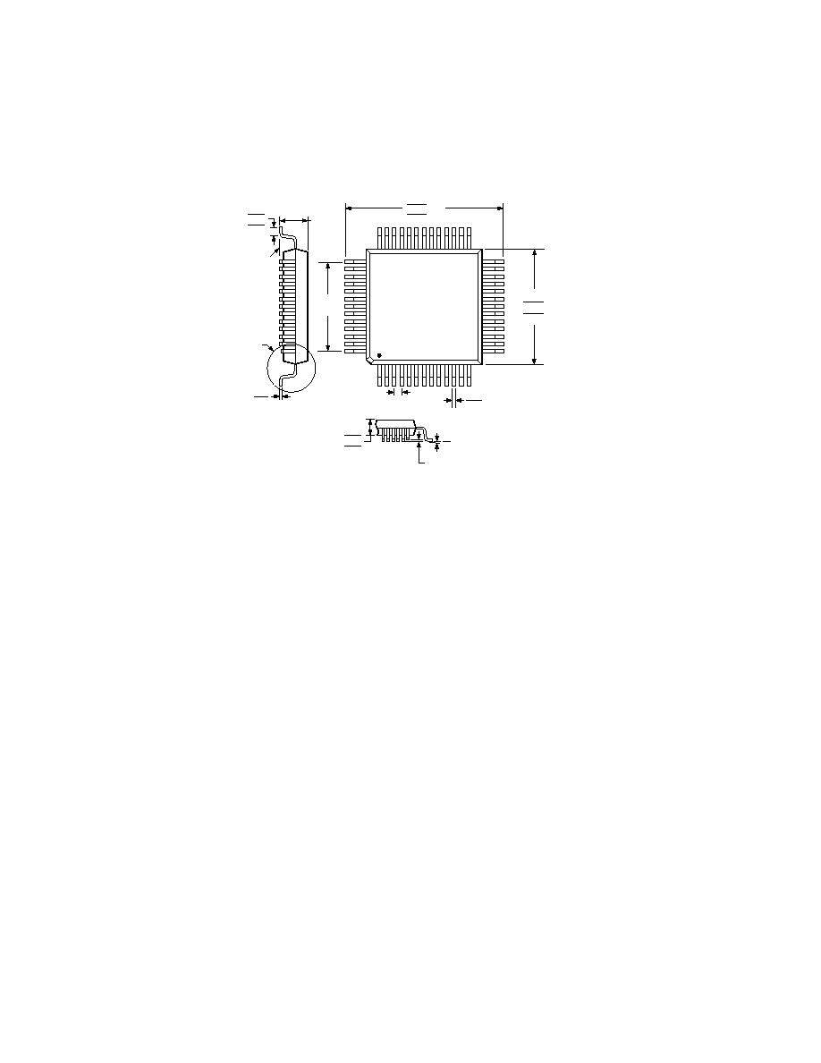
OUTLINE DIMENSIONS
52-Lead Plastic Quad Flatpack [MQFP]
(S-52)
Dimensions shown in millimeters
SEATING
PLANE
VIEW A
0.23
0.11
2.45
MAX
1.03
0.88
0.73
TOP VIEW
(PINS DOWN)
1
39
40
13
14
27
26
52
PIN 1
0.65 BSC
13.45
13.20 SQ
12.95
7.80
REF
10.20
10.00 SQ
9.80
0.40
0.22
VIEW A
ROTATED 90 CCW
7
0
2.20
2.00
1.80
0.13 MIN
COPLANARITY
COMPLIANT TO JEDEC STANDARDS MS-022-AC

REV. B
AD1839
≠23≠
Revision History
Location
Page
8/03--Data Sheet changed from REV. A to REV. B.
Changes to SPECIFICATIONS . . . . . . . . . . . . . . . . . . . . . . . . . . . . . . . . . . . . . . . . . . . . . . . . . . . . . . . . . . . . . . . . . . . . . . . . . . . . 3
Changes to Figure 3 . . . . . . . . . . . . . . . . . . . . . . . . . . . . . . . . . . . . . . . . . . . . . . . . . . . . . . . . . . . . . . . . . . . . . . . . . . . . . . . . . . . . . 13
Replaced Figure 5 . . . . . . . . . . . . . . . . . . . . . . . . . . . . . . . . . . . . . . . . . . . . . . . . . . . . . . . . . . . . . . . . . . . . . . . . . . . . . . . . . . . . . . 14
Changes to Table IV . . . . . . . . . . . . . . . . . . . . . . . . . . . . . . . . . . . . . . . . . . . . . . . . . . . . . . . . . . . . . . . . . . . . . . . . . . . . . . . . . . . . 19
Changes to Table IX . . . . . . . . . . . . . . . . . . . . . . . . . . . . . . . . . . . . . . . . . . . . . . . . . . . . . . . . . . . . . . . . . . . . . . . . . . . . . . . . . . . . 20
Changes to Figure 15 . . . . . . . . . . . . . . . . . . . . . . . . . . . . . . . . . . . . . . . . . . . . . . . . . . . . . . . . . . . . . . . . . . . . . . . . . . . . . . . . . . . . 21
Updated OUTLINE DIMENSIONS . . . . . . . . . . . . . . . . . . . . . . . . . . . . . . . . . . . . . . . . . . . . . . . . . . . . . . . . . . . . . . . . . . . . . . . 22
10/02--Data Sheet changed from REV. 0 to REV. A.
Changes to FUNCTIONAL BLOCK DIAGRAM . . . . . . . . . . . . . . . . . . . . . . . . . . . . . . . . . . . . . . . . . . . . . . . . . . . . . . . . . . . . . . 1
Changes to SPECIFICATIONS . . . . . . . . . . . . . . . . . . . . . . . . . . . . . . . . . . . . . . . . . . . . . . . . . . . . . . . . . . . . . . . . . . . . . . . . . . . . 2
Changes to FUNCTIONAL OVERVIEW section . . . . . . . . . . . . . . . . . . . . . . . . . . . . . . . . . . . . . . . . . . . . . . . . . . . . . . . . . . . . . . 11
Changes to Figure 15 . . . . . . . . . . . . . . . . . . . . . . . . . . . . . . . . . . . . . . . . . . . . . . . . . . . . . . . . . . . . . . . . . . . . . . . . . . . . . . . . . . . . 21
Changes to OUTLINE DIMENSIONS . . . . . . . . . . . . . . . . . . . . . . . . . . . . . . . . . . . . . . . . . . . . . . . . . . . . . . . . . . . . . . . . . . . . . 22

C02955≠0≠8/03(B)
≠24≠


