REV. 0
Information furnished by Analog Devices is believed to be accurate and
reliable. However, no responsibility is assumed by Analog Devices for its
use, nor for any infringements of patents or other rights of third parties
which may result from its use. No license is granted by implication or
otherwise under any patent or patent rights of Analog Devices.
a
AD1881A
One Technology Way, P.O. Box 9106, Norwood, MA 02062-9106, U.S.A.
Tel: 781/329-4700
World Wide Web Site: http://www.analog.com
Fax: 781/326-8703
© Analog Devices, Inc., 2000
AC'97 SoundMAX
Æ
Codec
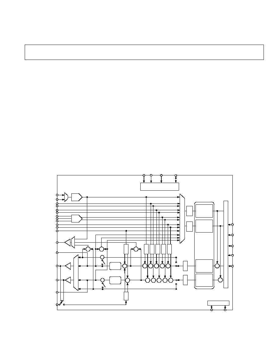
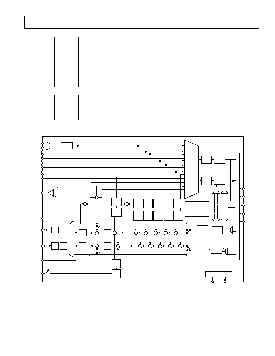
FUNCTIONAL BLOCK DIAGRAM
G
A
M
G
A
M
G
A
M
SYNC
BIT_CLK
PHAT
STEREO
G
A
M
MV
MV
AD1881A
MIC1
MIC2
AUX
CD
VIDEO
LINE_OUT_L
MONO_OUT
LINE_IN
PHONE_IN
LINE_OUT_R
G = GAIN
A = ATTENUATE
M = MUTE
MV = MASTER VOLUME
NC = NO CONNECT
OSCILLATORS
XTL_OUT
XTL_IN
CS1
EAPD
MODE
RESET
SDATA_IN
CS0
MODE/SYNCHRONIZER
SDATA_OUT
G
A
M
G
A
M
G
A
M
16-BIT
D/A
CONVERTER
16-BIT
D/A
CONVERTER
PC_BEEP
PHAT
STEREO
MV
LNLVL_OUT_R
LNLVL_OUT_L
0dB/
20dB
SELECTOR
PGA
PGA
16-BIT
A/D
CONVERTER
16-BIT
A/D
CONVERTER
SAMPLE
RATE
GENERATORS
AC LINK
D
A
M
G
A
M
NC
NC
POP
POP
A
M
AC'97 2.1 FEATURES
Variable Sample Rate
True Line-Level Output
Supports Secondary Codec Modes
AC'97 FEATURES
Designed for AC'97 Analog I/O Component
48-Lead LQFP Package
Multibit
Converter Architecture for Improved
S/N Ratio Greater than 90 dB
16-Bit Stereo Full-Duplex Codec
Four Analog Line-Level Stereo Inputs for Connection
from LINE, CD, VIDEO, and AUX
Two Analog Line-Level Mono Inputs for Speakerphone
and PC BEEP
Mono MIC Input Switchable from Two External
Sources
High Quality CD Input with Ground Sense
Stereo Line-Level Output
Mono Output for Speakerphone or Internal Speaker
Power Management Support
ENHANCED FEATURES
Mobile Low Power Mixer Mode
Digital Audio Mixer Mode
Full Duplex Variable 8 kHz to 48 kHz Sampling Rate
with 1 Hz Resolution
PHATTM Stereo 3D Stereo Enhancement
Split Power Supplies (3.3 V Digital/5 V Analog)
Extended 6-Bit Master Volume Control
Audio Amp Power-Down Signal
SoundMAX is a registered trademark and PHAT is a trademark of Analog Device, Inc.

≠2≠
REV. 0
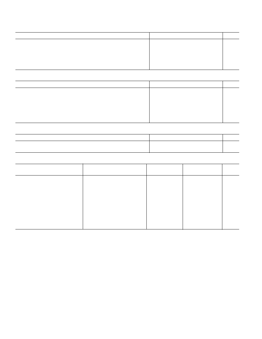
AD1881A≠SPECIFICATIONS
ANALOG INPUT
Parameter
Min
Typ
Max
Unit
Input Voltage (RMS Values Assume Sine Wave Input)
LINE_IN, AUX, CD, VIDEO, PHONE_IN, PC_BEEP
1
V rms
2.83
V p-p
MIC with +20 dB Gain (M20 = 1)
0.1
V rms
0.283
V p-p
MIC with 0 dB Gain (M20 = 0)
1
V rms
2.83
V p-p
Input Impedance
*
20
k
Input Capacitance
*
5
7.5
pF
MASTER VOLUME
Parameter
Min
Typ
Max
Unit
Step Size (0 dB to ≠94.5 dB); LINE_OUT_L, LINE_OUT_R
1.5
dB
Output Attenuation Range Span
*
≠94.5
dB
Step Size (0 dB to ≠46.5 dB); MONO_OUT
1.5
dB
Output Attenuation Range Span
*
≠46.5
dB
Mute Attenuation of 0 dB Fundamental
*
80
dB
PROGRAMMABLE GAIN AMPLIFIER--ADC
Parameter
Min
Typ
Max
Unit
Step Size (0 dB to 22.5 dB)
1.5
dB
PGA Gain Range Span
22.5
dB
ANALOG MIXER--INPUT GAIN/AMPLIFIERS/ATTENUATORS
Parameter
Min
Typ
Max
Unit
Signal-to-Noise Ratio (SNR)
CD to LINE_OUT
90
dB
Other to LINE_OUT
90
dB
Step Size (+12 dB to ≠34.5 dB): (All Steps Tested)
MIC, LINE_IN, AUX, CD, VIDEO, PHONE_IN, DAC
1.5
dB
Input Gain/Attenuation Range: MIC, LINE, AUX, CD, VIDEO, PHONE_IN, DAC
≠46.5
dB
Step Size (0 dB to ≠45 dB): (All Steps Tested) PC_BEEP
3.0
dB
Input Gain/Attenuation Range: PC_BEEP
≠45
dB
*Guaranteed, not tested.
Specifications subject to change without notice.
Temperature
25
∞C
Digital Supply (V
DD
)
3.3
V
Analog Supply (V
CC
)
5.0
V
Sample Rate (F
S
)
48
kHz
Input Signal
1008
Hz
STANDARD TEST CONDITIONS UNLESS OTHERWISE NOTED
DAC Test Conditions
Calibrated
≠3 dB Attenuation Relative to Full-Scale
Input 0 dB
10 k
Output Load
ADC Test Conditions
Calibrated
0 dB Gain
Input ≠3.0 dB Relative to Full-Scale

≠3≠
REV. 0
AD1881A
DIGITAL DECIMATION AND INTERPOLATION FILTERS
*
Parameter
Min
Typ
Max
Unit
Passband
0
0.4
◊ F
S
Hz
Passband Ripple
±0.09
dB
Transition Band
0.4
◊ F
S
0.6
◊ F
S
Hz
Stopband
0.6
◊ F
S
Hz
Stopband Rejection
≠74
dB
Group Delay
12/F
S
sec
Group Delay Variation Over Passband
0.0
µs
ANALOG-TO-DIGITAL CONVERTERS
Parameter
Min
Typ
Max
Unit
Resolution
16
Bits
Total Harmonic Distortion (THD)
0.02
%
≠74
dB
Dynamic Range (≠60 dB Input THD+N Referenced to Full Scale, A-Weighted)
87
dB
Signal-to-Intermodulation Distortion
* (CCIF Method)
85
dB
ADC Crosstalk
*
Line Inputs (Input L, Ground R, Read R; Input R, Ground L, Read L)
≠100
≠90
dB
LINE_IN to Other
≠90
≠85
dB
Gain Error (Full-Scale Span Relative to Nominal Input Voltage)
±10
%
Interchannel Gain Mismatch (Difference of Gain Errors)
±0.5
dB
ADC Offset Error
±10.5
mV
DIGITAL-TO-ANALOG CONVERTERS
Parameter
Min
Typ
Max
Unit
Resolution
16
Bits
Total Harmonic Distortion (THD) LINE_OUT, LNLVL_OUT
0.02
%
≠74
dB
Dynamic Range (≠60 dB Input THD+N Referenced to Full Scale, A-Weighted)
90
dB
Signal-to-Intermodulation Distortion
* (CCIF Method)
85
dB
Gain Error (Full-Scale Span Relative to Nominal Input Voltage)
±10
%
Interchannel Gain Mismatch (Difference of Gain Errors)
±0.7
dB
DAC Crosstalk
* (Input L, Zero R, Measure R_OUT; Input R, Zero L,
≠80
dB
Measure L_OUT)
Total Audible Out-of-Band Energy (Measured from 0.6
◊ F
S
to 20 kHz)
*
≠40
dB
ANALOG OUTPUT
Parameter
Min
Typ
Max
Unit
Full-Scale Output Voltage
1
V rms
(LINE_OUT, LNLVL_OUT)
2.83
V p-p
Output Impedance
*
500
External Load Impedance
*
10
k
Output Capacitance
*
15
pF
External Load Capacitance
100
pF
V
REF
2.0
2.2
2.5
V
V
REF_OUT
2.2
V
Mute Click (Muted Output Minus Unmuted Midscale DAC Output)
±5
mV
*Guaranteed, not tested.
Specifications subject to change without notice.
≠4≠
REV. 0
AD1881A≠SPECIFICATIONS
STATIC DIGITAL SPECIFICATIONS
Parameter
Min
Typ
Max
Unit
High Level Input Voltage (V
IH
): Digital Inputs
0.65
◊ DV
DD
V
Low Level Input Voltage (V
IL
)
0.35
◊ DV
DD
V
High Level Output Voltage (V
OH
), I
OH
= ≠0.5 mA
0.9
◊ DV
DD
V
Low Level Output Voltage (V
OL
), I
OL
= +0.5 mA
0.1
◊ DV
DD
V
Input Leakage Current
≠10
+10
µA
Output Leakage Current
≠10
+10
µA
POWER SUPPLY
Parameter
Min
Typ
Max
Unit
Power Supply Range ≠ Analog
4.75
5.25
V
Power Supply Range ≠ Digital (3.3 V)
3.0
3.6
V
Power Dissipation ≠ 5 V/3.3 V
280
mW
Analog Supply Current ≠ 5 V
40
mA
Digital Supply Current ≠ 3.3 V
23
mA
Power Supply Rejection (100 mV p-p Signal @ 1 kHz)
*
40
dB
(At Both Analog and Digital Supply Pins, Both ADCs and DACs)
CLOCK SPECIFICATIONS
*
Parameter
Min
Typ
Max
Unit
Input Clock Frequency
24.576
MHz
Recommended Clock Duty Cycle
45
50
55
%
POWER-DOWN MODE
DV
DD
(3.3 V)
AV
DD
(5 V)
Parameter
Set Bits
Typ
Typ
Unit
ADC
PR0
17
30
mA
DAC
PR1
17
26
mA
ADC and DAC
PR1, PR0
4
20
mA
ADC + DAC + Mixer (Analog CD On) LPMIX, PR1, PR0
4
12
mA
Mixer
PR2
20
18
mA
ADC + Mixer
PR2, PR0
17
12
mA
DAC + Mixer
PR2, PR1
17
8
mA
ADC + DAC + Mixer
PR2, PR1, PR0
4
2
mA
Analog CD Only (AC-Link On)
LPMIX, PR5, PR1, PR0
4
12
mA
Analog CD Only (AC-Link Off)
LPMIX, PR1, PR0, PR4, PR5
0
12
mA
Standby
PR5, PR4, PR3, PR2, PR1, PR0
0
0.1
mA
*Guaranteed, not tested.
Specifications subject to change without notice.

AD1881A
≠5≠
REV. 0
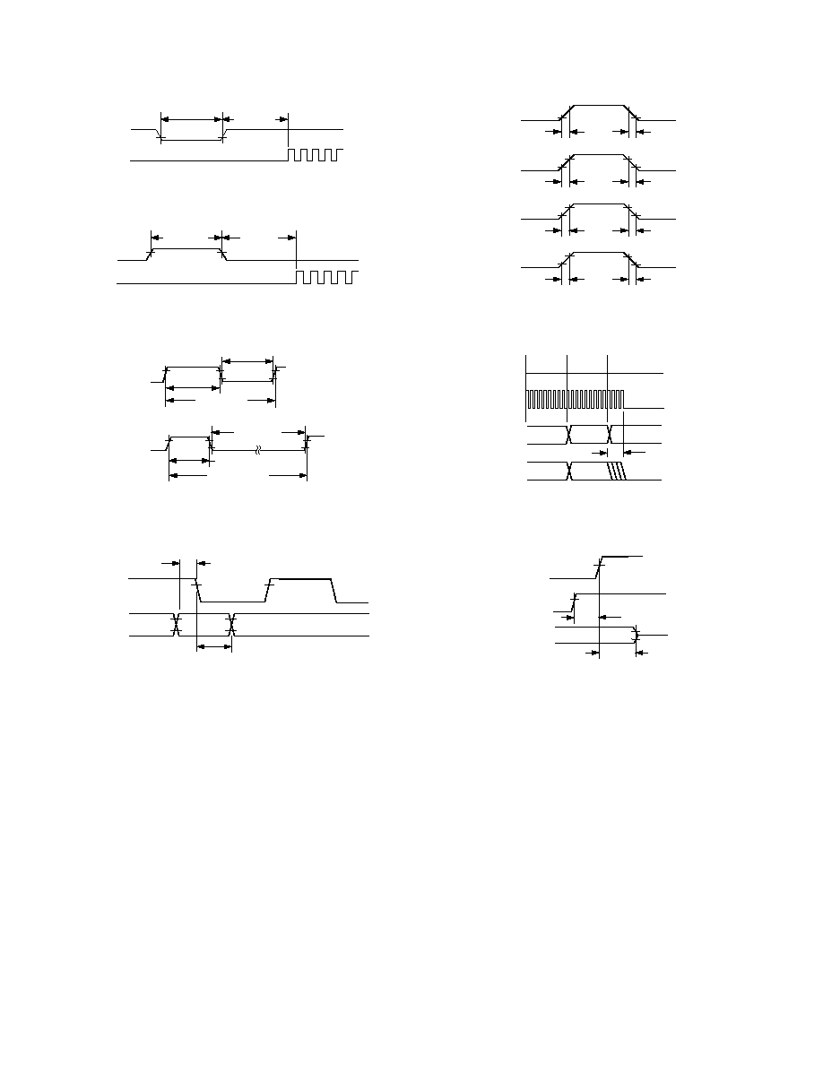
TIMING PARAMETERS
1
(GUARANTEED OVER OPERATING TEMPERATURE RANGE)
Parameter
Symbol
Min
Typ
Max
Unit
RESET Active Low Pulsewidth
t
RST_LOW
50
ns
RESET Inactive to BIT_CLK Startup Delay
t
RST2CLK
833
µs
SYNC Active High Pulsewidth
t
SYNC_HIGH
80
ns
SYNC Low Pulsewidth
t
SYNC_LOW
19.5
µs
SYNC Inactive to BIT_CLK Startup Delay
t
SYNC2CLK
162.8
ns
BIT_CLK Frequency
12.288
MHz
BIT_CLK Period
t
CLK_PERIOD
81.4
ns
BIT_CLK Output Jitter
2
750
ps
BIT_CLK High Pulsewidth
t
CLK_HIGH
36.62
40.69
44.76
ns
BIT_CLK Low Pulsewidth
t
CLK_LOW
36.62
40.69
44.76
ns
SYNC Frequency
48.0
kHz
SYNC Period
t
SYNC_PERIOD
20.8
µs
Setup to Falling Edge of BIT_CLK
t
SETUP
5
2.5
ns
Hold from Falling Edge of BIT_CLK
t
HOLD
5
ns
BIT_CLK Rise Time
t
RISECLK
2
4
10
ns
BIT_CLK Fall Time
t
FALLCLK
2
4
10
ns
SYNC Rise Time
t
RISESYNC
2
4
10
ns
SYNC Fall Time
t
FALLSYNC
2
4
10
ns
SDATA_IN Rise Time
t
RISEDIN
2
4
10
ns
SDATA_IN Fall Time
t
FALLDIN
2
4
10
ns
SDATA_OUT Rise Time
t
RISEDOUT
2
4
10
ns
SDATA_OUT Fall Time
t
FALLDOUT
2
4
10
ns
End of Slot 2 to BIT_CLK, SDATA_IN Low
t
S2_PDOWN
0
10
ms
Setup to Trailing Edge of
RESET (Applies to SYNC, SDATA_OUT)
t
SETUP2RST
15
ns
Rising Edge of
RESET to HI-Z Delay (ATE Test Mode)
t
OFF
25
ns
Propagation Delay
15
ns
RESET Rise Time
50
ns
NOTES
1
Guaranteed, not tested.
2
Output jitter is directly dependent on crystal input jitter.
Specifications subject to change without notice.
AD1881A
≠6≠
REV. 0
RESET
BIT_CLK
t
RST2CLK
t
RST_LOW
Figure 1. Cold Reset
SYNC
BIT_CLK
t
SYNC_HIGH
t
RST2CLK
Figure 2. Warm Reset
t
CLK_HIGH
BIT_CLK
t
CLK_LOW
SYNC
t
SYNC_HIGH
t
SYNC_LOW
t
SYNC_PERIOD
t
CLK_PERIOD
Figure 3. Clock Timing
BIT_CLK
SYNC
t
HOLD
SDATA_OUT
t
SETUP
Figure 4. Data Setup and Hold
BIT_CLK
SYNC
SDATA_IN
t
RISECLK
t
RISESYNC
t
RISEDIN
t
RISEDOUT
t
FALLCLK
t
FALLSYNC
t
FALLDIN
t
FALLDOUT
SDATA_OUT
Figure 5. Signal Rise and Fall Time
BIT_CLK
SDATA_OUT
SYNC
SDATA_IN
SLOT 1
SLOT 2
WRITE
TO 0x26
DATA
PR4
DON'T
CARE
t
S2_PDOWN
NOTE: BIT_CLK NOT TO SCALE
Figure 6. AC Link Low Power Mode Timing
RESET
SDATA_OUT
HI-Z
t
SETUP2RST
t
OFF
SDATA_IN, BIT_CLK
Figure 7. ATE Test Mode
AD1881A
≠7≠
REV. 0
ABSOLUTE MAXIMUM RATINGS
*
Parameter
Min
Max
Unit
Power Supplies
Digital (V
DD
)
≠0.3
+3.6
V
Analog (V
CC
)
≠0.3
+6.0
V
Analog Input Voltage (Signal Pins)
≠0.3
V
CC
+ 0.3
V
Digital Input Voltage (Signal Pins)
≠0.3
V
DD
+ 0.3
V
Ambient Temperature (Operating)
0
+70
∞C
Storage Temperature
≠65
+150
∞C
*Stresses greater than those listed under Absolute Maximum Ratings may cause
permanent damage to the device. This is a stress rating only; functional operation
of the device at these or any other conditions above those indicated in t he
operational section of this specification is not implied. Exposure to absolute maximum
rating conditions for extended periods may affect device reliability.
ORDERING GUIDE
Temperature
Package
Package
Model
Range
Description
Option
AD1881AJST 0
∞C to 70∞C
48-Lead LQFP
ST-48
ENVIRONMENTAL CONDITIONS
Ambient Temperature Rating
T
AMB
= T
CASE
≠ (PD
◊
CA
)
T
CASE
= Case Temperature in
∞C
P
D
= Power Dissipation in W
CA
= Thermal Resistance (Case-to-Ambient)
JA
= Thermal Resistance (Junction-to-Ambient)
JC
= Thermal Resistance (Junction-to-Case)
Package
JA
JC
CA
LQFP
76.2
∞C/W
17
∞C/W
59.2
∞C/W
CAUTION
ESD (electrostatic discharge) sensitive device. Electrostatic charges as high as 4000 V readily
accumulate on the human body and test equipment and can discharge without detection. Although
the AD1881A features proprietary ESD protection circuitry, permanent damage may occur on
devices subjected to high-energy electrostatic discharges. Therefore, proper ESD precautions are
recommended to avoid performance degradation or loss of functionality.
WARNING!
ESD SENSITIVE DEVICE
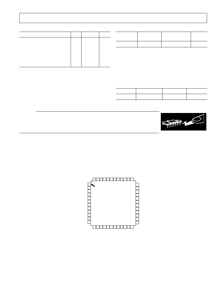
PIN CONFIGURATION
48-Lead LQFP
36
35
34
33
32
31
30
29
28
27
26
25
13 14 15 16 17 18 19 20 21 22 23 24
AV
SS2
EAPD/CHAIN_IN
LNLVL_OUT_R
CS0
NC
NC
NC
1
2
3
4
5
6
7
8
9
10
11
12
48 47 46 45 44
39 38 37
43 42 41 40
PIN 1
IDENTIFIER
TOP VIEW
(Not to Scale)
LINE_OUT_R
LINE_OUT_L
CX3D
RX3D
FILT_L
FILT_R
AFILT2
PHONE_IN
AUX_L
AUX_R
VIDEO_L
CD_GND_REF
DV
DD1
XTL_IN
XTL_OUT
SDATA_OUT
BIT_CLK
SDATA_IN
SYNC
RESET
PC_BEEP
NC = NO CONNECT
AFILT1
CD_R
MIC1
MIC2
LINE_IN_L
MONO_OUT
AD1881A
LINE_IN_R
CS1
CD_L
VIDEO_R
MODE
DV
SS1
DV
SS2
DV
DD2
VREFOUT
VREF
AV
SS1
AV
DD1
AV
DD2
LNLVL_OUT_L

AD1881A
≠8≠
REV. 0
PIN FUNCTION DESCRIPTIONS
Digital I/O
Pin Name
LQFP
I/O
Description
XTL_IN
2
I
Crystal (or Clock) Input, 24.576 MHz.
XTL_OUT
3
O
Crystal Output.
SDATA_OUT
5
I
AC-Link Serial Data Output, AD1881A Input Stream.
BIT_CLK
6
O
AC-Link Bit Clock. 12.288 MHz Serial Data Clock. Daisy Chain Output Clock.
SDATA_IN
8
O
AC-Link Serial Data Input. AD1881A Output Stream.
SYNC
10
I
AC-Link Frame Sample Sync 48 kHz Fixed Rate.
RESET
11
I
AC-Link Reset. AD1881A Master H/W Reset.
Miscellaneous Connections
Pin Name
LQFP
I/O
Description
CS0
45
I
Chip Select 0.
CS1
46
I
Chip Select 1.
EAPD
47
O
External Amp Power-Down Control Signal, Default LO, Active HI
MODE
48
I
MODE Select.
Analog I/O
These signals connect the AD1881A component to analog sources and sinks, including microphones and speakers.
Pin Name
LQFP
I/O
Description
PC_BEEP
12
I
PC Beep. PC Speaker Beep Passthrough.
PHONE_IN
13
I
Phone. From Telephony Subsystem Speakerphone or Handset.
AUX_L
14
I
Auxiliary Input Left Channel.
AUX_R
15
I
Auxiliary Input Right Channel.
VIDEO_L
16
I
Video Audio Left Channel.
VIDEO_R
17
I
Video Audio Right Channel.
CD_L
18
I
CD Audio Left Channel.
CD_GND_REF
19
I
CD Audio Analog Ground Reference for Pseudo-Differential CD Input.
CD_ R
20
I
CD Audio Right Channel.
MIC1
21
I
Microphone 1. Desktop Microphone Input.
MIC2
22
I
Microphone 2. Second Microphone Input.
LINE_IN_L
23
I
Line In Left Channel.
LINE_IN_R
24
I
Line In Right Channel.
LINE_OUT_L
35
O
Line Out Left Channel.
LINE_OUT_R
36
O
Line Out Right Channel.
MONO_OUT
37
O
Monaural Output to Telephony Subsystem Speakerphone.
LNLVL_OUT_L
39
O
Line-Level Output Left Channel.
LNLVL_OUT_R
41
O
Line-Level Output Right Channel.
Filter/Reference
These signals are connected to resistors, capacitors, or specific voltages.
Pin Name
LQFP
I/O
Description
VREF
27
O
Voltage Reference Filter.
VREFOUT
28
O
Voltage Reference Output 5 mA Drive (Intended for MIC Bias).
AFILT1
29
O
Antialiasing Filter Capacitor--ADC Right Channel.
AFILT2
30
O
Antialiasing Filter Capacitor--ADC Left Channel.
FILT_R
31
O
AC-Coupling Filter Capacitor--ADC Right Channel.
FILT_L
32
O
AC-Coupling Filter Capacitor--ADC Left Channel.
RX3D
33
O
3D PHAT Stereo Enhancement--Capacitor.
CX3D
34
I
3D PHAT Stereo Enhancement--Capacitor.
AD1881A
≠9≠
REV. 0
Power and Ground Signals
Pin Name
LQFP
Type
Description
DV
DD1
1
I
Digital V
DD
3.3 V
DV
SS1
4
I
Digital GND
DV
SS2
7
I
Digital GND
DV
DD2
9
I
Digital V
DD
3.3 V
AV
DD1
25
I
Analog V
DD
5.0 V
AV
SS1
26
I
Analog GND
AV
DD2
38
I
Analog V
DD
5.0 V
AV
SS2
42
I
Analog GND
No Connects
Pin Name
LQFP
Type
Description
NC
40
No Connect
NC
43
No Connect
NC
44
No Connect
0x20
PHAT
0x22
DP
0
X
74
OSCILLATORS
G = GAIN
A = ATTENUATE
M = MUTE
MV = MASTER VOLUME
GM 0x1C
RIM
IM
GM 0x1C
LIM
IM
LS/RS (0)
LS (4)
RS (4)
LS (3)
RS (3)
LS (1)
RS (1)
LS/RS (6)
RS (5)
LS (2)
RS (2)
S 0x1A
S
E
L
E
C
T
O
R
LS/RS (7)
LS (5)
0x20
POP
M 0x14
VM
M 0x16
CM
M 0x12
AM
M 0x10
LM
M 0x0E
MCM
RESET
SYNC
BIT_CLK
SDATA_OUT
SDATA_IN
GM 0
X
1C
LIM
IM
GA 0x14
LVV
RVV
GA 0x12
LCV
RCV
GA 0x16
LAV
RAV
GA 0x10
LLV
RLA
GA 0x0E
MCV
GAM 0x18
LOV
OM
ROV
OM
GAM 0x18
AC LINK
GM 0
X
1C
RIM
IM
16-BIT
A/D
16-BIT
A/D
16-BIT
D/A
16-BIT
D/A
LPBK
0x20
PCM DAC RATE 0x2C
SR1
0x7A
PCM ADC RATE 0x32
SR0
0x78
XTL_OUT
XTL_IN
STEREO MIX (L)
MONO MIX
STEREO MIX (R)
AD1881A
M 0x0C
PHM
GA 0x0C
PHV
A 0x0A
PCV
M 0x0A
PCM
0x02
MM
0x20
0x02
MM
MS
0
1
DAM
02
LMV
LINE_OUT_L
LINE_OUT_R
PC_BEEP
MIC1
MIC2
AUX
CD
VIDEO
0dB/20dB
M20 0x0E
PHONE_IN
LINE_IN
LNLVL_OUT_L
LNLVL_OUT_R
02
LMV
0x22
DP
MV
NC
NC
MIX
0x20
0x20
PHAT
POP
0x20
POP
0x20
MONO_OUT
Figure 8. Block Diagram Register Map

AD1881A
≠10≠
REV. 0
PRODUCT OVERVIEW
The AD1881A meets the Audio Codec '97 2.0 and 2.1 Extensions. In
addition, the AD1881A SoundMAX Codec is designed to meet all
requirements of the Audio Codec '97, Component Specification, Revi-
sion 1.03, © 1996, Intel Corporation, found at www.Intel.com.
The AD1881A also includes some other Codec enhanced fea-
tures such as the built-in PHAT Stereo 3D enhancement.
The AD1881A is an analog front end for high performance PC
audio applications. The AC'97 architecture defines a 2-chip
audio solution comprising a digital audio controller, plus a high
quality analog component that includes Digital-to-Analog
Converters (DACs), Analog-to-Digital Converters (ADCs),
mixer and I/O.
The main architectural features of the AD1881A are the high
quality analog mixer section, two channels of
ADC conversion,
two channels of
DAC conversion with Data Direct Scram-
bling (D
2
S) rate generators. The AD1881A's left channel ADC
and DAC are compatible for modem applications supporting irra-
tional sample rates and modem filtering requirements.
FUNCTIONAL DESCRIPTION
This section overviews the functionality of the AD1881A and
is intended as a general introduction to the capabilities of the
device. Detailed reference information may be found in the
descriptions of the Indexed Control Registers.
Analog Inputs
The Codec contains a stereo pair of
ADCs. Inputs to the
ADC may be selected from the following analog signals: tele-
phony (PHONE_IN), mono microphone (MIC1 or MIC2),
stereo line (LINE_IN), auxiliary line input (AUX), stereo CD
ROM (CD), stereo audio from a video source (VIDEO) and
post-mixed stereo or mono line output (LINE_OUT).
Analog Mixing
PHONE_IN, MIC1 or MIC2, LINE_IN, AUX, CD and VIDEO
can be mixed in the analog domain with the stereo output from the
DACs. Each channel of the stereo analog inputs may be inde-
pendently gained or attenuated from +12 dB to ≠34.5 dB in 1.5 dB
steps. The summing path for the mono inputs (PHONE_IN, MIC1,
and MIC2 to LINE_OUT) duplicates mono channel data on both
the left and right LINE_OUT. Additionally, the PC attention sig-
nal (PC_BEEP) may be mixed with the line output. A switch
allows the output of the DACs to bypass the PHAT Stereo
3D enhancement.
Digital Audio Mode
The AD1881A is designed with a Digital Audio Mode (DAM)
that allows mixing of all analog inputs independent of the DAC
output signal path. Mixed analog input signals may be sent to
the ADCs for processing by the controller or the host, and may
be used during simultaneous capture and playback at different
sample rates.
Analog-to-Digital Signal Path
The selector sends left and right channel information to the
programmable gain amplifier (PGA). The PGA following the
selector allows independent gain control for each channel entering
the ADC from 0 dB to +22.5 dB in 1.5 dB steps. Each channel
of the ADC is independent, and can process left and right chan-
nel data at different sample rates.
Sample Rates and D
2
S
The AD1881A default mode sets the Codec to operate at 48 kHz
sample rates. The converter pairs may process left and right
channel data at different sample rates. The AD1881A sample
rate generator allows the Codec to instantaneously change and
process sample rates from 8 kHz to 48 kHz with a resolution
of 1 Hz. The in-band integrated noise and distortion artifacts
introduced by rate conversions are below ≠90 dB. The AD1881A
uses a 4-bit D/A structure and Data Directed Scrambling (D
2
S)
to enhance noise immunity on motherboards and in PC enclo-
sures, and to suppress idle tones below the device's quantization
noise floor. The D
2
S process pushes noise and distortion artifacts
caused by errors in the multibit DAC to frequencies beyond the
auditory response of the human ear and then filters them.
Digital-to-Analog Signal Path
The analog output of the DAC may be gained or attenuated from
+12 dB to ≠34.5 dB in 1.5 dB steps, and summed with any of
the analog input signals. The summed analog signal enters the
Master Volume stage where each channel of the mixer output may
be attenuated from 0 dB to ≠94.5 dB in 1.5 dB steps or muted.
Line-Level Outputs
The AD1881A offers a true line-level output for notebook dock-
ing station and home theater applications. The line-level output
does not change with master volume settings.
Host-Based Echo Cancellation Support
The AD1881A supports time correlated I/O data format by pre-
senting MIC data on the left channel of the ADC and the mono
summation of left and right output on the right channel. The
ADC is splittable; left and right ADC data can be sampled at
different rates.
Power Management Modes
The AD1881A is designed to meet ACPI power consumption
requirements through flexible power management control of all
internal resources.

AD1881A
≠11≠
REV. 0
Indexed Control Registers
Reg
Num
Name
D15
D14
D13
D12
D11
D10
D9
D8
D7
D6
D5
D4
D3
D2
D1
D0
Default
00h
Reset
X
SE4
SE3
SE2
SE1
SE0
ID9
ID8
ID7
ID6
ID5
ID4
ID3
ID2
ID1
ID0
0410h
02h
Master Volume
MM
X
LMV5 LMV4 LMV3 LMV2 LMV1 LMV0 X
X
RMV5 RMV4 RMV3 RMV2 RMV1 RMV0
8000h
04h
Reserved
X
X
X
X
X
X
X
X
X
X
X
X
X
X
X
X
X
06h
Master Volume Mono
MMM
X
X
X
X
X
X
X
X
X
X
MMV MMV MMV MMV MMV
8000h
4
2
2
1
0
08h
Reserved
X
X
X
X
X
X
X
X
X
X
X
X
X
X
X
X
X
0Ah
PC Beep Volume
PCM
X
X
X
X
X
X
X
X
X
X
PCV3
PCV2
PCV1
PCV0
X
8000h
0Ch
Phone In Volume
PHM
X
X
X
X
X
X
X
X
X
X
PHV4 PHV3 PHV2 PHV1 PHV0
8008h
0Eh
MIC Volume
MCM
X
X
X
X
X
X
X
X
M20
X
MCV4 MCV3 MCV2 MCV1 MCV0 8008h
10h
Line In Volume
LM
X
X
LLV4
LLV3
LLV2
LLV1
LLV0
X
X
X
RLV4
RLV3
RLV2
RLV1
RLV0
8808h
12h
CD Volume
CVM
X
X
LCV4 LCV3 LCV2 LCV1 LCV0 X
X
X
RCV4 RCV3 RCV2 RCV1 RCV0
8808h
14h
Video Volume
VM
X
X
LVV4
LVV3
LVV2
LVV1
LVV0
X
X
X
RVV4
RVV3
RVV2
RVV1
RVV0
8808h
16h
Aux Volume
AM
X
X
LAV4
LAV3
LAV2
LAV1
LAV0
X
X
X
RAV4 RAV3 RAV2 RAV1 RAV0
8808h
18h
PCM Out Vol
OM
X
X
LOV4 LOV3 LOV2 LOV1 LOV0 X
X
X
ROV4 ROV3 ROV2 ROV1 ROV0
8808h
1Ah
Record Select
X
X
X
X
X
LS2
LS1
LS0
X
X
X
X
X
RS2
RS1
RS0
0000h
1Ch
Record Gain
IM
X
X
X
LIM3
LIM2
LIM1
LIM0
X
X
X
X
RIM3
RIM2
RIM1
RIM0
8000h
1Eh
Reserved
X
X
X
X
X
X
X
X
X
X
X
X
X
X
X
X
X
20h
General Purpose
POP
X
3D
X
X
X
MIX
MS
LPBK X
X
X
X
X
X
X
0000h
22h
3D Control
X
X
X
X
X
X
X
X
X
X
X
X
DP3
DP2
DP1
DP0
0000h
26h
Power-Down Cntrl/Stat
EAPD
X
PR5
PR4
PR3
PR2
PR1
PR0
X
X
X
X
REF
ANL
DAC
ADC
000Xh
28h
Extended Audio ID
ID1
ID0
X
X
X
X
X
X
X
X
X
X
X
X
X
VRA
0001h
2Ah
Extended Audio Stat/Ctrl
X
X
X
X
X
X
X
X
X
X
X
X
X
X
X
VRA
0000h
2Ch/
PCM DAC Rate (SR1)
SR15
SR14
SR13
SR12
SR11
SR10
SR9
SR8
SR7
SR6
SR5
SR4
SR3
SR2
SR1
SR0
BB80h
(7Ah)
*
32h /
PCM ADC Rate (SR0)
SR15
SR14
SR13
SR12
SR11
SR10
SR9
SR8
SR7
SR6
SR5
SR4
SR3
SR2
SR1
SR0
BB80h
(78h)
*
34h
Reserved
X
X
X
X
X
X
X
X
X
X
X
X
X
X
X
X
X
5ah
Vendor Reserved
**
..
..
..
..
..
..
..
..
..
..
..
..
..
..
..
..
..
70h
72h
Reserved
X
X
X
X
X
X
X
X
X
X
X
X
X
X
X
X
X
74h
Serial Configuration
SLOT
X
X
X
X
X
X
X
X
X
X
X
X
X
X
X
7X0Xh
16
76h
Misc. Control Bits
DAC
LPMI X
DAM
DMS
DLSR X
ALSR MOD
SRX
SRX
X
X
DRSR X
ARSR
0404h
Z
X
EN
10D7
8D7
7Ch
Vendor ID1
F7
F6
F5
F4
F3
F2
F1
F0
S7
S6
S5
S4
S3
S2
S1
S0
4144h
7Eh
Vendor ID2
T7
T6
T5
T4
T3
T2
T1
T0
REV7
REV6
REV5
REV4
REV3
REV2
REV1
REV0
5348h
NOTES
All registers not shown and bits containing an X are assumed to be reserved.
Odd register addresses are aliased to the next lower even address.
Reserved registers should not be written.
Zeros should be written to reserved bits.
*Indicates Aliased register for AD1819, AD1819A backward compatibility.
**Vendor Reserved registers should not be written.
AD1881A
≠12≠
REV. 0
Reset (Index 00h)
g
e
R g
e
R g
e
R g
e
R g
e
R
m
u
N m
u
N m
u
N m
u
N m
u
N
e
m
a
N
e
m
a
N
e
m
a
N
e
m
a
N
e
m
a
N
5
1
D 5
1
D 5
1
D 5
1
D 5
1
D
4
1
D 4
1
D 4
1
D 4
1
D 4
1
D
3
1
D 3
1
D 3
1
D 3
1
D 3
1
D
2
1
D 2
1
D 2
1
D 2
1
D 2
1
D
1
1
D 1
1
D 1
1
D 1
1
D 1
1
D
0
1
D 0
1
D 0
1
D 0
1
D 0
1
D
9
D9
D9
D9
D9
D
8
D8
D8
D8
D8
D
7
D7
D7
D7
D7
D
6
D6
D6
D6
D6
D
5
D5
D5
D5
D5
D
4
D4
D4
D4
D4
D
3
D3
D3
D3
D3
D
2
D2
D2
D2
D2
D
1
D1
D1
D1
D1
D
0
D0
D0
D0
D0
D
t
l
u
a
f
e
D
t
l
u
a
f
e
D
t
l
u
a
f
e
D
t
l
u
a
f
e
D
t
l
u
a
f
e
D
h
0
0 h
0
0 h
0
0 h
0
0 h
0
0
t
e
s
e
R
t
e
s
e
R
t
e
s
e
R
t
e
s
e
R
t
e
s
e
R
X
X
X
X
X
4
E
S 4
E
S 4
E
S 4
E
S 4
E
S
3
E
S 3
E
S 3
E
S 3
E
S 3
E
S
2
E
S 2
E
S 2
E
S 2
E
S 2
E
S
1
E
S 1
E
S 1
E
S 1
E
S 1
E
S
0
E
S 0
E
S 0
E
S 0
E
S 0
E
S
9
D
I 9
D
I 9
D
I 9
D
I
9
D
I
8
D
I 8
D
I 8
D
I 8
D
I
8
D
I
7
D
I 7
D
I 7
D
I 7
D
I
7
D
I
6
D
I 6
D
I 6
D
I 6
D
I
6
D
I
5
D
I 5
D
I 5
D
I 5
D
I
5
D
I
4
D
I 4
D
I 4
D
I 4
D
I
4
D
I
3
D
I 3
D
I 3
D
I 3
D
I
3
D
I
2
D
I 2
D
I 2
D
I 2
D
I
2
D
I
1
D
I 1
D
I 1
D
I 1
D
I
1
D
I
0
D
I 0
D
I 0
D
I 0
D
I
0
D
I
h
0
1
4
0
h
0
1
4
0
h
0
1
4
0
h
0
1
4
0
h
0
1
4
0
Note: Writing any value to this register performs a register reset, which causes all registers to revert to their default values (except
74h, which forces the serial configuration). Reading this register returns the ID code of the part and a code for the type of 3D Stereo
Enhancement.
ID[9:0]
Identify Capability. The ID decodes the capabilities of AD1881A based on the following:
Bit = 1
Function
AD1881A
ID0
Dedicated MIC PCM In Channel
0
ID1
Modem Line Codec Support
0
ID2
Bass and Treble Control
0
ID3
Simulated Stereo (Mono to Stereo)
0
ID4
Headphone Out/True Line-Level Out
1
ID5
Loudness (Bass Boost) Support
0
ID6
18-Bit DAC Resolution
0
ID7
20-Bit DAC Resolution
0
ID8
18-Bit ADC Resolution
0
ID9
20-Bit ADC Resolution
0
SE[4:0]
Stereo Enhancement. The 3D stereo enhancement identifies the Analog Devices 3D stereo enhancement.
Master Volume Registers (Index 02h)
g
e
R g
e
R g
e
R g
e
R g
e
R
m
u
N m
u
N m
u
N m
u
N m
u
N
e
m
a
N
e
m
a
N
e
m
a
N
e
m
a
N
e
m
a
N
5
1
D 5
1
D 5
1
D 5
1
D 5
1
D
4
1
D 4
1
D 4
1
D 4
1
D 4
1
D
3
1
D 3
1
D 3
1
D 3
1
D 3
1
D
2
1
D 2
1
D 2
1
D 2
1
D 2
1
D
1
1
D 1
1
D 1
1
D 1
1
D 1
1
D
0
1
D 0
1
D 0
1
D 0
1
D 0
1
D
9
D9
D9
D9
D9
D
8
D8
D8
D8
D8
D
7
D7
D7
D7
D7
D
6
D6
D6
D6
D6
D
5
D5
D5
D5
D5
D
4
D4
D4
D4
D4
D
3
D3
D3
D3
D3
D
2
D2
D2
D2
D2
D
1
D1
D1
D1
D1
D
0
D0
D0
D0
D0
D
t
l
u
a
f
e
D
t
l
u
a
f
e
D
t
l
u
a
f
e
D
t
l
u
a
f
e
D
t
l
u
a
f
e
D
h
2
0 h
2
0 h
2
0 h
2
0 h
2
0
r
e
t
s
a
M
r
e
t
s
a
M
r
e
t
s
a
M
r
e
t
s
a
M
r
e
t
s
a
M
e
m
u
l
o
V
e
m
u
l
o
V
e
m
u
l
o
V
e
m
u
l
o
V
e
m
u
l
o
V
M
MM
MM
MM
MM
M
X
X
X
X
X
5
V
M
L
5
V
M
L
5
V
M
L
5
V
M
L
5
V
M
L
4
V
M
L
4
V
M
L
4
V
M
L
4
V
M
L
4
V
M
L
3
V
M
L
3
V
M
L
3
V
M
L
3
V
M
L
3
V
M
L
2
V
M
L
2
V
M
L
2
V
M
L
2
V
M
L
2
V
M
L
1
V
M
L
1
V
M
L
1
V
M
L
1
V
M
L
1
V
M
L
0
V
M
L
0
V
M
L
0
V
M
L
0
V
M
L
0
V
M
L
X
X
X
X
X
X
X
X
X
X
5
V
M
R
5
V
M
R
5
V
M
R
5
V
M
R
5
V
M
R
4
V
M
R
4
V
M
R
4
V
M
R
4
V
M
R
4
V
M
R
3
V
M
R
3
V
M
R
3
V
M
R
3
V
M
R
3
V
M
R
2
V
M
R
2
V
M
R
2
V
M
R
2
V
M
R
2
V
M
R
1
V
M
R
1
V
M
R
1
V
M
R
1
V
M
R
1
V
M
R
0
V
M
R
0
V
M
R
0
V
M
R
0
V
M
R
0
V
M
R
h
0
0
0
8
h
0
0
0
8
h
0
0
0
8
h
0
0
0
8
h
0
0
0
8
RMV[5:0]
Right Master Volume Control. The least significant bit represents 1.5 dB. This register controls the output from
0 dB to a maximum attenuation of ≠94.5 dB.
LMV[5:0]
Left Master Volume Control. The least significant bit represents 1.5 dB. This register controls the output from 0 dB to
a maximum attenuation of ≠94.5 dB.
MM
Master Volume Mute. When this bit is set to "1," the channel is muted.
MM
xMV5 . . . xMV0
Function
0
00 0000
0 dB Attenuation
0
01 1111
≠46.5 dB Attenuation
0
11 1111
≠94.5 dB Attenuation
1
xx xxxx
≠
dB Attenuation
Master Volume Mono (Index 06h)
g
e
R g
e
R g
e
R g
e
R g
e
R
m
u
N m
u
N m
u
N m
u
N m
u
N
e
m
a
N
e
m
a
N
e
m
a
N
e
m
a
N
e
m
a
N
5
1
D 5
1
D 5
1
D 5
1
D 5
1
D
4
1
D 4
1
D 4
1
D 4
1
D 4
1
D
3
1
D 3
1
D 3
1
D 3
1
D 3
1
D
2
1
D 2
1
D 2
1
D 2
1
D 2
1
D
1
1
D 1
1
D 1
1
D 1
1
D 1
1
D
0
1
D 0
1
D 0
1
D 0
1
D 0
1
D
9
D9
D9
D9
D9
D
8
D8
D8
D8
D8
D
7
D7
D7
D7
D7
D
6
D6
D6
D6
D6
D
5
D5
D5
D5
D5
D
4
D4
D4
D4
D4
D
3
D3
D3
D3
D3
D
2
D2
D2
D2
D2
D
1
D1
D1
D1
D1
D
0
D0
D0
D0
D0
D
t
l
u
a
f
e
D
t
l
u
a
f
e
D
t
l
u
a
f
e
D
t
l
u
a
f
e
D
t
l
u
a
f
e
D
h
6
0 h
6
0 h
6
0 h
6
0 h
6
0
e
m
u
l
o
V
r
e
t
s
a
M
e
m
u
l
o
V
r
e
t
s
a
M
e
m
u
l
o
V
r
e
t
s
a
M
e
m
u
l
o
V
r
e
t
s
a
M
e
m
u
l
o
V
r
e
t
s
a
M
o
n
o
M
o
n
o
M
o
n
o
M
o
n
o
M
o
n
o
M
M
M
M
M
M
M
M
M
M
M
M
M
M
M
M
X
X
X
X
X
X
X
X
X
X
X
X
X
X
X
X
X
X
X
X
X
X
X
X
X
X
X
X
X
X
X
X
X
X
X
X
X
X
X
X
X
X
X
X
X
X
X
X
X
X
4
V
M
M
4
V
M
M
4
V
M
M
4
V
M
M
4
V
M
M
3
V
M
M
3
V
M
M
3
V
M
M
3
V
M
M
3
V
M
M
2
V
M
M
2
V
M
M
2
V
M
M
2
V
M
M
2
V
M
M
1
V
M
M
1
V
M
M
1
V
M
M
1
V
M
M
1
V
M
M
0
V
M
M
0
V
M
M
0
V
M
M
0
V
M
M
0
V
M
M
h
0
0
0
8
h
0
0
0
8
h
0
0
0
8
h
0
0
0
8
h
0
0
0
8
MMV[4:0]
Mono Master Volume Control. The least significant bit represents 1.5 dB. This register controls the output from
0 dB to a maximum attenuation of ≠46.5 dB.
MMM
Mono Master Volume Mute. When this bit is set to "1," the channel is muted.

AD1881A
≠13≠
REV. 0
PC Beep Register (Index 0Ah)
g
e
R g
e
R g
e
R g
e
R g
e
R
m
u
N m
u
N m
u
N m
u
N m
u
N
e
m
a
N
e
m
a
N
e
m
a
N
e
m
a
N
e
m
a
N
5
1
D 5
1
D 5
1
D 5
1
D 5
1
D
4
1
D 4
1
D 4
1
D 4
1
D 4
1
D
3
1
D 3
1
D 3
1
D 3
1
D 3
1
D
2
1
D 2
1
D 2
1
D 2
1
D 2
1
D
1
1
D 1
1
D 1
1
D 1
1
D 1
1
D
0
1
D 0
1
D 0
1
D 0
1
D 0
1
D
9
D9
D9
D9
D9
D
8
D8
D8
D8
D8
D
7
D7
D7
D7
D7
D
6
D6
D6
D6
D6
D
5
D5
D5
D5
D5
D
4
D4
D4
D4
D4
D
3
D3
D3
D3
D3
D
2
D2
D2
D2
D2
D
1
D1
D1
D1
D1
D
0
D0
D0
D0
D0
D
t
l
u
a
f
e
D
t
l
u
a
f
e
D
t
l
u
a
f
e
D
t
l
u
a
f
e
D
t
l
u
a
f
e
D
h
A
0 h
A
0 h
A
0 h
A
0 h
A
0
e
m
u
l
o
V
P
E
E
B
_
C
P
e
m
u
l
o
V
P
E
E
B
_
C
P
e
m
u
l
o
V
P
E
E
B
_
C
P
e
m
u
l
o
V
P
E
E
B
_
C
P
e
m
u
l
o
V
P
E
E
B
_
C
P
M
C
P M
C
P M
C
P M
C
P M
C
P
X
X
X
X
X
X
X
X
X
X
X
X
X
X
X
X
X
X
X
X
X
X
X
X
X
X
X
X
X
X
X
X
X
X
X
X
X
X
X
X
3
V
C
P
3
V
C
P
3
V
C
P
3
V
C
P
3
V
C
P
2
V
C
P
2
V
C
P
2
V
C
P
2
V
C
P
2
V
C
P
1
V
C
P
1
V
C
P
1
V
C
P
1
V
C
P
1
V
C
P
0
V
C
P
0
V
C
P
0
V
C
P
0
V
C
P
0
V
C
P
X
X
X
X
X
h
0
0
0
8
h
0
0
0
8
h
0
0
0
8
h
0
0
0
8
h
0
0
0
8
PCV[3:0]
PC Beep Volume Control. The least significant bit represents 3 dB attenuation. This register controls the output
from 0 dB to a maximum attenuation of ≠45 dB. The PC Beep is routed to Left and Right Line outputs even when
the
RESET pin is asserted. This is so that Power on Self-Test (POST) codes can be heard by the user in case of a
hardware problem with the PC.
PCM
PC Beep Mute. When this bit is set to "1," the channel is muted.
PCM
PCV3 . . . PCV0
Function
0
0000
0 dB Attenuation
0
1111
≠45 dB Attenuation
1
xxxx
≠
dB Attenuation
Phone Volume (Index 0Ch)
g
e
R g
e
R g
e
R g
e
R g
e
R
m
u
N m
u
N m
u
N m
u
N m
u
N
e
m
a
N
e
m
a
N
e
m
a
N
e
m
a
N
e
m
a
N
5
1
D 5
1
D 5
1
D 5
1
D 5
1
D
4
1
D 4
1
D 4
1
D 4
1
D 4
1
D
3
1
D 3
1
D 3
1
D 3
1
D 3
1
D
2
1
D 2
1
D 2
1
D 2
1
D 2
1
D
1
1
D 1
1
D 1
1
D 1
1
D 1
1
D
0
1
D 0
1
D 0
1
D 0
1
D 0
1
D
9
D9
D9
D9
D9
D
8
D8
D8
D8
D8
D
7
D7
D7
D7
D7
D
6
D6
D6
D6
D6
D
5
D5
D5
D5
D5
D
4
D4
D4
D4
D4
D
3
D3
D3
D3
D3
D
2
D2
D2
D2
D2
D
1
D1
D1
D1
D1
D
0
D0
D0
D0
D0
D
t
l
u
a
f
e
D
t
l
u
a
f
e
D
t
l
u
a
f
e
D
t
l
u
a
f
e
D
t
l
u
a
f
e
D
h
C
0 h
C
0 h
C
0 h
C
0 h
C
0
e
m
u
l
o
V
e
n
o
h
P
e
m
u
l
o
V
e
n
o
h
P
e
m
u
l
o
V
e
n
o
h
P
e
m
u
l
o
V
e
n
o
h
P
e
m
u
l
o
V
e
n
o
h
P
M
H
P M
H
P M
H
P M
H
P
M
H
P
X
X
X
X
X
X
X
X
X
X
X
X
X
X
X
X
X
X
X
X
X
X
X
X
X
X
X
X
X
X
X
X
X
X
X
X
X
X
X
X
4
V
H
P
4
V
H
P
4
V
H
P
4
V
H
P
4
V
H
P
3
V
H
P
3
V
H
P
3
V
H
P
3
V
H
P
3
V
H
P
2
V
H
P
2
V
H
P
2
V
H
P
2
V
H
P
2
V
H
P
1
V
H
P
1
V
H
P
1
V
H
P
1
V
H
P
1
V
H
P
0
V
H
P
0
V
H
P
0
V
H
P
0
V
H
P
0
V
H
P
h
8
0
0
8
h
8
0
0
8
h
8
0
0
8
h
8
0
0
8
h
8
0
0
8
PHV[4:0]
Phone Volume. Allows setting the Phone Volume Attenuator in 32 steps. The LSB represents 1.5 dB, and the
range is +12 dB to ≠34.5 dB. The default value is 0 dB, mute enabled.
PHM
Phone Mute. When this bit is set to "1," the channel is muted.
MIC Volume (Index 0Eh)
g
e
R g
e
R g
e
R g
e
R g
e
R
m
u
N m
u
N m
u
N m
u
N m
u
N
e
m
a
N
e
m
a
N
e
m
a
N
e
m
a
N
e
m
a
N
5
1
D 5
1
D 5
1
D 5
1
D 5
1
D
4
1
D 4
1
D 4
1
D 4
1
D 4
1
D
3
1
D 3
1
D 3
1
D 3
1
D 3
1
D
2
1
D 2
1
D 2
1
D 2
1
D 2
1
D
1
1
D 1
1
D 1
1
D 1
1
D 1
1
D
0
1
D 0
1
D 0
1
D 0
1
D 0
1
D
9
D9
D9
D9
D9
D
8
D8
D8
D8
D8
D
7
D7
D7
D7
D7
D
6
D6
D6
D6
D6
D
5
D5
D5
D5
D5
D
4
D4
D4
D4
D4
D
3
D3
D3
D3
D3
D
2
D2
D2
D2
D2
D
1
D1
D1
D1
D1
D
0
D0
D0
D0
D0
D
t
l
u
a
f
e
D
t
l
u
a
f
e
D
t
l
u
a
f
e
D
t
l
u
a
f
e
D
t
l
u
a
f
e
D
h
E
0 h
E
0 h
E
0 h
E
0 h
E
0
e
m
u
l
o
V
c
i
M
e
m
u
l
o
V
c
i
M
e
m
u
l
o
V
c
i
M
e
m
u
l
o
V
c
i
M
e
m
u
l
o
V
c
i
M
M
C
M M
C
M M
C
M M
C
M M
C
M
X
X
X
X
X
X
X
X
X
X
X
X
X
X
X
X
X
X
X
X
X
X
X
X
X
X
X
X
X
X
X
X
X
X
X
X
X
X
X
X
0
2
M 0
2
M 0
2
M 0
2
M 0
2
M
X
X
X
X
X
4
V
C
M
4
V
C
M
4
V
C
M
4
V
C
M
4
V
C
M
3
V
C
M
3
V
C
M
3
V
C
M
3
V
C
M
3
V
C
M
2
V
C
M
2
V
C
M
2
V
C
M
2
V
C
M
2
V
C
M
1
V
C
M
1
V
C
M
1
V
C
M
1
V
C
M
1
V
C
M
0
V
C
M
0
V
C
M
0
V
C
M
0
V
C
M
0
V
C
M
h
8
0
0
8
h
8
0
0
8
h
8
0
0
8
h
8
0
0
8
h
8
0
0
8
MCV[4:0]
MIC Volume Gain. Allows setting the MIC Volume attenuator in 32 steps. The LSB represents 1.5 dB, and the
range is +12 dB to ≠34.5 dB. The default value is 0 dB, mute enabled.
M20
Microphone 20 dB Gain Block
0 = Disabled; Gain = 0 dB.
1 = Enabled; Gain = 20 dB.
MCM
MIC Mute. When this bit is set to "1," the channel is muted.
Line In Volume (Index 10h)
g
e
R g
e
R g
e
R g
e
R g
e
R
m
u
N m
u
N m
u
N m
u
N m
u
N
e
m
a
N
e
m
a
N
e
m
a
N
e
m
a
N
e
m
a
N
5
1
D 5
1
D 5
1
D 5
1
D 5
1
D
4
1
D 4
1
D 4
1
D 4
1
D 4
1
D
3
1
D 3
1
D 3
1
D 3
1
D 3
1
D
2
1
D 2
1
D 2
1
D 2
1
D 2
1
D
1
1
D 1
1
D 1
1
D 1
1
D 1
1
D
0
1
D 0
1
D 0
1
D 0
1
D 0
1
D
9
D9
D9
D9
D9
D
8
D8
D8
D8
D8
D
7
D7
D7
D7
D7
D
6
D6
D6
D6
D6
D
5
D5
D5
D5
D5
D
4
D4
D4
D4
D4
D
3
D3
D3
D3
D3
D
2
D2
D2
D2
D2
D
1
D1
D1
D1
D1
D
0
D0
D0
D0
D0
D
t
l
u
a
f
e
D
t
l
u
a
f
e
D
t
l
u
a
f
e
D
t
l
u
a
f
e
D
t
l
u
a
f
e
D
h
0
1 h
0
1 h
0
1 h
0
1 h
0
1
e
m
u
l
o
V
n
I
e
n
i
L
e
m
u
l
o
V
n
I
e
n
i
L
e
m
u
l
o
V
n
I
e
n
i
L
e
m
u
l
o
V
n
I
e
n
i
L
e
m
u
l
o
V
n
I
e
n
i
L
M
LM
LM
LM
LM
L
X
X
X
X
X
X
X
X
X
X
4
V
L
L
4
V
L
L
4
V
L
L
4
V
L
L
4
V
L
L
3
V
L
L
3
V
L
L
3
V
L
L
3
V
L
L
3
V
L
L
2
V
L
L
2
V
L
L
2
V
L
L
2
V
L
L
2
V
L
L
1
V
L
L
1
V
L
L
1
V
L
L
1
V
L
L
1
V
L
L
0
V
L
L
0
V
L
L
0
V
L
L
0
V
L
L
0
V
L
L
X
X
X
X
X
X
X
X
X
X
X
X
X
X
X
4
V
L
R
4
V
L
R
4
V
L
R
4
V
L
R
4
V
L
R
3
V
L
R
3
V
L
R
3
V
L
R
3
V
L
R
3
V
L
R
2
V
L
R
2
V
L
R
2
V
L
R
2
V
L
R
2
V
L
R
1
V
L
R
1
V
L
R
1
V
L
R
1
V
L
R
1
V
L
R
0
V
L
R
0
V
L
R
0
V
L
R
0
V
L
R
0
V
L
R
h
8
0
8
8
h
8
0
8
8
h
8
0
8
8
h
8
0
8
8
h
8
0
8
8
RLV[4:0]
Right Line In Volume. Allows setting the Line In right channel attenuator in 32 steps. The LSB represents 1.5 dB,
and the range is +12 dB to ≠34.5 dB. The default value is 0 dB, mute enabled.
LLV[4:0]
Line In Volume Left. Allows setting the Line In left channel attenuator in 32 steps. The LSB represents 1.5 dB, and
the range is +12 dB to ≠34.5 dB. The default value is 0 dB, mute enabled.
LM
Line In Mute. When this bit is set to "1," the channel is muted.
AD1881A
≠14≠
REV. 0
CD Volume (Index 12h)
g
e
R g
e
R g
e
R g
e
R g
e
R
m
u
N m
u
N m
u
N m
u
N m
u
N
e
m
a
N
e
m
a
N
e
m
a
N
e
m
a
N
e
m
a
N
5
1
D 5
1
D 5
1
D 5
1
D 5
1
D
4
1
D 4
1
D 4
1
D 4
1
D 4
1
D
3
1
D 3
1
D 3
1
D 3
1
D 3
1
D
2
1
D 2
1
D 2
1
D 2
1
D 2
1
D
1
1
D 1
1
D 1
1
D 1
1
D 1
1
D
0
1
D 0
1
D 0
1
D 0
1
D 0
1
D
9
D9
D9
D9
D9
D
8
D8
D8
D8
D8
D
7
D7
D7
D7
D7
D
6
D6
D6
D6
D6
D
5
D5
D5
D5
D5
D
4
D4
D4
D4
D4
D
3
D3
D3
D3
D3
D
2
D2
D2
D2
D2
D
1
D1
D1
D1
D1
D
0
D0
D0
D0
D0
D
t
l
u
a
f
e
D
t
l
u
a
f
e
D
t
l
u
a
f
e
D
t
l
u
a
f
e
D
t
l
u
a
f
e
D
h
2
1 h
2
1 h
2
1 h
2
1 h
2
1
e
m
u
l
o
V
D
C
e
m
u
l
o
V
D
C
e
m
u
l
o
V
D
C
e
m
u
l
o
V
D
C
e
m
u
l
o
V
D
C
M
V
C M
V
C M
V
C M
V
C M
V
C
X
X
X
X
X
X
X
X
X
X
4
V
C
L
4
V
C
L
4
V
C
L
4
V
C
L
4
V
C
L
3
V
C
L
3
V
C
L
3
V
C
L
3
V
C
L
3
V
C
L
2
V
C
L
2
V
C
L
2
V
C
L
2
V
C
L
2
V
C
L
1
V
C
L
1
V
C
L
1
V
C
L
1
V
C
L
1
V
C
L
0
V
C
L
0
V
C
L
0
V
C
L
0
V
C
L
0
V
C
L
X
X
X
X
X
X
X
X
X
X
X
X
X
X
X
4
V
C
R
4
V
C
R
4
V
C
R
4
V
C
R
4
V
C
R
3
V
C
R
3
V
C
R
3
V
C
R
3
V
C
R
3
V
C
R
2
V
C
R
2
V
C
R
2
V
C
R
2
V
C
R
2
V
C
R
1
V
C
R
1
V
C
R
1
V
C
R
1
V
C
R
1
V
C
R
0
V
C
R
0
V
C
R
0
V
C
R
0
V
C
R
0
V
C
R
h
8
0
8
8
h
8
0
8
8
h
8
0
8
8
h
8
0
8
8
h
8
0
8
8
RCV[4:0]
Right CD Volume. Allows setting the CD right channel attenuator in 32 steps. The LSB represents 1.5 dB, and
the range is +12 dB to ≠34.5 dB. The default value is 0 dB, mute enabled.
LCV[4:0]
Left CD Volume. Allows setting the CD left channel attenuator in 32 steps. The LSB represents 1.5 dB, and the
range is +12 dB to ≠34.5 dB. The default value is 0 dB, mute enabled.
CVM
CD Volume Mute. When this bit is set to "1," the channel is muted.
Video Volume (Index 14h)
g
e
R g
e
R g
e
R g
e
R g
e
R
m
u
N m
u
N m
u
N m
u
N m
u
N
e
m
a
N
e
m
a
N
e
m
a
N
e
m
a
N
e
m
a
N
5
1
D 5
1
D 5
1
D 5
1
D 5
1
D
4
1
D 4
1
D 4
1
D 4
1
D 4
1
D
3
1
D 3
1
D 3
1
D 3
1
D 3
1
D
2
1
D 2
1
D 2
1
D 2
1
D 2
1
D
1
1
D 1
1
D 1
1
D 1
1
D 1
1
D
0
1
D 0
1
D 0
1
D 0
1
D 0
1
D
9
D9
D9
D9
D9
D
8
D8
D8
D8
D8
D
7
D7
D7
D7
D7
D
6
D6
D6
D6
D6
D
5
D5
D5
D5
D5
D
4
D4
D4
D4
D4
D
3
D3
D3
D3
D3
D
2
D2
D2
D2
D2
D
1
D1
D1
D1
D1
D
0
D0
D0
D0
D0
D
t
l
u
a
f
e
D
t
l
u
a
f
e
D
t
l
u
a
f
e
D
t
l
u
a
f
e
D
t
l
u
a
f
e
D
h
4
1 h
4
1 h
4
1 h
4
1 h
4
1
e
m
u
l
o
V
o
e
d
i
V
e
m
u
l
o
V
o
e
d
i
V
e
m
u
l
o
V
o
e
d
i
V
e
m
u
l
o
V
o
e
d
i
V
e
m
u
l
o
V
o
e
d
i
V
M
VM
VM
VM
VM
V
X
X
X
X
X
X
X
X
X
X
4
V
V
L
4
V
V
L
4
V
V
L
4
V
V
L
4
V
V
L
3
V
V
L
3
V
V
L
3
V
V
L
3
V
V
L
3
V
V
L
2
V
V
L
2
V
V
L
2
V
V
L
2
V
V
L
2
V
V
L
1
V
V
L
1
V
V
L
1
V
V
L
1
V
V
L
1
V
V
L
0
V
V
L
0
V
V
L
0
V
V
L
0
V
V
L
0
V
V
L
X
X
X
X
X
X
X
X
X
X
X
X
X
X
X
4
V
V
R
4
V
V
R
4
V
V
R
4
V
V
R
4
V
V
R
3
V
V
R
3
V
V
R
3
V
V
R
3
V
V
R
3
V
V
R
2
V
V
R
2
V
V
R
2
V
V
R
2
V
V
R
2
V
V
R
1
V
V
R
1
V
V
R
1
V
V
R
1
V
V
R
1
V
V
R
0
V
V
R
0
V
V
R
0
V
V
R
0
V
V
R
0
V
V
R
h
8
0
8
8
h
8
0
8
8
h
8
0
8
8
h
8
0
8
8
h
8
0
8
8
RVV[4:0]
Right Video Volume. Allows setting the Video right channel attenuator in 32 steps. The LSB represents 1.5 dB,
and the range is +12 dB to ≠34.5 dB. The default value is 0 dB, mute enabled.
LVV[4:0]
Left Video Volume. Allows setting the Video left channel attenuator in 32 steps. The LSB represents 1.5 dB, and
the range is +12 dB to ≠34.5 dB. The default value is 0 dB, mute enabled.
VM
Video Mute. When this bit is set to "1," the channel is muted.
AUX Volume (Index 16h)
g
e
R g
e
R g
e
R g
e
R g
e
R
m
u
N m
u
N m
u
N m
u
N m
u
N
e
m
a
N
e
m
a
N
e
m
a
N
e
m
a
N
e
m
a
N
5
1
D 5
1
D 5
1
D 5
1
D 5
1
D
4
1
D 4
1
D 4
1
D 4
1
D 4
1
D
3
1
D 3
1
D 3
1
D 3
1
D 3
1
D
2
1
D 2
1
D 2
1
D 2
1
D 2
1
D
1
1
D 1
1
D 1
1
D 1
1
D 1
1
D
0
1
D 0
1
D 0
1
D 0
1
D 0
1
D
9
D9
D9
D9
D9
D
8
D8
D8
D8
D8
D
7
D7
D7
D7
D7
D
6
D6
D6
D6
D6
D
5
D5
D5
D5
D5
D
4
D4
D4
D4
D4
D
3
D3
D3
D3
D3
D
2
D2
D2
D2
D2
D
1
D1
D1
D1
D1
D
0
D0
D0
D0
D0
D
t
l
u
a
f
e
D
t
l
u
a
f
e
D
t
l
u
a
f
e
D
t
l
u
a
f
e
D
t
l
u
a
f
e
D
h
6
1 h
6
1 h
6
1 h
6
1 h
6
1
e
m
u
l
o
V
x
u
A
e
m
u
l
o
V
x
u
A
e
m
u
l
o
V
x
u
A
e
m
u
l
o
V
x
u
A
e
m
u
l
o
V
x
u
A
M
AM
AM
AM
AM
A
X
X
X
X
X
X
X
X
X
X
4
V
A
L
4
V
A
L
4
V
A
L
4
V
A
L
4
V
A
L
3
V
A
L
3
V
A
L
3
V
A
L
3
V
A
L
3
V
A
L
2
V
A
L
2
V
A
L
2
V
A
L
2
V
A
L
2
V
A
L
1
V
A
L
1
V
A
L
1
V
A
L
1
V
A
L
1
V
A
L
0
V
A
L
0
V
A
L
0
V
A
L
0
V
A
L
0
V
A
L
X
X
X
X
X
X
X
X
X
X
X
X
X
X
X
4
V
A
R
4
V
A
R
4
V
A
R
4
V
A
R
4
V
A
R
3
V
A
R
3
V
A
R
3
V
A
R
3
V
A
R
3
V
A
R
2
V
A
R
2
V
A
R
2
V
A
R
2
V
A
R
2
V
A
R
1
V
A
R
1
V
A
R
1
V
A
R
1
V
A
R
1
V
A
R
0
V
A
R
0
V
A
R
0
V
A
R
0
V
A
R
0
V
A
R
h
8
0
8
8
h
8
0
8
8
h
8
0
8
8
h
8
0
8
8
h
8
0
8
8
RAV[4:0]
Right Aux. Volume. Allows setting the Aux right channel attenuator in 32 steps. The LSB represents 1.5 dB, and
the range is +12 dB to ≠34.5 dB. The default value is 0 dB, mute enabled.
LAV[4:0]
Left Aux. Volume. Allows setting the Aux left channel attenuator in 32 steps. The LSB represents 1.5 dB, and the
range is +12 dB to ≠34.5 dB. The default value is 0 dB, mute enabled.
AM
Aux. Mute. When this bit is set to "1," the channel is muted.
PCM Out Volume (Index 18h)
g
e
R g
e
R g
e
R g
e
R g
e
R
m
u
N m
u
N m
u
N m
u
N m
u
N
e
m
a
N
e
m
a
N
e
m
a
N
e
m
a
N
e
m
a
N
5
1
D 5
1
D 5
1
D 5
1
D 5
1
D
4
1
D 4
1
D 4
1
D 4
1
D 4
1
D
3
1
D 3
1
D 3
1
D 3
1
D 3
1
D
2
1
D 2
1
D 2
1
D 2
1
D 2
1
D
1
1
D 1
1
D 1
1
D 1
1
D 1
1
D
0
1
D 0
1
D 0
1
D 0
1
D 0
1
D
9
D9
D9
D9
D9
D
8
D8
D8
D8
D8
D
7
D7
D7
D7
D7
D
6
D6
D6
D6
D6
D
5
D5
D5
D5
D5
D
4
D4
D4
D4
D4
D
3
D3
D3
D3
D3
D
2
D2
D2
D2
D2
D
1
D1
D1
D1
D1
D
0
D0
D0
D0
D0
D
t
l
u
a
f
e
D
t
l
u
a
f
e
D
t
l
u
a
f
e
D
t
l
u
a
f
e
D
t
l
u
a
f
e
D
h
8
1 h
8
1 h
8
1 h
8
1 h
8
1
t
u
O
M
C
P
t
u
O
M
C
P
t
u
O
M
C
P
t
u
O
M
C
P
t
u
O
M
C
P
e
m
u
l
o
V
e
m
u
l
o
V
e
m
u
l
o
V
e
m
u
l
o
V
e
m
u
l
o
V
M
OM
OM
OM
OM
O
X
X
X
X
X
X
X
X
X
X
4
V
O
L
4
V
O
L
4
V
O
L
4
V
O
L
4
V
O
L
3
V
O
L
3
V
O
L
3
V
O
L
3
V
O
L
3
V
O
L
2
V
O
L
2
V
O
L
2
V
O
L
2
V
O
L
2
V
O
L
1
V
O
L
1
V
O
L
1
V
O
L
1
V
O
L
1
V
O
L
0
V
O
L
0
V
O
L
0
V
O
L
0
V
O
L
0
V
O
L
X
X
X
X
X
X
X
X
X
X
X
X
X
X
X
4
V
O
R
4
V
O
R
4
V
O
R
4
V
O
R
4
V
O
R
3
V
O
R
3
V
O
R
3
V
O
R
3
V
O
R
3
V
O
R
2
V
O
R
2
V
O
R
2
V
O
R
2
V
O
R
2
V
O
R
1
V
O
R
1
V
O
R
1
V
O
R
1
V
O
R
1
V
O
R
0
V
O
R
0
V
O
R
0
V
O
R
0
V
O
R
0
V
O
R
h
8
0
8
8
h
8
0
8
8
h
8
0
8
8
h
8
0
8
8
h
8
0
8
8
ROV[4:0]
Right PCM Out Volume. Allows setting the PCM right channel attenuator in 32 steps. The LSB represents 1.5 dB,
and the range is +12 dB to ≠34.5 dB. The default value is 0 dB, mute enabled.
LOV[4:0]
Left PCM Out Volume. Allows setting the PCM left channel attenuator in 32 steps. The LSB represents 1.5 dB,
and the range is +12 dB to ≠34.5 dB. The default value is 0 dB, mute enabled.
OM
PCM Out Volume Mute. When this bit is set to "1," the channel is muted.
Volume Table (Index 0Ch to 18h)
MM
x4 . . . x0
Function
0
00000
+12 dB Gain
0
01000
0 dB Gain
0
11111
≠34.5 dB Gain
1
xxxxx
≠
dB Gain

AD1881A
≠15≠
REV. 0
Record Select Control Register (Index 1Ah)
g
e
R g
e
R g
e
R g
e
R g
e
R
m
u
N m
u
N m
u
N m
u
N m
u
N
e
m
a
N
e
m
a
N
e
m
a
N
e
m
a
N
e
m
a
N
5
1
D 5
1
D 5
1
D 5
1
D 5
1
D
4
1
D 4
1
D 4
1
D 4
1
D 4
1
D
3
1
D 3
1
D 3
1
D 3
1
D 3
1
D
2
1
D 2
1
D 2
1
D 2
1
D 2
1
D
1
1
D 1
1
D 1
1
D 1
1
D 1
1
D
0
1
D 0
1
D 0
1
D 0
1
D 0
1
D
9
D9
D9
D9
D9
D
8
D8
D8
D8
D8
D
7
D7
D7
D7
D7
D
6
D6
D6
D6
D6
D
5
D5
D5
D5
D5
D
4
D4
D4
D4
D4
D
3
D3
D3
D3
D3
D
2
D2
D2
D2
D2
D
1
D1
D1
D1
D1
D
0
D0
D0
D0
D0
D
t
l
u
a
f
e
D
t
l
u
a
f
e
D
t
l
u
a
f
e
D
t
l
u
a
f
e
D
t
l
u
a
f
e
D
h
A
1 h
A
1 h
A
1 h
A
1 h
A
1
t
c
e
l
e
S
d
r
o
c
e
R
t
c
e
l
e
S
d
r
o
c
e
R
t
c
e
l
e
S
d
r
o
c
e
R
t
c
e
l
e
S
d
r
o
c
e
R
t
c
e
l
e
S
d
r
o
c
e
R
X
X
X
X
X
X
X
X
X
X
X
X
X
X
X
X
X
X
X
X
X
X
X
X
X
2
S
L 2
S
L 2
S
L 2
S
L 2
S
L
1
S
L 1
S
L 1
S
L 1
S
L 1
S
L
0
S
L 0
S
L 0
S
L 0
S
L 0
S
L
X
X
X
X
X
X
X
X
X
X
X
X
X
X
X
X
X
X
X
X
X
X
X
X
X
2
S
R 2
S
R 2
S
R 2
S
R 2
S
R
1
S
R 1
S
R 1
S
R 1
S
R 1
S
R
0
S
R 0
S
R 0
S
R 0
S
R 0
S
R
h
0
0
0
0
h
0
0
0
0
h
0
0
0
0
h
0
0
0
0
h
0
0
0
0
RS[2:0]
Right Record Select
LS[2:0]
Left Record Select.
Used to select the record source independently for right and left. See table for legend.
The default value is 0000h, which corresponds to MIC in.
RS2 . . . RS0
Right Record Source
0
MIC
1
CD_R
2
VIDEO_R
3
AUX_R
4
LINE_IN_R
5
Stereo Mix (R)
6
Mono Mix
7
PHONE_IN
LS2 . . . LS0
Left Record Source
0
MIC
1
CD_L
2
VIDEO_L
3
AUX_L
4
LINE_IN_L
5
Stereo Mix (L)
6
Mono Mix
7
PHONE_IN
Record Gain (Index 1Ch)
g
e
R g
e
R g
e
R g
e
R g
e
R
m
u
N m
u
N m
u
N m
u
N m
u
N
e
m
a
N
e
m
a
N
e
m
a
N
e
m
a
N
e
m
a
N
5
1
D 5
1
D 5
1
D 5
1
D 5
1
D
4
1
D 4
1
D 4
1
D 4
1
D 4
1
D
3
1
D 3
1
D 3
1
D 3
1
D 3
1
D
2
1
D 2
1
D 2
1
D 2
1
D 2
1
D
1
1
D 1
1
D 1
1
D 1
1
D 1
1
D
0
1
D 0
1
D 0
1
D 0
1
D 0
1
D
9
D9
D9
D9
D9
D
8
D8
D8
D8
D8
D
7
D7
D7
D7
D7
D
6
D6
D6
D6
D6
D
5
D5
D5
D5
D5
D
4
D4
D4
D4
D4
D
3
D3
D3
D3
D3
D
2
D2
D2
D2
D2
D
1
D1
D1
D1
D1
D
0
D0
D0
D0
D0
D
t
l
u
a
f
e
D
t
l
u
a
f
e
D
t
l
u
a
f
e
D
t
l
u
a
f
e
D
t
l
u
a
f
e
D
h
C
1 h
C
1 h
C
1 h
C
1 h
C
1
n
i
a
G
d
r
o
c
e
R
n
i
a
G
d
r
o
c
e
R
n
i
a
G
d
r
o
c
e
R
n
i
a
G
d
r
o
c
e
R
n
i
a
G
d
r
o
c
e
R
M
IM
IM
IM
IM
I
X
X
X
X
X
X
X
X
X
X
X
X
X
X
X
3
M
I
L
3
M
I
L
3
M
I
L
3
M
I
L
3
M
I
L
2
M
I
L
2
M
I
L
2
M
I
L
2
M
I
L
2
M
I
L
1
M
I
L
1
M
I
L
1
M
I
L
1
M
I
L
1
M
I
L
0
M
I
L
0
M
I
L
0
M
I
L
0
M
I
L
0
M
I
L
X
X
X
X
X
X
X
X
X
X
X
X
X
X
X
X
X
X
X
X
3
M
I
R
3
M
I
R
3
M
I
R
3
M
I
R
3
M
I
R
2
M
I
R
2
M
I
R
2
M
I
R
2
M
I
R
2
M
I
R
1
M
I
R
1
M
I
R
1
M
I
R
1
M
I
R
1
M
I
R
0
M
I
R
0
M
I
R
0
M
I
R
0
M
I
R
0
M
I
R
h
0
0
0
8
h
0
0
0
8
h
0
0
0
8
h
0
0
0
8
h
0
0
0
8
RIM[3:0]
Right Input Mixer Gain Control. Each LSB represents 1.5 dB, 0000 = 0 dB and the range is 0 dB to +22.5 dB.
LIM[3:0]
Left Input Mixer Gain Control. Each LSB represents 1.5 dB, 0000 = 0 dB and the range is 0 dB to +22.5 dB.
IM
Input Mute.
0 = Unmuted,
1 = Muted or ≠
dB gain.
IM
xIM3 . . . xIM0
Function
0
1111
+22.5 dB Gain
0
0000
0 dB Gain
1
xxxxx
≠
dB Gain
AD1881A
≠16≠
REV. 0
General Purpose Register (Index 20h)
g
e
R g
e
R g
e
R g
e
R g
e
R
m
u
N m
u
N m
u
N m
u
N m
u
N
e
m
a
N
e
m
a
N
e
m
a
N
e
m
a
N
e
m
a
N
5
1
D 5
1
D 5
1
D 5
1
D 5
1
D
4
1
D 4
1
D 4
1
D 4
1
D 4
1
D
3
1
D 3
1
D 3
1
D 3
1
D 3
1
D
2
1
D 2
1
D 2
1
D 2
1
D 2
1
D
1
1
D 1
1
D 1
1
D 1
1
D 1
1
D
0
1
D 0
1
D 0
1
D 0
1
D 0
1
D
9
D9
D9
D9
D9
D
8
D8
D8
D8
D8
D
7
D7
D7
D7
D7
D
6
D6
D6
D6
D6
D
5
D5
D5
D5
D5
D
4
D4
D4
D4
D4
D
3
D3
D3
D3
D3
D
2
D2
D2
D2
D2
D
1
D1
D1
D1
D1
D
0
D0
D0
D0
D0
D
t
l
u
a
f
e
D
t
l
u
a
f
e
D
t
l
u
a
f
e
D
t
l
u
a
f
e
D
t
l
u
a
f
e
D
h
0
2 h
0
2 h
0
2 h
0
2 h
0
2
e
s
o
p
r
u
P
l
a
r
e
n
e
G
e
s
o
p
r
u
P
l
a
r
e
n
e
G
e
s
o
p
r
u
P
l
a
r
e
n
e
G
e
s
o
p
r
u
P
l
a
r
e
n
e
G
e
s
o
p
r
u
P
l
a
r
e
n
e
G
P
O
P P
O
P P
O
P P
O
P
P
O
P
X
X
X
X
X
D
3D
3D
3D
3D
3
X
X
X
X
X
X
X
X
X
X
X
X
X
X
X
X
I
M X
I
M X
I
M X
I
M X
I
M
S
MS
MS
MS
MS
M
K
B
P
L
K
B
P
L
K
B
P
L
K
B
P
L
K
B
P
L
X
X
X
X
X
X
X
X
X
X
X
X
X
X
X
X
X
X
X
X
X
X
X
X
X
X
X
X
X
X
X
X
X
X
X
h
0
0
0
0
h
0
0
0
0
h
0
0
0
0
h
0
0
0
0
h
0
0
0
0
Note: This register should be read before writing to generate a mask for only the bit(s) that need to be changed. The function
default value is 0000h which is all off.
LPBK
Loopback Control. ADC/DAC Digital Loopback Mode
MS
MIC Select
0 = MIC1.
1 = MIC2.
MIX
Mono Output Select
0 = Mix.
1 = MIC.
3D
3D PHAT Stereo Enhancement
0 = PHAT Stereo is off.
1 = PHAT Stereo is on.
POP
PCM Output Path and Mute. The POP bit controls the optional PCM out 3D bypass path (the pre- and post-3D
PCM out paths are mutually exclusive).
0 = pre-3D.
1 = post-3D.
3D Control Register (Index 22h)
g
e
R g
e
R g
e
R g
e
R g
e
R
m
u
N m
u
N m
u
N m
u
N m
u
N
e
m
a
N
e
m
a
N
e
m
a
N
e
m
a
N
e
m
a
N
5
1
D 5
1
D 5
1
D 5
1
D 5
1
D
4
1
D 4
1
D 4
1
D 4
1
D 4
1
D
3
1
D 3
1
D 3
1
D 3
1
D 3
1
D
2
1
D 2
1
D 2
1
D 2
1
D 2
1
D
1
1
D 1
1
D 1
1
D 1
1
D 1
1
D
0
1
D 0
1
D 0
1
D 0
1
D 0
1
D
9
D9
D9
D9
D9
D
8
D8
D8
D8
D8
D
7
D7
D7
D7
D7
D
6
D6
D6
D6
D6
D
5
D5
D5
D5
D5
D
4
D4
D4
D4
D4
D
3
D3
D3
D3
D3
D
2
D2
D2
D2
D2
D
1
D1
D1
D1
D1
D
0
D0
D0
D0
D0
D
t
l
u
a
f
e
D
t
l
u
a
f
e
D
t
l
u
a
f
e
D
t
l
u
a
f
e
D
t
l
u
a
f
e
D
h
2
2 h
2
2 h
2
2 h
2
2 h
2
2
l
o
r
t
n
o
C
D
3
l
o
r
t
n
o
C
D
3
l
o
r
t
n
o
C
D
3
l
o
r
t
n
o
C
D
3
l
o
r
t
n
o
C
D
3
X
X
X
X
X
X
X
X
X
X
X
X
X
X
X
X
X
X
X
X
X
X
X
X
X
X
X
X
X
X
X
X
X
X
X
X
X
X
X
X
X
X
X
X
X
X
X
X
X
X
X
X
X
X
X
X
X
X
X
X
3
P
D 3
P
D 3
P
D 3
P
D 3
P
D
2
P
D 2
P
D 2
P
D 2
P
D 2
P
D
1
P
D 1
P
D 1
P
D 1
P
D 1
P
D
0
P
D 0
P
D 0
P
D 0
P
D 0
P
D
h
0
0
0
0
h
0
0
0
0
h
0
0
0
0
h
0
0
0
0
h
0
0
0
0
DP[2:0]
Depth Control. Sets 3D "Depth" PHAT Stereo enhancement according to table below.
DP3 . . . DP0
Depth
0000
0%
0001
6.67%
.
.
.
.
1110
93.33%
1111
100%

AD1881A
≠17≠
REV. 0
Subsection Ready Register (Index 26h)
g
e
R g
e
R g
e
R g
e
R g
e
R
m
u
N m
u
N m
u
N m
u
N m
u
N
e
m
a
N
e
m
a
N
e
m
a
N
e
m
a
N
e
m
a
N
5
1
D 5
1
D 5
1
D 5
1
D 5
1
D
4
1
D 4
1
D 4
1
D 4
1
D 4
1
D
3
1
D 3
1
D 3
1
D 3
1
D 3
1
D
2
1
D 2
1
D 2
1
D 2
1
D 2
1
D
1
1
D 1
1
D 1
1
D 1
1
D 1
1
D
0
1
D 0
1
D 0
1
D 0
1
D 0
1
D
9
D9
D9
D9
D9
D
8
D8
D8
D8
D8
D
7
D7
D7
D7
D7
D
6
D6
D6
D6
D6
D
5
D5
D5
D5
D5
D
4
D4
D4
D4
D4
D
3
D3
D3
D3
D3
D
2
D2
D2
D2
D2
D
1
D1
D1
D1
D1
D
0
D0
D0
D0
D0
D
t
l
u
a
f
e
D
t
l
u
a
f
e
D
t
l
u
a
f
e
D
t
l
u
a
f
e
D
t
l
u
a
f
e
D
h
6
2 h
6
2 h
6
2 h
6
2 h
6
2
t
a
t
S
/
l
r
t
n
C
n
w
o
D
-
r
e
w
o
P
t
a
t
S
/
l
r
t
n
C
n
w
o
D
-
r
e
w
o
P
t
a
t
S
/
l
r
t
n
C
n
w
o
D
-
r
e
w
o
P
t
a
t
S
/
l
r
t
n
C
n
w
o
D
-
r
e
w
o
P
t
a
t
S
/
l
r
t
n
C
n
w
o
D
-
r
e
w
o
P
D
P
A
E
D
P
A
E
D
P
A
E
D
P
A
E
D
P
A
E
X
X
X
X
X
5
R
P 5
R
P 5
R
P 5
R
P 5
R
P
4
R
P 4
R
P 4
R
P 4
R
P 4
R
P
3
R
P 3
R
P 3
R
P 3
R
P 3
R
P
2
R
P 2
R
P 2
R
P 2
R
P 2
R
P
1
R
P 1
R
P 1
R
P 1
R
P 1
R
P
0
R
P 0
R
P 0
R
P 0
R
P 0
R
P
X
X
X
X
X
X
X
X
X
X
X
X
X
X
X
X
X
X
X
X
F
E
R F
E
R F
E
R F
E
R F
E
R
L
N
A L
N
A L
N
A L
N
A L
N
A
C
A
D C
A
D C
A
D C
A
D C
A
D
C
D
A C
D
A C
D
A C
D
A
C
D
A
A
/
N A
/
N A
/
N A
/
N A
/
N
Note: The ready bits are read only, writing to REF, ANL, DAC, ADC will have no effect. These bits indicate the status for the
AD1881A subsections. If the bit is a one, then that subsection is "ready." Ready is defined as the subsection able to perform in its
nominal state.
ADC
ADC section ready to transmit data.
DAC
DAC section ready to accept data.
ANL
Analog gain, attenuators and mute blocks, and mixers ready.
REF
Voltage References, VREF and VREFOUT up to nominal level.
PR[5:0]
AD1881A Power-Down Modes. The first three bits are to be used individually rather than in combination with each
other. The last bit PR3 can be used in combination with PR2 or by itself. The mixer and reference cannot be
powered down via PR3 unless the ADCs and DACs are also powered down. Nothing else can be powered up until
the reference is up.
PR5 has no effect unless all ADCs, DACs, and the AC-Link are powered down. The reference and the mixer can
either be up or down, but all power-up sequences must be allowed to run to completion before PR5 and PR4 are
both set.
In multiple-codec systems, the master codec's PR5 and PR4 bits control the slave codec. PR5 is also effective in
the slave codec if the master's PR5 bit is clear, but the PR4 bit has no effect except to enable or disable PR5.
EAPD
External Audio Amp Power Down. Available when programmed as an AC'97 codec.
0 = Pin 47 set to LO state (default).
1 = Pin 47 set to HI state.
Power-Down State
PR5
PR4
PR3
PR2
PR1
PR0
ADC Power-Down
0
0
0
0
0
1
DAC Power-Down
0
0
0
0
1
0
ADC and DAC Power-Down
0
0
0
0
1
1
Mixer Power-Down
0
0
0
1
0
0
ADC + Mixer Power-Down
0
0
0
1
0
1
DAC + Mixer Power-Down
0
0
0
1
1
0
ADC + DAC + Mixer Power-Down
0
0
0
1
1
1
Standby
1
1
1
1
1
1
Extended Audio ID Register (Index 28h)
g
e
R g
e
R g
e
R g
e
R g
e
R
m
u
N m
u
N m
u
N m
u
N m
u
N
e
m
a
N
e
m
a
N
e
m
a
N
e
m
a
N
e
m
a
N
5
1
D 5
1
D 5
1
D 5
1
D 5
1
D
4
1
D 4
1
D 4
1
D 4
1
D 4
1
D
3
1
D 3
1
D 3
1
D 3
1
D 3
1
D
2
1
D 2
1
D 2
1
D 2
1
D 2
1
D
1
1
D 1
1
D 1
1
D 1
1
D 1
1
D
0
1
D 0
1
D 0
1
D 0
1
D 0
1
D
9
D9
D9
D9
D9
D
8
D8
D8
D8
D8
D
7
D7
D7
D7
D7
D
6
D6
D6
D6
D6
D
5
D5
D5
D5
D5
D
4
D4
D4
D4
D4
D
3
D3
D3
D3
D3
D
2
D2
D2
D2
D2
D
1
D1
D1
D1
D1
D
0
D0
D0
D0
D0
D
t
l
u
a
f
e
D
t
l
u
a
f
e
D
t
l
u
a
f
e
D
t
l
u
a
f
e
D
t
l
u
a
f
e
D
h
8
2 h
8
2 h
8
2 h
8
2 h
8
2
D
I
o
i
d
u
A
d
e
d
n
e
t
x
E
D
I
o
i
d
u
A
d
e
d
n
e
t
x
E
D
I
o
i
d
u
A
d
e
d
n
e
t
x
E
D
I
o
i
d
u
A
d
e
d
n
e
t
x
E
D
I
o
i
d
u
A
d
e
d
n
e
t
x
E
1
D
I 1
D
I 1
D
I 1
D
I
1
D
I
0
D
I 0
D
I 0
D
I 0
D
I
0
D
I
X
X
X
X
X
X
X
X
X
X
X
X
X
X
X
X
X
X
X
X
X
X
X
X
X
X
X
X
X
X
X
X
X
X
X
X
X
X
X
X
X
X
X
X
X
X
X
X
X
X
X
X
X
X
X
X
X
X
X
X
X
X
X
X
X
A
R
V A
R
V A
R
V A
R
V A
R
V
h
0
0
0
0
h
0
0
0
0
h
0
0
0
0
h
0
0
0
0
h
0
0
0
0
Note: The Extended Audio ID is a read only register.
VRA
Variable Rate Audio. VRA = 1 enables Variable Rate Audio.
ID[1:0]
ID1, ID0 is a 2-bit field that indicates the codec configuration: Primary is 00; Secondary is 01, 10, or 11.

AD1881A
≠18≠
REV. 0
Extended Audio Status and Control Register (Index 2Ah)
g
e
R g
e
R g
e
R g
e
R g
e
R
m
u
N m
u
N m
u
N m
u
N m
u
N
e
m
a
N
e
m
a
N
e
m
a
N
e
m
a
N
e
m
a
N
5
1
D 5
1
D 5
1
D 5
1
D 5
1
D
4
1
D 4
1
D 4
1
D 4
1
D 4
1
D
3
1
D 3
1
D 3
1
D 3
1
D 3
1
D
2
1
D 2
1
D 2
1
D 2
1
D 2
1
D
1
1
D 1
1
D 1
1
D 1
1
D 1
1
D
0
1
D 0
1
D 0
1
D 0
1
D 0
1
D
9
D9
D9
D9
D9
D
8
D8
D8
D8
D8
D
7
D7
D7
D7
D7
D
6
D6
D6
D6
D6
D
5
D5
D5
D5
D5
D
4
D4
D4
D4
D4
D
3
D3
D3
D3
D3
D
2
D2
D2
D2
D2
D
1
D1
D1
D1
D1
D
0
D0
D0
D0
D0
D
t
l
u
a
f
e
D
t
l
u
a
f
e
D
t
l
u
a
f
e
D
t
l
u
a
f
e
D
t
l
u
a
f
e
D
h
A
2 h
A
2 h
A
2 h
A
2 h
A
2
l
r
t
C
/
t
S
o
i
d
u
A
d
e
d
n
e
t
x
E
l
r
t
C
/
t
S
o
i
d
u
A
d
e
d
n
e
t
x
E
l
r
t
C
/
t
S
o
i
d
u
A
d
e
d
n
e
t
x
E
l
r
t
C
/
t
S
o
i
d
u
A
d
e
d
n
e
t
x
E
l
r
t
C
/
t
S
o
i
d
u
A
d
e
d
n
e
t
x
E
X
X
X
X
X
X
X
X
X
X
X
X
X
X
X
X
X
X
X
X
X
X
X
X
X
X
X
X
X
X
X
X
X
X
X
X
X
X
X
X
X
X
X
X
X
X
X
X
X
X
X
X
X
X
X
X
X
X
X
X
X
X
X
X
X
X
X
X
X
X
X
X
X
X
X
A
R
V A
R
V A
R
V A
R
V A
R
V
h
0
0
0
0
h
0
0
0
0
h
0
0
0
0
h
0
0
0
0
h
0
0
0
0
Note: The Extended Audio Status and Control Register is a read/write register that provides status and control of the extended audio
features.
VRA
Variable Rate Audio. VRA = 1 enables Variable Rate Audio mode (sample rate control registers and SLOTREQ
signaling.
PCM DAC Rate Register (Index 2Ch)
g
e
R g
e
R g
e
R g
e
R g
e
R
m
u
N m
u
N m
u
N m
u
N m
u
N
e
m
a
N
e
m
a
N
e
m
a
N
e
m
a
N
e
m
a
N
5
1
D 5
1
D 5
1
D 5
1
D 5
1
D
4
1
D 4
1
D 4
1
D 4
1
D 4
1
D
3
1
D 3
1
D 3
1
D 3
1
D 3
1
D
2
1
D 2
1
D 2
1
D 2
1
D 2
1
D
1
1
D 1
1
D 1
1
D 1
1
D 1
1
D
0
1
D 0
1
D 0
1
D 0
1
D 0
1
D
9
D9
D9
D9
D9
D
8
D8
D8
D8
D8
D
7
D7
D7
D7
D7
D
6
D6
D6
D6
D6
D
5
D5
D5
D5
D5
D
4
D4
D4
D4
D4
D
3
D3
D3
D3
D3
D
2
D2
D2
D2
D2
D
1
D1
D1
D1
D1
D
0
D0
D0
D0
D0
D
t
l
u
a
f
e
D
t
l
u
a
f
e
D
t
l
u
a
f
e
D
t
l
u
a
f
e
D
t
l
u
a
f
e
D
)
h
A
7
(
/
h
C
2
)
h
A
7
(
/
h
C
2
)
h
A
7
(
/
h
C
2
)
h
A
7
(
/
h
C
2
)
h
A
7
(
/
h
C
2
e
t
a
R
C
A
D
M
C
P
e
t
a
R
C
A
D
M
C
P
e
t
a
R
C
A
D
M
C
P
e
t
a
R
C
A
D
M
C
P
e
t
a
R
C
A
D
M
C
P
5
1
R
S
5
1
R
S
5
1
R
S
5
1
R
S
5
1
R
S
4
1
R
S
4
1
R
S
4
1
R
S
4
1
R
S
4
1
R
S
3
1
R
S
3
1
R
S
3
1
R
S
3
1
R
S
3
1
R
S
2
1
R
S
2
1
R
S
2
1
R
S
2
1
R
S
2
1
R
S
1
1
R
S
1
1
R
S
1
1
R
S
1
1
R
S
1
1
R
S
0
1
R
S
0
1
R
S
0
1
R
S
0
1
R
S
0
1
R
S
9
R
S 9
R
S 9
R
S 9
R
S 9
R
S
8
R
S 8
R
S 8
R
S 8
R
S 8
R
S
7
R
S 7
R
S 7
R
S 7
R
S 7
R
S
6
R
S 6
R
S 6
R
S 6
R
S 6
R
S
5
R
S 5
R
S 5
R
S 5
R
S 5
R
S
4
R
S 4
R
S 4
R
S 4
R
S 4
R
S
3
R
S 3
R
S 3
R
S 3
R
S 3
R
S
2
R
S 2
R
S 2
R
S 2
R
S 2
R
S
1
R
S 1
R
S 1
R
S 1
R
S 1
R
S
0
R
S 0
R
S 0
R
S 0
R
S 0
R
S
h
0
8
B
B
h
0
8
B
B
h
0
8
B
B
h
0
8
B
B
h
0
8
B
B
Note: 2Ch is an alias for 7Ah. The VRA bit in register 2Ah must be set for the alias to work; if a zero is written to VRA, both sample
rates are reset to 48k.
SR[15:0]
Writing to this register allows programming of the sampling frequency from 8 kHz (1B80h) to 48 kHz (BB80h) in
1 Hz increments. Programming a value outside of the range 7040 Hz (1b80h) to 48000 Hz (bb80h) causes the codec
to saturate to 48 kHz if a rate greater than 48 kHz is programmed or to 7.040 kHz if a rate less than 7.040 kHz is
programmed. For all rates, if the value written to the register is supported, that value will be echoed back when read,
otherwise the closest rate supported is returned.
PCM ADC Rate Register (Index 32h)
g
e
R g
e
R g
e
R g
e
R g
e
R
m
u
N m
u
N m
u
N m
u
N m
u
N
e
m
a
N
e
m
a
N
e
m
a
N
e
m
a
N
e
m
a
N
5
1
D 5
1
D 5
1
D 5
1
D 5
1
D
4
1
D 4
1
D 4
1
D 4
1
D 4
1
D
3
1
D 3
1
D 3
1
D 3
1
D 3
1
D
2
1
D 2
1
D 2
1
D 2
1
D 2
1
D
1
1
D 1
1
D 1
1
D 1
1
D 1
1
D
0
1
D 0
1
D 0
1
D 0
1
D 0
1
D
9
D9
D9
D9
D9
D
8
D8
D8
D8
D8
D
7
D7
D7
D7
D7
D
6
D6
D6
D6
D6
D
5
D5
D5
D5
D5
D
4
D4
D4
D4
D4
D
3
D3
D3
D3
D3
D
2
D2
D2
D2
D2
D
1
D1
D1
D1
D1
D
0
D0
D0
D0
D0
D
t
l
u
a
f
e
D
t
l
u
a
f
e
D
t
l
u
a
f
e
D
t
l
u
a
f
e
D
t
l
u
a
f
e
D
)
h
8
7
(
/
h
2
3
)
h
8
7
(
/
h
2
3
)
h
8
7
(
/
h
2
3
)
h
8
7
(
/
h
2
3
)
h
8
7
(
/
h
2
3
e
t
a
R
C
D
A
M
C
P
e
t
a
R
C
D
A
M
C
P
e
t
a
R
C
D
A
M
C
P
e
t
a
R
C
D
A
M
C
P
e
t
a
R
C
D
A
M
C
P
5
1
R
S
5
1
R
S
5
1
R
S
5
1
R
S
5
1
R
S
4
1
R
S
4
1
R
S
4
1
R
S
4
1
R
S
4
1
R
S
3
1
R
S
3
1
R
S
3
1
R
S
3
1
R
S
3
1
R
S
2
1
R
S
2
1
R
S
2
1
R
S
2
1
R
S
2
1
R
S
1
1
R
S
1
1
R
S
1
1
R
S
1
1
R
S
1
1
R
S
0
1
R
S
0
1
R
S
0
1
R
S
0
1
R
S
0
1
R
S
9
R
S 9
R
S 9
R
S 9
R
S 9
R
S
8
R
S 8
R
S 8
R
S 8
R
S 8
R
S
7
R
S 7
R
S 7
R
S 7
R
S 7
R
S
6
R
S 6
R
S 6
R
S 6
R
S 6
R
S
5
R
S 5
R
S 5
R
S 5
R
S 5
R
S
4
R
S 4
R
S 4
R
S 4
R
S 4
R
S
3
R
S 3
R
S 3
R
S 3
R
S 3
R
S
2
R
S 2
R
S 2
R
S 2
R
S 2
R
S
1
R
S 1
R
S 1
R
S 1
R
S 1
R
S
0
R
S 0
R
S 0
R
S 0
R
S 0
R
S
h
0
8
B
B
h
0
8
B
B
h
0
8
B
B
h
0
8
B
B
h
0
8
B
B
Note: 32h is an alias for 78h. The VRA bit in register 2Ah must be set for the alias to work; if a zero is written to VRA, both sample
rates are reset to 48k.
SR[15:0]
Writing to this register allows programming of the sampling frequency from 8 kHz (1B80) to 48 kHz (BB80h) in
1 Hz increments. Programming a value outside of the range 7040 Hz (1b80h) to 48000 Hz (bb80h) causes the codec to
saturate to 48 kHz if a rate greater than 48 kHz is programmed, or to 7.040 kHz if a rate less than 7.040 kHz
is programmed. For all rates, if the value written to the register is supported, that value will be echoed back
when read, otherwise the closest rate supported is returned.
Serial Configuration (Index 74h)
g
e
R g
e
R g
e
R g
e
R g
e
R
m
u
N m
u
N m
u
N m
u
N m
u
N
e
m
a
N
e
m
a
N
e
m
a
N
e
m
a
N
e
m
a
N
5
1
D 5
1
D 5
1
D 5
1
D 5
1
D
4
1
D 4
1
D 4
1
D 4
1
D 4
1
D
3
1
D 3
1
D 3
1
D 3
1
D 3
1
D
2
1
D 2
1
D 2
1
D 2
1
D 2
1
D
1
1
D 1
1
D 1
1
D 1
1
D 1
1
D
0
1
D 0
1
D 0
1
D 0
1
D 0
1
D
9
D9
D9
D9
D9
D
8
D8
D8
D8
D8
D
7
D7
D7
D7
D7
D
6
D6
D6
D6
D6
D
5
D5
D5
D5
D5
D
4
D4
D4
D4
D4
D
3
D3
D3
D3
D3
D
2
D2
D2
D2
D2
D
1
D1
D1
D1
D1
D
0
D0
D0
D0
D0
D
t
l
u
a
f
e
D
t
l
u
a
f
e
D
t
l
u
a
f
e
D
t
l
u
a
f
e
D
t
l
u
a
f
e
D
h
4
7 h
4
7 h
4
7 h
4
7 h
4
7
l
a
i
r
e
S
l
a
i
r
e
S
l
a
i
r
e
S
l
a
i
r
e
S
l
a
i
r
e
S
n
o
i
t
a
r
u
g
i
f
n
o
C
n
o
i
t
a
r
u
g
i
f
n
o
C
n
o
i
t
a
r
u
g
i
f
n
o
C
n
o
i
t
a
r
u
g
i
f
n
o
C
n
o
i
t
a
r
u
g
i
f
n
o
C
T
O
L
S
T
O
L
S
T
O
L
S
T
O
L
S
T
O
L
S
6
16
16
16
16
1
X
X
X
X
X
X
X
X
X
X
X
X
X
X
X
X
X
X
X
X
X
X
X
X
X
X
X
X
X
X
X
X
X
X
X
X
X
X
X
X
X
X
X
X
X
X
X
X
X
X
X
X
X
X
X
X
X
X
X
X
X
X
X
X
X
X
X
X
X
X
X
X
X
X
X
h
x
0
x
7
h
x
0
x
7
h
x
0
x
7
h
x
0
x
7
h
x
0
x
7
Note: This register is not reset when the reset register (register 00h) is written.
SLOT16
Enable 16-bit slots.
DRQEN and DxRQx are retained only for compatibility with the AD1819. New controller designs should use the VRA bit in register
2Ah and the request bits in the status address slot instead.
If your system uses only a single AD1881A, you can ignore the register mask and the slave 1/slave 2 request bits. If you write to
this register, write ones to all of the register mask bits.
SLOT16 makes all AC Link slots 16 bits in length, formatted into 16 slots.

AD1881A
≠19≠
REV. 0
Miscellaneous Control Bits (Index 76h)
g
e
R g
e
R g
e
R g
e
R g
e
R
m
u
N m
u
N m
u
N m
u
N m
u
N
e
m
a
N
e
m
a
N
e
m
a
N
e
m
a
N
e
m
a
N
5
1
D 5
1
D 5
1
D 5
1
D 5
1
D
4
1
D 4
1
D 4
1
D 4
1
D 4
1
D
3
1
D 3
1
D 3
1
D 3
1
D 3
1
D
2
1
D 2
1
D 2
1
D 2
1
D 2
1
D
1
1
D 1
1
D 1
1
D 1
1
D 1
1
D
0
1
D 0
1
D 0
1
D 0
1
D 0
1
D
9
D9
D9
D9
D9
D
8
D8
D8
D8
D8
D
7
D7
D7
D7
D7
D
6
D6
D6
D6
D6
D
5
D5
D5
D5
D5
D
4
D4
D4
D4
D4
D
3
D3
D3
D3
D3
D
2
D2
D2
D2
D2
D
1
D1
D1
D1
D1
D
0
D0
D0
D0
D0
D
t
l
u
a
f
e
D
t
l
u
a
f
e
D
t
l
u
a
f
e
D
t
l
u
a
f
e
D
t
l
u
a
f
e
D
h
6
7 h
6
7 h
6
7 h
6
7 h
6
7
s
t
i
B
l
o
r
t
n
o
C
c
s
i
M
s
t
i
B
l
o
r
t
n
o
C
c
s
i
M
s
t
i
B
l
o
r
t
n
o
C
c
s
i
M
s
t
i
B
l
o
r
t
n
o
C
c
s
i
M
s
t
i
B
l
o
r
t
n
o
C
c
s
i
M
C
A
D C
A
D C
A
D C
A
D C
A
D
Z
Z
Z
Z
Z
I
M
P
L
I
M
P
L
I
M
P
L
I
M
P
L
I
M
P
L
X
X
X
X
X
X
X
X
X
X
M
A
D M
A
D M
A
D M
A
D M
A
D
S
M
D
S
M
D
S
M
D
S
M
D
S
M
D
R
S
L
D
R
S
L
D
R
S
L
D
R
S
L
D
R
S
L
D
X
X
X
X
X
R
S
L
A
R
S
L
A
R
S
L
A
R
S
L
A
R
S
L
A
D
O
M D
O
M D
O
M D
O
M
D
O
M
N
EN
EN
EN
EN
E
0
1
X
R
S
0
1
X
R
S
0
1
X
R
S
0
1
X
R
S
0
1
X
R
S
7
D7
D7
D7
D7
D
8
X
R
S
8
X
R
S
8
X
R
S
8
X
R
S
8
X
R
S
7
D7
D7
D7
D7
D
X
X
X
X
X
X
X
X
X
X
R
S
R
D
R
S
R
D
R
S
R
D
R
S
R
D
R
S
R
D
X
X
X
X
X
R
S
R
A
R
S
R
A
R
S
R
A
R
S
R
A
R
S
R
A
h
4
0
4
0
h
4
0
4
0
h
4
0
4
0
h
4
0
4
0
h
4
0
4
0
ARSR
ADC right sample generator select
0 = SR0 Selected (32h)
1 = SR1 Selected (2Ch).
DRSR
DAC right sample generator select
0 = SR0 Selected (32h)
1 = SR1 Selected (2Ch).
SRX8D7
Multiply SR1 rate by 8/7.
SRX10D7
Multiply SR1 rate by 10/7. SRX10D7 and SRX8D7 are mutually exclusive; SRX10D7 has priority if both are set.
MODEN
Modem filter enable (left channel only). Change only when DACs are powered down.
ALSR
ADC left sample generator select
0 = SR0 Selected (32h)
1 = SR1 Selected (2Ch).
DLSR
DAC left sample generator select
0 = SR0 Selected (32h)
1 = SR1 Selected (2Ch).
DMS
Digital Mono Select.
0 = Mixer
1 = Left DAC and Right DAC.
DAM
Digital Audio Mode. DAC Outputs bypass analog mixer and sent directly to the codec output.
LPMIX
Low Power Mixer. Keeps CD to LINE_OUT alive for notebook applications.
DACZ
Zero fill (vs. repeat) if DAC is starved for data.
Sample Rate 0 (Index 78h)
g
e
R g
e
R g
e
R g
e
R g
e
R
m
u
N m
u
N m
u
N m
u
N m
u
N
e
m
a
N
e
m
a
N
e
m
a
N
e
m
a
N
e
m
a
N
5
1
D 5
1
D 5
1
D 5
1
D 5
1
D
4
1
D 4
1
D 4
1
D 4
1
D 4
1
D
3
1
D 3
1
D 3
1
D 3
1
D 3
1
D
2
1
D 2
1
D 2
1
D 2
1
D 2
1
D
1
1
D 1
1
D 1
1
D 1
1
D 1
1
D
0
1
D 0
1
D 0
1
D 0
1
D 0
1
D
9
D9
D9
D9
D9
D
8
D8
D8
D8
D8
D
7
D7
D7
D7
D7
D
6
D6
D6
D6
D6
D
5
D5
D5
D5
D5
D
4
D4
D4
D4
D4
D
3
D
2
D2
D2
D2
D2
D
1
D1
D1
D1
D1
D
0
D0
D0
D0
D0
D
t
l
u
a
f
e
D
t
l
u
a
f
e
D
t
l
u
a
f
e
D
t
l
u
a
f
e
D
t
l
u
a
f
e
D
h
8
7 h
8
7 h
8
7 h
8
7 h
8
7
0
e
t
a
R
e
l
p
m
a
S
0
e
t
a
R
e
l
p
m
a
S
0
e
t
a
R
e
l
p
m
a
S
0
e
t
a
R
e
l
p
m
a
S
0
e
t
a
R
e
l
p
m
a
S
5
1
0
R
S
5
1
0
R
S
5
1
0
R
S
5
1
0
R
S
5
1
0
R
S
4
1
0
R
S
4
1
0
R
S
4
1
0
R
S
4
1
0
R
S
4
1
0
R
S
3
1
0
R
S
3
1
0
R
S
3
1
0
R
S
3
1
0
R
S
3
1
0
R
S
2
1
0
R
S
2
1
0
R
S
2
1
0
R
S
2
1
0
R
S
2
1
0
R
S
1
1
0
R
S
1
1
0
R
S
1
1
0
R
S
1
1
0
R
S
1
1
0
R
S
0
1
0
R
S
0
1
0
R
S
0
1
0
R
S
0
1
0
R
S
0
1
0
R
S
9
0
R
S
9
0
R
S
9
0
R
S
9
0
R
S
9
0
R
S
8
0
R
S
8
0
R
S
8
0
R
S
8
0
R
S
8
0
R
S
7
0
R
S
7
0
R
S
7
0
R
S
7
0
R
S
7
0
R
S
6
0
R
S
6
0
R
S
6
0
R
S
6
0
R
S
6
0
R
S
5
0
R
S
5
0
R
S
5
0
R
S
5
0
R
S
5
0
R
S
4
0
R
S
4
0
R
S
4
0
R
S
4
0
R
S
4
0
R
S
3
0
R
S
2
0
R
S
2
0
R
S
2
0
R
S
2
0
R
S
2
0
R
S
1
0
R
S
1
0
R
S
1
0
R
S
1
0
R
S
1
0
R
S
0
0
R
S
0
0
R
S
0
0
R
S
0
0
R
S
0
0
R
S
H
0
8
B
B
H
0
8
B
B
H
0
8
B
B
H
0
8
B
B
H
0
8
B
B
Note: 32h is an alias for 78h. The VRA bit in register 2Ah must be set for the alias to work; if a zero is written to VRA then both
sample rates are reset to 48k.
SR0[15:0]
Writing to this register allows the user to program the sampling frequency from 7 kHz (1B58h) to 48 kHz (BB80h)
in 1 Hertz increments. Programming a value greater than 48 kHz or less than 7 kHz may cause unpredictable results.

AD1881A
≠20≠
REV. 0
Sample Rate 1 (Index 7Ah)
g
e
R g
e
R g
e
R g
e
R g
e
R
m
u
N m
u
N m
u
N m
u
N m
u
N
e
m
a
N
e
m
a
N
e
m
a
N
e
m
a
N
e
m
a
N
5
1
D 5
1
D 5
1
D 5
1
D 5
1
D
4
1
D 4
1
D 4
1
D 4
1
D 4
1
D
3
1
D 3
1
D 3
1
D 3
1
D 3
1
D
2
1
D 2
1
D 2
1
D 2
1
D 2
1
D
1
1
D 1
1
D 1
1
D 1
1
D 1
1
D
0
1
D 0
1
D 0
1
D 0
1
D 0
1
D
9
D9
D9
D9
D9
D
8
D8
D8
D8
D8
D
7
D7
D7
D7
D7
D
6
D6
D6
D6
D6
D
5
D5
D5
D5
D5
D
4
D4
D4
D4
D4
D
3
D3
D3
D3
D3
D
2
D2
D2
D2
D2
D
1
D1
D1
D1
D1
D
0
D0
D0
D0
D0
D
t
l
u
a
f
e
D
t
l
u
a
f
e
D
t
l
u
a
f
e
D
t
l
u
a
f
e
D
t
l
u
a
f
e
D
h
A
7 h
A
7 h
A
7 h
A
7 h
A
7
1
e
t
a
R
e
l
p
m
a
S
1
e
t
a
R
e
l
p
m
a
S
1
e
t
a
R
e
l
p
m
a
S
1
e
t
a
R
e
l
p
m
a
S
1
e
t
a
R
e
l
p
m
a
S
5
1
1
R
S
5
1
1
R
S
5
1
1
R
S
5
1
1
R
S
5
1
1
R
S
4
1
1
R
S
4
1
1
R
S
4
1
1
R
S
4
1
1
R
S
4
1
1
R
S
3
1
1
R
S
3
1
1
R
S
3
1
1
R
S
3
1
1
R
S
3
1
1
R
S
2
1
1
R
S
2
1
1
R
S
2
1
1
R
S
2
1
1
R
S
2
1
1
R
S
1
1
1
R
S
1
1
1
R
S
1
1
1
R
S
1
1
1
R
S
1
1
1
R
S
0
1
1
R
S
0
1
1
R
S
0
1
1
R
S
0
1
1
R
S
0
1
1
R
S
9
1
R
S
9
1
R
S
9
1
R
S
9
1
R
S
9
1
R
S
8
1
R
S
8
1
R
S
8
1
R
S
8
1
R
S
8
1
R
S
7
1
R
S
7
1
R
S
7
1
R
S
7
1
R
S
7
1
R
S
6
1
R
S
6
1
R
S
6
1
R
S
6
1
R
S
6
1
R
S
5
1
R
S
5
1
R
S
5
1
R
S
5
1
R
S
5
1
R
S
4
1
R
S
4
1
R
S
4
1
R
S
4
1
R
S
4
1
R
S
3
1
R
S
3
1
R
S
3
1
R
S
3
1
R
S
3
1
R
S
2
1
R
S
2
1
R
S
2
1
R
S
2
1
R
S
2
1
R
S
1
1
R
S
1
1
R
S
1
1
R
S
1
1
R
S
1
1
R
S
0
1
R
S
0
1
R
S
0
1
R
S
0
1
R
S
0
1
R
S
h
0
8
B
B
h
0
8
B
B
h
0
8
B
B
h
0
8
B
B
h
0
8
B
B
Note: 2Ch is an alias for 7Ah. The VRA bit in register 2Ah must be set for the alias to work; if a zero is written to VRA, both sample
rates are reset to 48k.
SR1[15:0]
Writing to this register allows the user to program the sampling frequency from 7 kHz (1B58h) to 48 kHz (BB80h)
in 1 Hertz increments. Programming a value greater than 48 kHz or less than 7 kHz may cause unpredictable
results.
Vendor ID Registers (Index 7Ch≠7Eh)
g
e
R g
e
R g
e
R g
e
R g
e
R
m
u
N m
u
N m
u
N m
u
N m
u
N
e
m
a
N
e
m
a
N
e
m
a
N
e
m
a
N
e
m
a
N
5
1
D 5
1
D 5
1
D 5
1
D 5
1
D
4
1
D 4
1
D 4
1
D 4
1
D 4
1
D
3
1
D 3
1
D 3
1
D 3
1
D 3
1
D
2
1
D 2
1
D 2
1
D 2
1
D 2
1
D
1
1
D 1
1
D 1
1
D 1
1
D 1
1
D
0
1
D 0
1
D 0
1
D 0
1
D 0
1
D
9
D9
D9
D9
D9
D
8
D8
D8
D8
D8
D
7
D7
D7
D7
D7
D
6
D6
D6
D6
D6
D
5
D5
D5
D5
D5
D
4
D4
D4
D4
D4
D
3
D3
D3
D3
D3
D
2
D2
D2
D2
D2
D
1
D1
D1
D1
D1
D
0
D0
D0
D0
D0
D
t
l
u
a
f
e
D
t
l
u
a
f
e
D
t
l
u
a
f
e
D
t
l
u
a
f
e
D
t
l
u
a
f
e
D
h
C
7 h
C
7 h
C
7 h
C
7 h
C
7
1
D
I
r
o
d
n
e
V
1
D
I
r
o
d
n
e
V
1
D
I
r
o
d
n
e
V
1
D
I
r
o
d
n
e
V
1
D
I
r
o
d
n
e
V
7
F7
F7
F7
F7
F
6
F6
F6
F6
F6
F
5
F5
F5
F5
F5
F
4
F4
F4
F4
F4
F
3
F3
F3
F3
F3
F
2
F2
F2
F2
F2
F
1
F1
F1
F1
F1
F
0
F0
F0
F0
F0
F
7
S7
S7
S7
S7
S
6
S6
S6
S6
S6
S
5
S5
S5
S5
S5
S
4
S4
S4
S4
S4
S
3
S3
S3
S3
S3
S
2
S2
S2
S2
S2
S
1
S1
S1
S1
S1
S
0
S0
S0
S0
S0
S
h
4
4
1
4
h
4
4
1
4
h
4
4
1
4
h
4
4
1
4
h
4
4
1
4
S[7:0]
This register is ASCII encoded to "A."
F[7:0]
This register is ASCII encoded to "D."
g
e
R g
e
R g
e
R g
e
R g
e
R
m
u
N m
u
N m
u
N m
u
N m
u
N
e
m
a
N
e
m
a
N
e
m
a
N
e
m
a
N
e
m
a
N
5
1
D 5
1
D 5
1
D 5
1
D 5
1
D
4
1
D 4
1
D 4
1
D 4
1
D 4
1
D
3
1
D 3
1
D 3
1
D 3
1
D 3
1
D
2
1
D 2
1
D 2
1
D 2
1
D 2
1
D
1
1
D 1
1
D 1
1
D 1
1
D 1
1
D
0
1
D 0
1
D 0
1
D 0
1
D 0
1
D
9
D9
D9
D9
D9
D
8
D8
D8
D8
D8
D
7
D7
D7
D7
D7
D
6
D6
D6
D6
D6
D
5
D5
D5
D5
D5
D
4
D4
D4
D4
D4
D
3
D3
D3
D3
D3
D
2
D2
D2
D2
D2
D
1
D1
D1
D1
D1
D
0
D0
D0
D0
D0
D
t
l
u
a
f
e
D
t
l
u
a
f
e
D
t
l
u
a
f
e
D
t
l
u
a
f
e
D
t
l
u
a
f
e
D
h
E
7 h
E
7 h
E
7 h
E
7 h
E
7
2
D
I
r
o
d
n
e
V
2
D
I
r
o
d
n
e
V
2
D
I
r
o
d
n
e
V
2
D
I
r
o
d
n
e
V
2
D
I
r
o
d
n
e
V
7
T7
T7
T7
T7
T
6
T6
T6
T6
T6
T
5
T5
T5
T5
T5
T
4
T4
T4
T4
T4
T
3
T3
T3
T3
T3
T
2
T2
T2
T2
T2
T
1
T1
T1
T1
T1
T
0
T0
T0
T0
T0
T
7
V
E
R
7
V
E
R
7
V
E
R
7
V
E
R
7
V
E
R
6
V
E
R
6
V
E
R
6
V
E
R
6
V
E
R
6
V
E
R
5
V
E
R
5
V
E
R
5
V
E
R
5
V
E
R
5
V
E
R
4
V
E
R
4
V
E
R
4
V
E
R
4
V
E
R
4
V
E
R
3
V
E
R
3
V
E
R
3
V
E
R
3
V
E
R
3
V
E
R
2
V
E
R
2
V
E
R
2
V
E
R
2
V
E
R
2
V
E
R
1
V
E
R
1
V
E
R
1
V
E
R
1
V
E
R
1
V
E
R
0
V
E
R
0
V
E
R
0
V
E
R
0
V
E
R
0
V
E
R
h
8
4
3
5
h
8
4
3
5
h
8
4
3
5
h
8
4
3
5
h
8
4
3
5
T[7:0]
This register is ASCII encoded to "S."
REV[7:0]
Revision Register field.
These bits are read-only and should be verified before accessing vendor defined features.
AD1881A/AD1881 USER VISIBLE DIFFERENCES
∑ Pin 48 is now MODE pin, no longer CHAIN_CLK.
∑ AD1881 chaining mode not supported.
∑ LSB of register 7Eh is 48h instead of 40h.
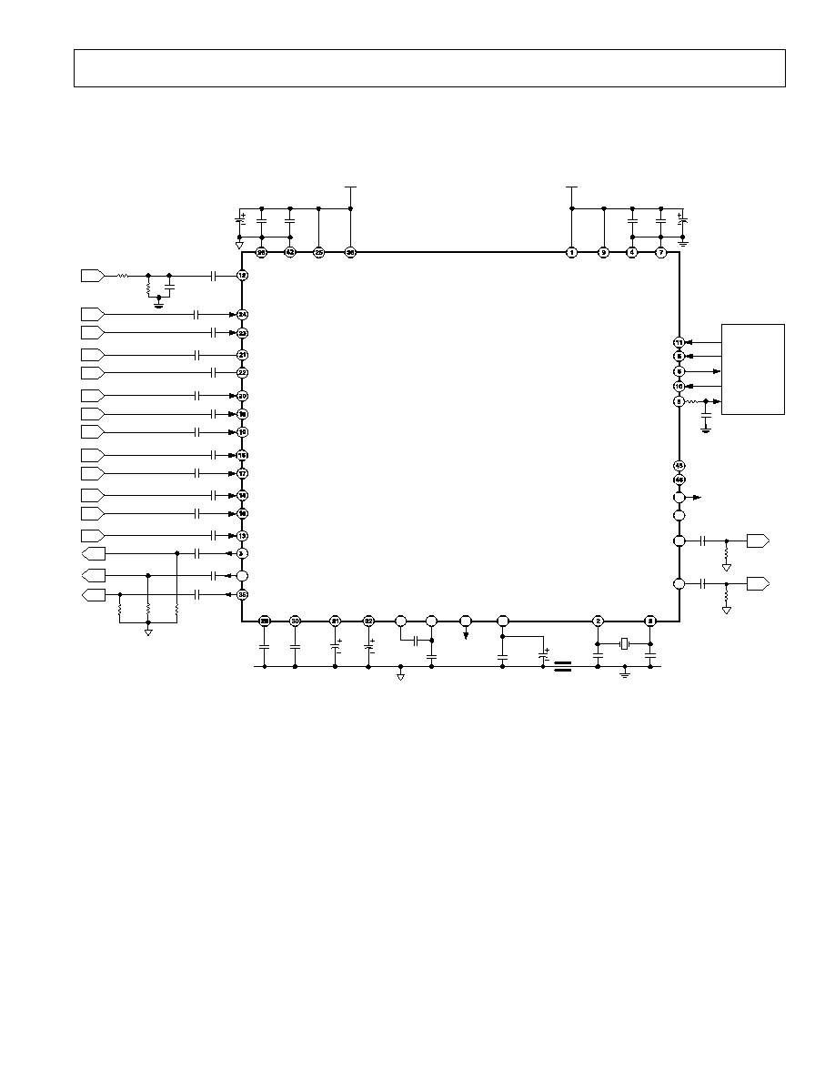
AD1881A
≠21≠
REV. 0
APPLICATIONS CIRCUITS
The AD1881A has been designed to require a minimum amount of external circuitry. The recommended applications circuits are
shown in Figure 9. Reference designs for the AD1881A are available and may be obtained by contacting your local Analog Devices'
sales representative or authorized distributor.
RESET
SDATA_OUT
SDATA_IN
SYNC
BIT_CLK
CS0
CS1
EAPD
MODE
DIGITAL
CONTROLLER
10 F
100nF
+5AV
DD
AV
DD2
AV
SS2
AV
DD1
AV
SS1
DV
SS1
DV
DD1
DV
SS2
DV
DD2
AFILT1
AFILT2
FILT_L
PHONE_IN
MONO_OUT
LINE_OUT_R
LINE_OUT_L
47k
47k
47k
1 F
24.576MHz
22pF
NP0
22pF
NP0
10 F
TANT
100nF
47nF
2.25V
DC
100nF
1 F
270pF
NP0
270pF
NP0
FILT_R CX3D
RX3D V
REFOUT
V
REF
XTL_IN
XTL_OUT
600Z
ANALOG GROUND
DIGITAL GROUND
AD1881A
PC_BEEP
LINE_IN_R
LINE_IN_L
MIC1
MIC2
CD_R
CD_L
CD_GND
VIDEO_L
VIDEO_R
AUX_L
AUX_R
0.33 F
0.33 F
0.33 F
0.33 F
0.33 F
0.33 F
0.33 F
7
36
34
33
27
10k
47
48
1k
100nF
100nF
28
0.33 F
0.33 F
0.33 F
0.33 F
0.33 F
0.33 F
47pF
47
100nF
100nF
100nF
+3.3DV
DD
10 F
39
41
47k
1 F
47k
1 F
LNLVL_OUT_L
LNLVL_OUT_R
1 F
1 F
EAPD
NOTE: FOR OPTIMAL PERFORMANCE USE A REGULATED ANALOG POWER SUPPLY.
Figure 9. Recommended One Codec Application Circuit
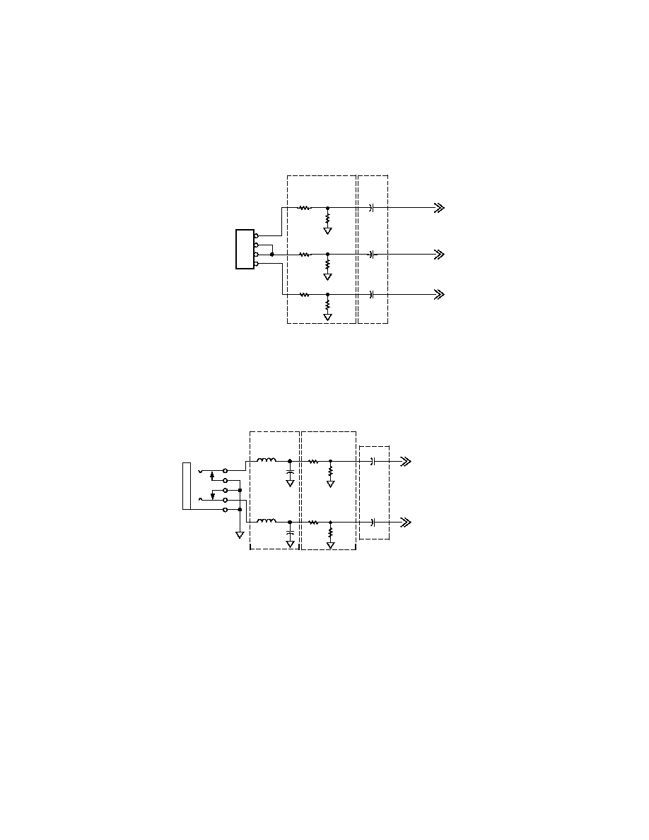
AD1881A
≠22≠
REV. 0
CD-ROM CONNECTIONS
The CD-ROM audio output level should be investigated; typical drives generate 2 V rms output and require a voltage divider for
compatibility with the Codec input (1 V rms range). The recommended circuit is basically a group of divide-by-two voltage dividers
as shown on Figure 10.
The CD_GND_REF pin is used to cancel differential ground noise from the CD-ROM. For optimum noise cancellation, this section
of the divider should have approximately half the impedance of the right and left channel section dividers.
HEADER FOR
CD ROM AUDIO
(LGGR)
1
2
3
4
VOLTAGE
DIVIDER
R1
4.7k
R3
2.7k
4.7k
R5
R2
4.7k
R4
2.7k
R6
4.7k
C1
0.33 F
0.33 F
0.33 F
C2
C3
TO CODEC
CD_L INPUT
TO CODEC
CD_GND_REF
INPUT
TO CODEC
CD_R INPUT
+
+
+
Figure 10. Typical CD-ROM Audio Connections
LINE_IN, AUX AND VIDEO INPUT CONNECTIONS
Most of these audio sources also generate 2 V rms audio level and require a ≠6 dB input voltage divider to be compatible with the
Codec inputs. Figure 11 shows the recommended application circuit. For applications requiring EMC compliance, the EMC compo-
nents should be configured and selected to provide adequate RF immunity and emissions control.
1
2
3
4
R1
4.7k
R2
4.7k
C3
0.33 F
0.33 F
C4
TO CODEC
RIGHT CHANNEL
INPUT
+
+
5
R3
4.7k
R4
4.7k
TO CODEC
LEFT CHANNEL
INPUT
L2 600Z
L1 600Z
C1
470pF
C2
470pF
EMC
COMPONENTS
VOLTAGE
DIVIDER
AC-COUPLING
LINE/AUX/VIDEO
INPUT
J1
Figure 11. LINE_IN, AUX, and Video Input Connections
MICROPHONE CONNECTIONS
The AD1881A contains an internal microphone preamp with 20 dB gain, in most cases a direct microphone connection as shown in
Figure 12 is adequate. If the microphone level is too low, an external preamp can be added as shown in Figure 13. In either case the
microphone bias can be derived from the Codec's internal reference (V
REFOUT
) using a 2.2 k
resistor. For the preamp circuit, the
V
REFOUT
signal can also provide the mid-point bias for the amplifier.
To meet the PC99 1.0A requirements, the MIC signal should be placed on the microphone jack tip and the bias on the ring. This
configuration supports electret microphones with three conductor plugs, as well as dynamic microphones with two conductor plugs
(ring and sleeve shorted together).
Additional filtering may be required to limit the microphone response to the audio band of interest.

AD1881A
≠23≠
REV. 0
1
2
3
4
C3
0.22 F
2.2k
R1
TO CODEC
MIC1 OR MIC2
INPUT
5
FROM CODEC
V
REFOUT
L1 600Z
L2 600Z
C1
470pF
C2
470pF
EMC COMPONENTS
MIC INPUT
J1
AC-COUPLING
Figure 12. Recommended Microphone Input Connections
R2
10k
R3
100k
PREAMP
AD8531
U1
1
2
3
4
C3
0.22 F
2.2k
R1
TO CODEC
MIC1 OR MIC2
INPUT
5
FROM CODEC
V
REFOUT
L1 600Z
L2 600Z
C1
470pF
C2
470pF
EMC COMPONENTS
MIC INPUT
J1
AC-COUPLING
C3
0.22 F
AC-COUPLING
MIC BIAS
+5AV
DD
Figure 13. Microphone with Additional External Preamp (20 dB Gain)
LINE OUTPUT CONNECTIONS
The AD1881A Codec provides stereo LINE_OUT signals at a standard 1 V rms level. These signals must be ac-coupled before they
can be connected to an external load. After the ac-coupling, a minimal resistive load is recommended to keep the capacitors properly
biased and reduce click and pop when plugging stereo equipment into the output jack. The capacitor values should be selected
to provide a desired frequency response, taking into account the nominal impedance of the external load. To meet the PC99
specification for PCs, testing must be performed with a 10 k
load, therefore a 1 µF value is recommended to achieve less than
≠3 dB roll-off at 20 Hz.
FROM CODEC
LINE_OUT_R
L2 600Z
L1 600Z
C1
470pF
C2
470pF
EMC COMPONENTS
STEREO
LINE_OUT JACK
J1
C1
1 F
1 F
C2
+
+
AC-COUPLING
R1
47k
R2
47k
FROM CODEC
LINE_OUT_L
NOTE: IF AN OUTPUT AMP IS USED,
THE AC-COUPLING CAP VALUES WILL
DEPEND ON THE AMP DESIGN.
Figure 14. Recommended LINE_OUT Connections
USING AN EXTERNAL HEADPHONE/POWER AMP
The SSM2250 Power Amplifier is an ideal companion for the AD1881A. The amplifier can provide up to 250 mW output in stereo
mode and up to 1.5 W into a mono speaker connected in a bridge-tied load (BTL) configuration.
The SM2250 has a mode control pin that can be used to switch between the stereo output mode and the mono BTL speaker.
Figure 15 shows a typical PC configuration where the SSM2250 drives a set of stereo headphones or external speakers, as well as an
internal mono speaker. One of the normalizing pins on the stereo jack senses the stereo plug insertion and automatically switches
from driving the internal mono speaker to driving the external stereo load.
To conserve power, the SSM2250 can be shut down by the EAPD pin on the AD1881A, using proper power management software.
This is particularly important for portable applications. In shutdown mode, the SSM2250 consumes only 60
µA.

AD1881A
≠24≠
REV. 0
EAPD/CHAIN_IN
MONO_OUT
LINE_OUT_L
LIN_OUT_R
AD1881A
NC
LEFT IN
SHUTDOWN
SE/BTL
GND
RIGHT IN
NC
NC
LEFT OUT/BLT
VDO
BTL+
BYPASS
RIGHT OUT
NC
U2
SSM2250RU
C4
0.33 F
C7
0.33 F
R4
49.9k
R6
49.9k
NC = NO CONNECT
R2
49.9k
U1
R7
49.9k
C8
0.1 F
C1
1 F
R1
100k
C2
100 F
R3
1k
FB
600Z
C3
470pF
C5
100 F
R5
1k
FB
600Z
C6
470pF
F1
F2
STEREO
HP/SPEAKER
OUTPUT
J1
STEREO
3.5mm JACK
LS1
INTERNAL
MONO
SPEAKER
4
5AV
DD
Figure 15. Using the SSM2250 Amplifier for Stereo and Mono Output
GROUNDING AND LAYOUT
To reduce noise and emissions, Analog Devices recommends a split ground plane as shown in Figure 16. The purpose of splitting the
ground plane is to create a low noise analog area that is somewhat isolated from the digital ground current noise generated by the
system's logic. All the analog circuitry should be placed on the analog ground plane area.
For reference purposes, and to return power supply currents, the analog and digital ground planes must be connected at some point,
ideally a small bridge under or near the Codec should be provided. A 0
resistor or a ferrite bead should also be considered since
these allow some flexibility in optimizing the layout to meet EMC requirements.
PIN 1
ISOLATION
TRENCH
CONNECT SPLIT GROUND
PLANES AT OR NEAR CODEC.
ANALOG
GROUND PLANE
DIGITAL
GROUND PLANE
AD1881A
Figure 16. Recommended Split Ground Plane
ANALOG POWER SUPPLY
To minimize audio noise, the Codec analog power supply (AVDD) should be well decoupled and regulated. In PC systems it is rec-
ommended that the analog supply be derived from the 12 V PC power supply using a localized linear voltage regulator. Preferably,
the analog power supply should be connected to the Codec's analog section using a ferrite bead.

AD1881A
≠25≠
REV. 0
C2
0.1
600Z
12V
L1
F
3
OUT
C1
+
LM78M05CP
IN
GND
5AV
DD
C3
C4
10
U1
2
+
R1
0
10 F
0.1 F
F
Figure 17. Recommended Regulator Circuit for Analog Power Supply
If a power plane layer is being used in the system design, it is recommended that the analog power plane for the Codec also be split
(mirroring the analog ground plane). In this case, the analog power supply ferrite bead should bridge the isolation trench, close to the
Codec location.
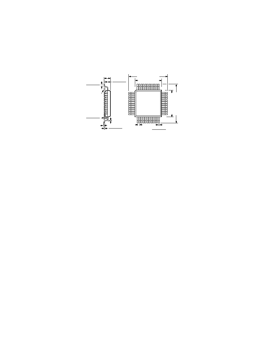
AD1881A
≠26≠
REV. 0
OUTLINE DIMENSIONS
Dimensions shown in inches and (mm).
48-Lead Thin Plastic Quad Flatpack (LQFP)
(ST-48)
0.276 (7.0) BSC
1
12
13
25
24
36
37
48
TOP VIEW
(PINS DOWN)
0.276 (7.0) BSC
0.354 (9.00) BSC
0.011 (0.27)
0.006 (0.17)
0.020 (0.5)
BSC
0.354 (9.00) BSC
SEATING
PLANE
0.063 (1.60) MAX
0∞ MIN
0∞ ≠ 7∞
0.006 (0.15)
0.002 (0.05)
0.030 (0.75)
0.018 (0.45)
0.057 (1.45)
0.053 (1.35)
0.030 (0.75)
0.018 (0.45)
0.007 (0.18)
0.004 (0.09)
C3747≠8≠4/00 (rev. 0) 00752
PRINTED IN U.S.A.