Document Outline
- Specifications
- Pinout
- Package Drawings
- Ordering Guide
- Features
- Absolute Maximum Ratings
- Functional Block Diagram
- Pin Function Description
- ANALOG INPUT
- MASTER VOLUME
- PROGRAMMABLE GAIN AMPLIFIERÑADC
- ANALOG MIXERÑINPUT GAIN / AMPLIFIERS / ATTENUATORS
- DIGITAL DECIMATION AND INTERPOLATION FILTERS*
- ANALOG-TO-DIGITAL CONVERTERS
- DIGITAL-TO-ANALOG CONVERTERS
- ANALOG OUTPUT
- STATIC DIGITAL SPECIFICATIONS
- POWER SUPPLY
- CLOCK SPECIFICATIONS*
- POWER-DOWN STATES
- TIMING PARAMETERS (GUARANTEED OVER OPERATING TEMPERATURE RANGE)
- ABSOLUTE MAXIMUM RATINGS*
- ENVIRONMENTAL CONDITIONS
- CAUTION
- Digital I/O
- CHIP SELECTS
- JACK SENSE/GENERAL-PURPOSE DIGITAL OUTPUT
- Analog I/O
- Filter/Reference
- Power and Ground Signals
- No Connects
- Indexed Control Registers
- Reset (Index 00h)
- Master Volume Registers (Index 02h)
- Headphones Volume Registers (Index 04h)
- Master Volume Mono (Index 06h)
- PC Beep Register (Index 0Ah)
- Phone Volume (Index 0Ch)
- Mic Volume (Index 0Eh)
- Line In Volume (Index 10h)
- CD Volume (Index 12h)
- Video Volume (Index 14h)
- AUX Volume (Index 16h)
- PCM Out Volume (Index 18h)
- Record Select Control Register (Index 1Ah)
- Record Gain (Index 1Ch)
- General-Purpose Register (Index 20h)
- 3D Control Register (Index 22h)
- Subsection Ready Register (Index 26h)
- Extended Audio ID Register (Index 28h)
- Extended Audio Status and Control Register (Index 2Ah)
- PCM DAC Rate Register (Index 2Ch)
- PCM ADC Rate Register (Index 32h)
- SPDIF Control Register (Index 3Ah)
- Jack Sense/SPDIF Register (Index 72h)
- Serial Configuration (Index 74h)
- Miscellaneous Control Bits (Index 76h)
- Sample Rate 0 (Index 78h)
- Sample Rate 1 (Index 7Ah)
- Vendor ID1 Register (Index 7Ch)
- Vendor ID2 Register (Index 7Eh)
- SPDIF TRANSMITTER OUTPUT CONNECTION
- JACK SENSE OPERATION
- CONNECTING THE JACK SENSE TO THE OUTPUT JACKS
- LINE OUT JACK
- APPLICATION CIRCUITS CD-ROM CONNECTIONS
- LINE_IN, AUX, AND VIDEO INPUT CONNECTIONS
- MICROPHONE CONNECTIONS
- LINE OUTPUT CONNECTIONS
- PC BEEP INPUT CONNECTIONS
- DIAGRAMS
- Cold Reset
- Warm Reset
- Clock Timing
- Data Setup and Hold
- Signal Rise and Fall Time
- AC Link Low Power Mode Timing
- ATE Test Mode
- Block Diagram Register Map
- Recommended Power Connections, Decoupling and Support Components
- SPDIF Output Connection Using Optical LINK
- SPDIF Output Connection Using Electrical Link
- Jack Sense Connection to HP_OUT Jack, Using Isolated Switch
- Jack Sense Connection to HP_OUT Jack, Using Nonisolated Switch
- Typical CD-ROM Audio Connections
- LINE_IN, AUX and VIDEO Input Connections
- Recommended Microphone Input Connections
- Microphone with Additional External Preamp (20 dB Gain)
- Recommended LINE_OUT Connections
- Recommended PC_BEEP Connections
REV. 0
Information furnished by Analog Devices is believed to be accurate and
reliable. However, no responsibility is assumed by Analog Devices for its
use, nor for any infringements of patents or other rights of third parties that
may result from its use. No license is granted by implication or otherwise
under any patent or patent rights of Analog Devices.
a
AD1886A
One Technology Way, P.O. Box 9106, Norwood, MA 02062-9106, U.S.A.
Tel: 781/329-4700
www.analog.com
Fax: 781/326-8703
© Analog Devices, Inc., 2001
AC'97 SoundMAX
Æ
Codec
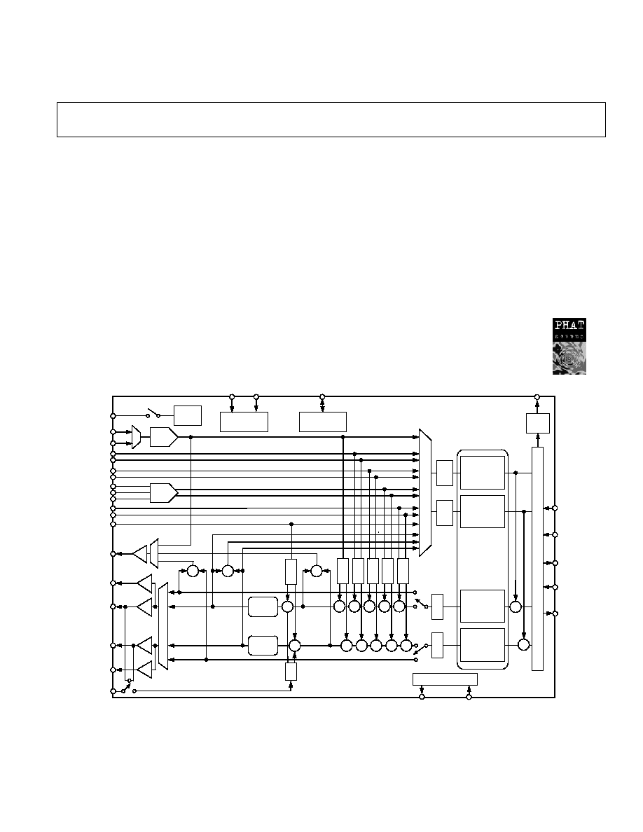
FUNCTIONAL BLOCK DIAGRAM
G
A
M
G
A
M
G
A
M
SYNC
BIT_CLK
G
A
M
A
M
AD1886A
MIC1
MIC2
AUX
CD
VIDEO
LINE_OUT_L
MONO_OUT
LINE
PHONE_IN
LINE_OUT_R
SELECT
O
R
G
A
M
OSCILLATOR
XTAL_OUT
XTAL_IN
RESET
SDATA_IN
JS
SDATA_OUT
G
A
M
G
A
M
16-BIT
- D/A
CONVERTER
16-BIT
- D/A
CONVERTER
SPDIF
MV
HP_OUT_R
HP_OUT_L
0dB/
20dB
PGA
PGA
16-BIT
- A/D
CONVERTER
16-BIT
- A/D
CONVERTER
SAMPLE
RATE
GENERATORS
A
C
LINK
PHAT
STEREO
G = GAIN
A = ATTENUATE
M = MUTE
PHAT
STEREO
MV
MV
MV
MV
CHIP SELECT
VREF
ID1
ID0
SPDIF
OUT
V
REFOUT
G
A
M
PC_BEEP
JACK SENSE
AC'97 2.1 FEATURES
Variable Sample Rate Audio
Multiple Codec Configuration Options
External Audio Power-Down Control
AC'97 FEATURES
AC'97 2.2 Compliant
Greater than 90 dB Dynamic Range
Stereo Headphone Amplifier
Multibit - Converter Architecture for Improved S/N
Ratio Greater than 90 dB
16-Bit Stereo Full-Duplex Codec
Four Analog Line-Level Stereo Inputs for:
LINE-IN, CD, VIDEO, and AUX
Two Analog Line-Level Mono Inputs for Speakerphone
and PC BEEP
Mono MIC Input w/Built-In 20 dB Preamp, Switchable
from Two External Sources
High-Quality CD Input with Ground Sense
Stereo Line Level Outputs
Mono Output for Speakerphone or Internal Speaker
Power Management Support
48-Terminal LQFP Package
ENHANCED FEATURES
20-Bit SPDIF Output w/32 kHz, 44.1 kHz, and 48 kHz
Symbol Rates
Full Duplex Variable Sample Rates from 7040 Hz to
48 kHz with 1 Hz Resolution
Jack Sense Pins Provide Automatic Output Switching
Software-Enabled V
REFOUT
Output for Microphones and
External Power Amp
Split Power Supplies (3.3 V Digital/5 V Analog)
Mobile Low-Power Mixer Mode
Extended 6-Bit Master Volume Control
Extended 6-Bit Headphone Volume Control
Digital Audio Mixer Mode
PhatTM Stereo 3D Stereo Enhancement
SoundMAX is a registered trademark and Phat is a trademark of Analog Devices, Inc.

REV. 0
≠2≠
AD1886A≠SPECIFICATIONS
ANALOG INPUT
Parameter
Min
Typ
Max
Unit
Input Voltage (RMS Values Assume Sine Wave Input)
LINE_IN, AUX, CD, VIDEO, PHONE_IN, PC_BEEP
1
V rms
2.83
V p-p
MIC1 or MIC2 with +20 dB Gain (M20 = 1)
0.1
V rms
0.283
V p-p
MIC1 or MIC2 with 0 dB Gain (M20 = 0)
1
V rms
2.83
V p-p
Input Impedance
*
20
k
Input Capacitance
*
5
7.5
pF
MASTER VOLUME
Parameter
Min
Typ
Max
Unit
Step Size (0 dB to ≠94.5 dB); LINE_OUT_L, LINE_OUT_R
1.5
dB
Output Attenuation Range Span
*
≠94.5
dB
Step Size (0 dB to ≠46.5 dB); MONO_OUT
1.5
dB
Output Attenuation Range Span
*
≠46.5
dB
Step Size (+6 dB to ≠88.5 dB); HP_OUT_R, HP_OUT_L
1.5
dB
Output Attenuation Range Span
*
≠94.5
dB
Mute Attenuation of 0 dB Fundamental
*
80
dB
PROGRAMMABLE GAIN AMPLIFIER--ADC
Parameter
Min
Typ
Max
Unit
Step Size (0 dB to 22.5 dB)
1.5
dB
PGA Gain Range Span
22.5
dB
ANALOG MIXER--INPUT GAIN / AMPLIFIERS / ATTENUATORS
Parameter
Min
Typ
Max
Unit
Signal-to-Noise Ratio (SNR)
CD to LINE_OUT
90
dB
Other to LINE_OUT
90
dB
Step Size (+12 dB to ≠34.5 dB): (All Steps Tested)
MIC, LINE_IN, AUX, CD, VIDEO, PHONE_IN, DAC
1.5
dB
Input Gain/Attenuation Range:
MIC, LINE, AUX, CD, VIDEO, PHONE_IN, DAC
≠46.5
dB
Step Size (0 dB to ≠45 dB): (All Steps Tested)
PC_BEEP
3.0
dB
Input Gain/Attenuation Range: PC_BEEP
≠45
dB
*Guaranteed but not tested.
STANDARD TEST CONDITIONS UNLESS OTHERWISE NOTED
Temperature
25
∞C
Digital Supply (V
DD
)
3.3 V
Analog Supply (V
CC
)
5.0 V
Sample Rate (f
S
)
48 kHz
Input Signal
1008 Hz
Analog Output Pass Band
20 Hz to 20 kHz
V
IH
2.0 V
V
IL
0.8 V
V
IH
(CS0, CS1, CHAIN_IN)
4.0 V
V
IL
1.0 V
DAC Test Conditions
Calibrated
≠3 dB Attenuation Relative to Full Scale
Input 0 dB
10 k
Output Load (LINE_OUT)
32
Output Load (HP_OUT)
ADC Test Conditions
Calibrated
0 dB Gain
Input ≠3.0 dB Relative to Full Scale

REV. 0
≠3≠
AD1886A
DIGITAL DECIMATION AND INTERPOLATION FILTERS
*
Parameter
Min
Typ
Max
Unit
Pass Band
0
0.4
◊ f
S
Hz
Pass-Band Ripple
±0.09
dB
Transition Band
0.4
◊ f
S
0.6
◊ f
S
Hz
Stop Band
0.6
◊ f
S
Hz
Stop-Band Rejection
≠74
dB
Group Delay
12/f
S
sec
Group Delay Variation over Pass Band
0.0
µs
ANALOG-TO-DIGITAL CONVERTERS
Parameter
Min
Typ
Max
Unit
Resolution
16
Bits
Total Harmonic Distortion (THD)
≠84
dB
Dynamic Range (≠60 dB input THD + N Referenced to Full Scale, A-Weighted)
84
87
dB
Signal-to-Intermodulation Distortion
* (CCIF Method)
85
dB
ADC Crosstalk
*
Line Inputs (Input L, Ground R, Read R; Input R, Ground L, Read L)
≠100
≠90
dB
LINE_IN to Other
≠90
≠85
dB
Gain Error (Full-Scale Span Relative to Nominal Input Voltage)
±10
%
Interchannel Gain Mismatch (Difference of Gain Errors)
±0.5
dB
ADC Offset Error
±5
mV
DIGITAL-TO-ANALOG CONVERTERS
Parameter
Min
Typ
Max
Unit
Resolution
16
Bits
Total Harmonic Distortion (THD) LINE_OUT
≠85
dB
Total Harmonic Distortion (THD) HP_OUT
≠75
dB
Dynamic Range (≠60 dB Input THD + N Referenced to Full Scale, A-Weighted)
85
90
dB
Signal-to-Intermodulation Distortion
* (CCIF Method)
≠100
dB
Gain Error (Full-Scale Span Relative to Nominal Input Voltage)
±10
%
Interchannel Gain Mismatch (Difference of Gain Errors)
±0.7
dB
DAC Crosstalk
* (Input L, Zero R, Measure R_OUT; Input R, Zero L,
≠80
dB
Measure L_OUT)
Total Audible Out-of-Band Energy (Measured from 0.6
◊ f
S
to 20 kHz)
*
≠40
dB
ANALOG OUTPUT
Parameter
Min
Typ
Max
Unit
Full-Scale Output Voltage; LINE_OUT
1
V rms
2.83
V p-p
Output Impedance
*
800
External Load Impedance
*
10
k
Output Capacitance
*
15
pF
External Load Capacitance
100
pF
Full-Scale Output Voltage; HP_OUT (0 dB Gain)
1
V rms
Output Capacitance
*
100
pF
External Load Impedance
*
32
V
REF
2.05
2.25
2.45
V
V
REF_OUT
2.25
V
V
REF _OUT
Current Drive
5
mA
Mute Click (Muted Output Minus Unmuted Midscale DAC Output)
±5
mV
*Guaranteed but not tested.

REV. 0
≠4≠
AD1886A≠SPECIFICATIONS
STATIC DIGITAL SPECIFICATIONS
Parameter
Min
Typ
Max
Unit
High-Level Input Voltage (V
IH
): Digital Inputs
0.65
◊ DV
DD
V
Low-Level Input Voltage (V
IL
)
0.35
◊ DV
DD
V
High-Level Output Voltage (V
OH
), I
OH
= 2 mA
0.9
◊ DV
DD
V
Low-Level Output Voltage (V
OL
), I
OL
= 2 mA
0.1
◊ DV
DD
V
Input Leakage Current
≠10
+10
µA
Output Leakage Current
≠10
+10
µA
POWER SUPPLY
Parameter
Min
Typ
Max
Unit
Power Supply Range--Analog (AV
DD
)
4.75
5.0
5.25
V
Power Supply Range--Digital (DV
DD
)
3.0
3.3
3.6
V
Power Dissipation--5 V/3.3 V
306
mW
Analog Supply Current--5 V (AV
DD
)
48
mA
Digital Supply Current--3.3 V (DV
DD
)
20
mA
Power Supply Rejection (100 mV p-p Signal @ 1 kHz)
*
40
dB
(At Both Analog and Digital Supply Pins, Both ADCs and DACs)
CLOCK SPECIFICATIONS
*
Parameter
Min
Typ
Max
Unit
Input Clock Frequency
24.576
MHz
Recommended Clock Duty Cycle
40
50
60
%
POWER-DOWN STATES
Parameter
Set Bits
DV
DD
Typ
AV
DD
Typ
Unit
ADC
PR0
17.5
41.6
mA
DAC
PR1
17.0
38.3
mA
ADC + DAC
PR1, PR0
4.1
31.9
mA
ADC + DAC + Mixer (Analog CD On)
LPMIX, PR1, PR0
4.1
22.4
mA
Mixer
PR2
20
17.5
mA
ADC + Mixer
PR2, PR0
17.6
11.2
mA
DAC + Mixer
PR2, PR1
17
8.4
mA
ADC + DAC + Mixer
PR2, PR1, PR0
4.1
2.2
mA
Analog CD Only (AC-Link On)
LPMIX, PR5, PR1, PR0
4.1
22.4
mA
Analog CD Only (AC-Link Off)
LPMIX, PR1, PR0, PR4, PR5
0
22.4
mA
Standby
PR5, PR4, PR3, PR2, PR1, PR0
0
0
mA
Headphone Standby
PR6
20
38.8
mA
*Guaranteed but not tested.
Specifications subject to change without notice.

REV. 0
AD1886A
≠5≠
TIMING PARAMETERS (GUARANTEED OVER OPERATING TEMPERATURE RANGE)
Parameter
Symbol
Min
Typ
Max
Unit
RESET Active Low Pulsewidth
t
RST_LOW
1.0
µs
RESET Inactive to BIT_CLK Startup Delay
t
RST2CLK
162.8
ns
SYNC Active High Pulsewidth
t
SYNC_HIGH
1.3
ms
SYNC Low Pulsewidth
t
SYNC_LOW
19.5
µs
SYNC Inactive to BIT_CLK Startup Delay
t
SYNC2CLK
162.8
ns
BIT_CLK Frequency
12.288
MHz
BIT_CLK Period
t
CLK_PERIOD
81.4
ns
BIT_CLK Output Jitter
*
750
ps
BIT_CLK High Pulsewidth
t
CLK_HIGH
32.56
42
48.84
ns
BIT_CLK Low Pulsewidth
t
CLK_LOW
32.56
38
48.84
ns
SYNC Frequency
48.0
kHz
SYNC Period
t
SYNC_PERIOD
20.8
µs
Setup to Falling Edge of BIT_CLK
t
SETUP
5
2.5
ns
Hold from Falling Edge of BIT_CLK
t
HOLD
5
ns
BIT_CLK Rise Time
t
RISECLK
2
4
6
ns
BIT_CLK Fall Time
t
FALLCLK
2
4
6
ns
SYNC Rise Time
t
RISESYNC
2
4
6
ns
SYNC Fall Time
t
FALLSYNC
2
4
6
ns
SDATA_IN Rise Time
t
RISEDIN
2
4
6
ns
SDATA_IN Fall Time
t
FALLDIN
2
4
6
ns
SDATA_OUT Rise Time
t
RISEDOUT
2
4
6
ns
SDATA_OUT Fall Time
t
FALLDOUT
2
4
6
ns
End of Slot 2 to BIT_CLK, SDATA_IN Low
t
S2_PDOWN
0
1.0
µs
Setup to Trailing Edge of RESET (Applies to SYNC, SDATA_OUT)
t
SETUP2RST
15
ns
Rising Edge of RESET to HI-Z Delay
t
OFF
25
ns
Propagation Delay
15
ns
RESET Rise Time
50
ns
Output Valid Delay from Rising Edge of BIT_CLK to SDI Valid
15
ns
*Guaranteed but not tested.
Specifications subject to change without notice.

REV. 0
AD1886A
≠6≠
RESET
BIT_CLK
t
RST2CLK
t
RST_LOW
Figure 1. Cold Reset
SYNC
BIT_CLK
t
SYNC_HIGH
t
RST2CLK
Figure 2. Warm Reset
t
CLK_HIGH
BIT_CLK
t
CLK_LOW
SYNC
t
SYNC_HIGH
t
SYNC_LOW
t
SYNC_PERIOD
t
CLK_PERIOD
Figure 3. Clock Timing
BIT_CLK
SYNC
t
HOLD
SDATA_OUT
t
SETUP
Figure 4. Data Setup and Hold
BIT_CLK
SYNC
SDATA_IN
t
RISECLK
t
RISESYNC
t
RISEDIN
t
RISEDOUT
t
FALLCLK
t
FALLSYNC
t
FALLDIN
t
FALLDOUT
SDATA_OUT
Figure 5. Signal Rise and Fall Time
BIT_CLK
SDATA_OUT
SYNC
SDATA_IN
SLOT 1
SLOT 2
WRITE
TO 0x26
DATA
PR4
DON'T
CARE
t
S2_PDOWN
NOTE: BIT_CLK NOT TO SCALE
Figure 6. AC Link Low Power Mode Timing
RESET
SDATA_OUT
HI-Z
t
SETUP2RST
t
OFF
SDATA_IN, BIT_CLK
Figure 7. ATE Test Mode

REV. 0
AD1886A
≠7≠
CAUTION
ESD (electrostatic discharge) sensitive device. Electrostatic charges as high as 4000 V readily
accumulate on the human body and test equipment and can discharge without detection. Although
the AD1886A features proprietary ESD protection circuitry, permanent damage may occur on
devices subjected to high-energy electrostatic discharges. Therefore, proper ESD precautions are
recommended to avoid performance degradation or loss of functionality.
ABSOLUTE MAXIMUM RATINGS
*
Parameter
Min
Max
Unit
Power Supplies
Digital (DV
DD
)
≠0.3
+3.6
V
Analog (AV
CC
)
≠0.3
+6.0
V
Input Current (Except Supply Pins)
±10.0
mA
Analog Input Voltage (Signal Pins)
≠0.3
AV
DD
+ 0.3
V
Digital Input Voltage (Signal Pins)
≠0.3
DV
DD
+ 0.3
V
Ambient Temperature (Operating)
0
70
∞C
Storage Temperature
≠65
+150
∞C
*Stresses greater than those listed under Absolute Maximum Ratings may cause
permanent damage to the device. This is a stress rating only; functional operation
of the device at these or any other conditions above those indicated in the
operational section of this specification is not implied. Exposure to absolute
maximum rating conditions for extended periods may affect device reliability.
ORDERING GUIDE
Temperature
Package
Package
Model
Range
Description
Option
*
AD1886AJST 0
∞C to 70∞C
48-Lead LQFP
ST-48
*ST = Thin Quad Flatpack.
WARNING!
ESD SENSITIVE DEVICE
ENVIRONMENTAL CONDITIONS
Ambient Temperature Rating
T
AMB
= T
CASE
≠ (P
D
◊
CA
)
T
CASE
= Case Temperature in
∞C
P
D
= Power Dissipation in W
CA
= Thermal Resistance (Case-to-Ambient)
JA
= Thermal Resistance (Junction-to-Ambient)
JC
= Thermal Resistance (Junction-to-Case)
Package
JA
JC
CA
LQFP
76.2
∞C/W
17
∞C/W
59.2
∞C/W

REV. 0
AD1886A
≠8≠
PIN CONFIGURATION
36
35
34
33
32
31
30
29
28
27
26
25
13 14 15 16 17 18 19 20 21 22 23 24
1
2
3
4
5
6
7
8
9
10
11
12
48 47 46 45 44
39 38 37
43 42 41 40
PIN 1
IDENTIFIER
TOP VIEW
(Not to Scale)
LINE_OUT_R
LINE_OUT_L
CX3D
RX3D
FILT_L
FILT_R
AFILT2
DV
DD1
XTL_IN
XTL_OUT
DV
SS1
SDATA_OUT
BIT_CLK
DV
SS2
SDATA_IN
DV
DD2
SYNC
RESET
AFILT1
V
REFOUT
V
REF
AV
SS1
AD1886A
PC_BEEP
AV
DD1
SPDIF
JS
ID1
ID0
AV
SS3
AV
DD3
NC
HP_OUT_R
AV
SS2
HP_OUT_L
AV
DD2
PHONE_IN
AU
X
_
L
AU
X
_
R
VIDEO_L
VIDEO_R
CD_L
CD_GND_REF
CD_R
MIC1
MIC2
LINE_IN_L
LINE_IN_R
MONO_OUT
NC = NO CONNECT
PIN FUNCTION DESCRIPTIONS
Digital I/O
Pin Name
LQFP
I/O
Description
XTL_IN
2
I
Crystal (or Clock) Input, 24.576 MHz.
XTL_OUT
3
O
Crystal Output
SDATA_OUT
5
I
AC-Link Serial Data Output, AD1886A Input Stream.
BIT_CLK
6
O/I
AC-Link Bit Clock. 12.288 MHz Serial Data Clock. Daisy-Chain Output Clock.
SDATA_IN
8
O
AC-Link Serial Data Input. AD1886A Output Stream.
SYNC
10
I
AC-Link Frame Sync
RESET
11
I
AC-Link Reset. AD1886A Master H/W Reset.
SPDIF
48
O
SPDIF Output
CHIP SELECTS
Pin Name
LQFP
Type
Description
ID0
45
I
Chip Select Input 0 (Active Low)
ID1
46
I
Chip Select Input 1 (Active Low)
JACK SENSE/GENERAL-PURPOSE DIGITAL OUTPUT
The JS pin can be used to sense the presence of an audio plug in the output jacks and automatically mute the MONO and/or
LINE_OUT audio outputs. Alternatively, the JS can be programmed as a general-purpose digital output pin.
Pin Name
LQFP
Type
Description
JS
47
I/O
JACK SENSE Input, or GPIO.

REV. 0
AD1886A
≠9≠
Analog I/O
These signals connect the AD1886A component to analog sources and sinks, including microphones and speakers.
Pin Name
LQFP
I/O
Description
PC_BEEP
12
I
PC Beep. PC Speaker beep passthrough.
PHONE
13
I
Phone. From telephony subsystem speakerphone or handset.
AUX_L
14
I
Auxiliary Input Left Channel
AUX_R
15
I
Auxiliary Input Right Channel
VIDEO_L
16
I
Video Audio Left Channel
VIDEO_R
17
I
Video Audio Right Channel
CD_L
18
I
CD Audio Left Channel
CD_GND_REF
19
I
CD Audio Analog Ground Reference for CD Input
CD_ R
20
I
CD Audio Right Channel
MIC1
21
I
Microphone 1. Desktop microphone input.
MIC2
22
I
Microphone 2. Second microphone input.
LINE_IN_L
23
I
Line In, Left Channel.
LINE_IN_R
24
I
Line In, Right Channel.
LINE_OUT_L
35
O
Line Out, Left Channel.
LINE_OUT_R
36
O
Line Out, Right Channel.
MONO_OUT
37
O
Monaural Output to Telephony Subsystem Speakerphone
HP_OUT_L
39
O
Headphones Out, Left Channel.
HP_OUT_R
41
O
Headphones Out, Right Channel.
Filter/Reference
These signals are connected to resistors, capacitors, or specific voltages.
Pin Name
LQFP
I/O
Description
V
REF
27
O
Voltage Reference Filter
V
REFOUT
28
O
Voltage Reference Output 5 mA Drive. (Intended for Mic Bias.)
AFILT1
29
O
Antialiasing Filter Capacitor--ADC Right Channel.
AFLIT2
30
O
Antialiasing Filter Capacitor--ADC Left Channel.
FILT_R
31
O
AC-Coupling Filter Capacitor--ADC Right Channel.
FILT_L
32
O
AC-Coupling Filter Capacitor--ADC Left Channel.
RX3D
33
O
3D Phat Stereo Enhancement--Resistor.
CX3D
34
I
3D Phat Stereo Enhancement--Capacitor.
Power and Ground Signals
Pin Name
LQFP
Type
Description
DV
DD
1
1
I
Digital V
DD
3.3 V
DV
SS
1
4
I
Digital GND
DV
SS
2
7
I
Digital GND
DV
DD
2
9
I
Digital V
DD
3.3 V
AV
DD
1
2 5
I
Analog V
DD
5.0 V
AV
SS
1
2 6
I
Analog GND
AV
DD
2
3 8
I
Analog V
DD
5.0 V
AV
SS
2
4 0
I
Analog GND
AV
DD
3
4 3
I
Analog V
DD
5.0 V
AV
SS
3
4 4
I
Analog GND
No Connects
Pin Name
LQFP
Type
Description
NC
42
No Connect

REV. 0
AD1886A
≠10≠
RESET
SYNC
BIT_CLK
SDATA_OUT
SDATA_IN
M 0x02
MM
MMM
M 0x06
S 0x20
MIX
M 0x02
MM
A 0x02
LMV
MS
0
1
S 0x20
OSCILLATORS
M 0x0C
PHM
GA 0x0C
PHV
A 0x0A
PCV
M 0x0A
PCM
GM 0x1C
RIM
IM
GM 0x1C
LIM
IM
LS/RS (0)
LS (4)
RS (4)
LS (3)
RS (3)
LS (1)
RS (1)
LS/RS (6)
RS (5)
LS (2)
RS (2)
S 0x1A
S
E
L
E
C
T
O
R
LS/RS (7)
LS (5)
3D 0x20
SWITCH
M 0x14
VM
M 0x12
CM
M 0x16
AM
M 0x10
LM
M 0x0E
MCM
3D 0x22
POP3D
GM 0x1C
LIV
IM
GA 0x14
LVV
RVV
GA 0x16
LCV
RCV
GA 0x12
LAV
RAV
GA 0x10
LLV
RLA
GA 0x0E
MCV
GAM 0
x18
LOV
OM
ROV
OM
A
C
LINK
GM 0x1C
RIV
IM
16-BIT
- A/D
16-BIT
- A/D
16-BIT
- D/A
16-BIT
- D/A
3D 0x22
POP3D
0
1
A 0x02
RMV
A 0x06
MMV
MONO_OUT
HP_OUT_L
LINE_OUT_R
PC_BEEP
MIC1
MIC2
AUX
CD
VIDEO
0dB/20dB
M20 0x0E
XTL_OUT
XTL_IN
PHONE_IN
LINE_IN
AD1886A
0x3A
0x2A
0x28
0x72
SPDIF
JACK SENSE
0x72
SPDIF
JS
GAM 0
x18
D
A
M
0x04
HPM
0x04
LHV
LINE_OUT_L
HP_OUT_R
0x04
HPM
0x04
RHV
Figure 8. Block Diagram Register Map

REV. 0
AD1886A
≠11≠
Indexed Control Registers
Reg
Num
Name
D15
D14
D13
D12
D11
D10
D9
D8
D7
D6
D5
D4
D3
D2
D1
D0
Default
00h
Reset
X
SE4
SE3
SE2
SE1
SE0
ID9
ID8
ID7
ID6
ID5
ID4
ID3
ID2
ID1
ID0
0410h
02h
Master Volume
MM
X
LMV5
LMV4
LMV3
LMV2
LMV1
LMV0
X
X
RMV5 RMV4
RMV3
RMV2
RMV1 RMV0
8000h
04h
Headphones Volume
HPM
X
LHV5
LHV4
LHV3
LHV2
LHV1
LHV0
X
X
RHV5
RHV4
RHV3
RHV2
RHV1 RHV0
8000h
06h
Master Volume Mono
MMM
X
X
X
X
X
X
X
X
X
X
MMV4
MMV3
MMV2
MMV1 MMV0
8000h
08h
Reserved
X
X
X
X
X
X
X
X
X
X
X
X
X
X
X
X
X
0Ah
PC Beep Volume
PCM
X
X
X
X
X
X
X
X
X
X
PCV3
PCV2
PCV1
PCV0
X
8000h
0Ch
Phone-In Volume
PHM
X
X
X
X
X
X
X
X
X
X
PHV4
PHV3
PHV2
PHV1
PHV0
8008h
0Eh
Mic Volume
MCM
X
X
X
X
X
X
X
X
M20
X
MCV4
MCV3
MCV2
MCV1 MCV0
8008h
10h
Line-In Volume
LM
X
X
LLV4
LLV3
LLV2
LLV1
LLV0
X
X
X
RLV4
RLV3
RLV2
RLV1
RLV0
8808h
12h
CD Volume
CVM
X
X
LCV4
LCV3
LCV2
LCV1
LCV0
X
X
X
RCV4
RCV3
RCV2
RCV1
RCV0
8808h
14h
Video Volume
VM
X
X
LVV4
LVV3
LVV2
LVV1
LVV0
X
X
X
RVV4
RVV3
RVV2
RVV1
RVV0
8808h
16h
Aux Volume
AM
X
X
LAV4
LAV3
LAV2
LAV1
LAV0
X
X
X
RAV4
RAV3
RAV2
RAV1
RAV0
8808h
18h
PCM Out Vol
OM
X
X
LOV4
LOV3
LOV2
LOV1
LOV0
X
X
X
ROV4
ROV3
ROV2
ROV1
ROV0
8808h
1Ah
Record Select
X
X
X
X
X
LS2
LS1
LS0
X
X
X
X
X
RS2
RS1
RS0
0000h
1Ch
Record Gain
IM
X
X
X
LIM3
LIM2
LIM1
LIM0
X
X
X
X
RIM3
RIM2
RIM1
RIM0
8000h
20h
General-Purpose
POP
X
3D
X
X
X
MIX
MS
LPBK X
X
X
X
X
X
X
0000h
22h
3D Control
X
X
X
X
X
X
X
X
X
X
X
X
DP3
DP2
DP1
DP0
0000h
26h
Power-Down Ctrl/Stat
X
X
PR5
PR4
PR3
PR2
PR1
PR0
X
X
X
X
REF
ANL
DAC
ADC
000Xh
28h
Ext'd Audio ID
ID1
ID0
X
X
X
X
X
X
X
X
X
X
X
SPDF
X
VRA
0005h
2Ah
Ext'd Audio Stat/Ctrl
X
X
X
X
X
SPCV
X
X
X
X
SPSA1 SPSA0
X
SPDIF
X
VRA
0000h
2Ch/
PCM DAC Rate (SR1) SR15
SR14
SR13
SR12
SR11
SR10
SR9
SR8
SR7
SR6
SR5
SR4
SR3
SR2
SR1
SR0
BB80h
(7Ah)
*
32h/
PCM ADC Rate (SR0) SR15
SR14
SR13
SR12
SR11
SR10
SR9
SR8
SR7
SR6
SR5
SR4
SR3
SR2
SR1
SR0
BB80h
(78h)
*
3Ah
SPDIF Control
V
X
SPSR1
SPSR0
L
CC6
CC5
CC4
CC3
CC2
CC1
CC0
PRE
COPY
AUD
PRO
0000h
72h
Jack Sense/SPDIF
SPMIX
JSOD
SPRZ
JSPD
X
JSOE
JSLM
JSD
X
JSC
JSMM
JSM
VWI
JS1
JS0
JSI
0000h
74h
Serial Configuration
SLOT16
REGM2 REGM1 REGM0 DRQEN X
X
X
X
X
X
X
X
X
X
X
7000h
76h
Misc Control Bits
DACZ
LPMIX
X
DAM
DMS
DLSR
X
ALSR
MOD SRX1
SRX8
X
X
DRSR
X
ARSR
0404h
EN
0D7
D7
7Ch
Vendor ID1
F7
F6
F5
F4
F3
F2
F1
F0
S7
S6
S5
S4
S3
S2
S1
S0
4144h
7Eh
Vendor ID2
T7
T6
T5
T4
T3
T2
T1
T0
REV7 REV6
REV5
REV4
REV3
REV2
REV1
REV0
5363h
NOTES
All registers not shown and bits containing an X are assumed to be reserved.
Odd register addresses are aliased to the next lower even address.
Reserved registers should not be written.
Zeros should be written to reserved bits.
*Indicates Aliased register for AD1819, AD1819A backward compatibility

REV. 0
AD1886A
≠12≠
Reset (Index 00h)
g
e
R g
e
R g
e
R g
e
R g
e
R
m
u
N m
u
N m
u
N m
u
N m
u
N
e
m
a
N
e
m
a
N
e
m
a
N
e
m
a
N
e
m
a
N
5
1
D 5
1
D 5
1
D 5
1
D 5
1
D
4
1
D 4
1
D 4
1
D 4
1
D 4
1
D
3
1
D 3
1
D 3
1
D 3
1
D 3
1
D
2
1
D 2
1
D 2
1
D 2
1
D 2
1
D
1
1
D 1
1
D 1
1
D 1
1
D 1
1
D
0
1
D 0
1
D 0
1
D 0
1
D 0
1
D
9
D9
D9
D9
D9
D
8
D8
D8
D8
D8
D
7
D7
D7
D7
D7
D
6
D6
D6
D6
D6
D
5
D5
D5
D5
D5
D
4
D4
D4
D4
D4
D
3
D3
D3
D3
D3
D
2
D2
D2
D2
D2
D
1
D1
D1
D1
D1
D
0
D0
D0
D0
D0
D
t
l
u
a
f
e
D
t
l
u
a
f
e
D
t
l
u
a
f
e
D
t
l
u
a
f
e
D
t
l
u
a
f
e
D
h
0
0 h
0
0 h
0
0 h
0
0 h
0
0
t
e
s
e
R
t
e
s
e
R
t
e
s
e
R
t
e
s
e
R
t
e
s
e
R
X
X
X
X
X
4
E
S 4
E
S 4
E
S 4
E
S 4
E
S
3
E
S 3
E
S 3
E
S 3
E
S 3
E
S
2
E
S 2
E
S 2
E
S 2
E
S 2
E
S
1
E
S 1
E
S 1
E
S 1
E
S 1
E
S
0
E
S 0
E
S 0
E
S 0
E
S 0
E
S
9
D
I 9
D
I 9
D
I 9
D
I
9
D
I
8
D
I 8
D
I 8
D
I 8
D
I
8
D
I
7
D
I 7
D
I 7
D
I 7
D
I
7
D
I
6
D
I 6
D
I 6
D
I 6
D
I
6
D
I
5
D
I 5
D
I 5
D
I 5
D
I
5
D
I
4
D
I 4
D
I 4
D
I 4
D
I
4
D
I
3
D
I 3
D
I 3
D
I 3
D
I
3
D
I
2
D
I 2
D
I 2
D
I 2
D
I
2
D
I
1
D
I 1
D
I 1
D
I 1
D
I
1
D
I
0
D
I 0
D
I 0
D
I 0
D
I
0
D
I
h
0
1
4
0
h
0
1
4
0
h
0
1
4
0
h
0
1
4
0
h
0
1
4
0
Note: Writing any value to this register performs a register reset, which causes all registers to revert to their default values (except 74h,
which forces the serial configuration). Reading this register returns the ID code of the part and a code for the type of 3D Stereo
Enhancement.
ID[9:0]
Identify Capability. The ID decodes the capabilities of AD1886A based on the following:
Bit = 1
Function
AD1886A
*
ID0
Dedicated Mic PCM in Channel
0
ID1
Modem Line Codec support
0
ID2
Bass and Treble Control
0
ID3
Simulated Stereo (Mono to Stereo)
0
ID4
Headphone Out Support
1
ID5
Loudness (Bass Boost) Support
0
ID6
18-Bit DAC Resolution
0
ID7
20-Bit DAC Resolution
0
ID8
18-Bit ADC Resolution
0
ID9
20-Bit ADC Resolution
0
*The AD1886A contains none of the optional features identified by these bits.
SE[4:0]
Stereo Enhancement. The 3D stereo enhancement identifies the Analog Devices 3D stereo enhancement.
Master Volume Registers (Index 02h)
g
e
R g
e
R g
e
R g
e
R g
e
R
m
u
N m
u
N m
u
N m
u
N m
u
N
e
m
a
N
e
m
a
N
e
m
a
N
e
m
a
N
e
m
a
N
5
1
D 5
1
D 5
1
D 5
1
D 5
1
D
4
1
D 4
1
D 4
1
D 4
1
D 4
1
D
3
1
D 3
1
D 3
1
D 3
1
D 3
1
D
2
1
D 2
1
D 2
1
D 2
1
D 2
1
D
1
1
D 1
1
D 1
1
D 1
1
D 1
1
D
0
1
D 0
1
D 0
1
D 0
1
D 0
1
D
9
D9
D9
D9
D9
D
8
D8
D8
D8
D8
D
7
D7
D7
D7
D7
D
6
D6
D6
D6
D6
D
5
D5
D5
D5
D5
D
4
D4
D4
D4
D4
D
3
D3
D3
D3
D3
D
2
D2
D2
D2
D2
D
1
D1
D1
D1
D1
D
0
D0
D0
D0
D0
D
t
l
u
a
f
e
D
t
l
u
a
f
e
D
t
l
u
a
f
e
D
t
l
u
a
f
e
D
t
l
u
a
f
e
D
h
2
0 h
2
0 h
2
0 h
2
0 h
2
0
r
e
t
s
a
M
r
e
t
s
a
M
r
e
t
s
a
M
r
e
t
s
a
M
r
e
t
s
a
M
e
m
u
l
o
V
e
m
u
l
o
V
e
m
u
l
o
V
e
m
u
l
o
V
e
m
u
l
o
V
M
MM
MM
MM
MM
M
X
X
X
X
X
5
V
M
L
5
V
M
L
5
V
M
L
5
V
M
L
5
V
M
L
4
V
M
L
4
V
M
L
4
V
M
L
4
V
M
L
4
V
M
L
3
V
M
L
3
V
M
L
3
V
M
L
3
V
M
L
3
V
M
L
2
V
M
L
2
V
M
L
2
V
M
L
2
V
M
L
2
V
M
L
1
V
M
L
1
V
M
L
1
V
M
L
1
V
M
L
1
V
M
L
0
V
M
L
0
V
M
L
0
V
M
L
0
V
M
L
0
V
M
L
X
X
X
X
X
X
X
X
X
X
5
V
M
R
5
V
M
R
5
V
M
R
5
V
M
R
5
V
M
R
4
V
M
R
4
V
M
R
4
V
M
R
4
V
M
R
4
V
M
R
3
V
M
R
3
V
M
R
3
V
M
R
3
V
M
R
3
V
M
R
2
V
M
R
2
V
M
R
2
V
M
R
2
V
M
R
2
V
M
R
1
V
M
R
1
V
M
R
1
V
M
R
1
V
M
R
1
V
M
R
0
V
M
R
0
V
M
R
0
V
M
R
0
V
M
R
0
V
M
R
h
0
0
0
8
h
0
0
0
8
h
0
0
0
8
h
0
0
0
8
h
0
0
0
8
RMV[5:0]
Right Master Volume Control. The least significant bit represents 1.5 dB. This register controls the output from
0 dB to a maximum attenuation of ≠94.5 dB.
LMV[5:0]
Left Master Volume Control. The least significant bit represents 1.5 dB. This register controls the output from
0 dB to a maximum attenuation of ≠94.5 dB.
MM
Master Volume Mute. When this bit is set to "1," the channel is muted.
MM
xMV5 . . . xMV0
Function
0
00 0000
0 dB Attenuation
0
01 1111
≠46.5 dB Attenuation
0
11 1111
≠94.5 dB Attenuation
1
xx xxxx
≠
dB Attenuation

REV. 0
AD1886A
≠13≠
Headphones Volume Registers (Index 04h)
g
e
R g
e
R g
e
R g
e
R g
e
R
m
u
N m
u
N m
u
N m
u
N m
u
N
e
m
a
N
e
m
a
N
e
m
a
N
e
m
a
N
e
m
a
N
5
1
D 5
1
D 5
1
D 5
1
D 5
1
D
4
1
D 4
1
D 4
1
D 4
1
D 4
1
D
3
1
D 3
1
D 3
1
D 3
1
D 3
1
D
2
1
D 2
1
D 2
1
D 2
1
D 2
1
D
1
1
D 1
1
D 1
1
D 1
1
D 1
1
D
0
1
D 0
1
D 0
1
D 0
1
D 0
1
D
9
D9
D9
D9
D9
D
8
D8
D8
D8
D8
D
7
D7
D7
D7
D7
D
6
D6
D6
D6
D6
D
5
D5
D5
D5
D5
D
4
D4
D4
D4
D4
D
3
D3
D3
D3
D3
D
2
D2
D2
D2
D2
D
1
D1
D1
D1
D1
D
0
D0
D0
D0
D0
D
t
l
u
a
f
e
D
t
l
u
a
f
e
D
t
l
u
a
f
e
D
t
l
u
a
f
e
D
t
l
u
a
f
e
D
h
4
0 h
4
0 h
4
0 h
4
0 h
4
0
e
m
u
l
o
V
e
n
o
h
p
d
a
e
H
e
m
u
l
o
V
e
n
o
h
p
d
a
e
H
e
m
u
l
o
V
e
n
o
h
p
d
a
e
H
e
m
u
l
o
V
e
n
o
h
p
d
a
e
H
e
m
u
l
o
V
e
n
o
h
p
d
a
e
H
M
P
H M
P
H M
P
H M
P
H M
P
H
X
X
X
X
X
5
V
H
L
5
V
H
L
5
V
H
L
5
V
H
L
5
V
H
L
4
V
H
L
4
V
H
L
4
V
H
L
4
V
H
L
4
V
H
L
3
V
H
L
3
V
H
L
3
V
H
L
3
V
H
L
3
V
H
L
2
V
H
L
2
V
H
L
2
V
H
L
2
V
H
L
2
V
H
L
1
V
H
L
1
V
H
L
1
V
H
L
1
V
H
L
1
V
H
L
0
V
H
L
0
V
H
L
0
V
H
L
0
V
H
L
0
V
H
L
X
X
X
X
X
X
X
X
X
X
5
V
H
R
5
V
H
R
5
V
H
R
5
V
H
R
5
V
H
R
4
V
H
R
4
V
H
R
4
V
H
R
4
V
H
R
4
V
H
R
3
V
H
R
3
V
H
R
3
V
H
R
3
V
H
R
3
V
H
R
2
V
H
R
2
V
H
R
2
V
H
R
2
V
H
R
2
V
H
R
1
V
H
R
1
V
H
R
1
V
H
R
1
V
H
R
1
V
H
R
0
V
H
R
0
V
H
R
0
V
H
R
0
V
H
R
0
V
H
R
h
0
0
0
8
h
0
0
0
8
h
0
0
0
8
h
0
0
0
8
h
0
0
0
8
RHV[5:0]
Right Headphone Volume Control. The least significant bit represents 1.5 dB. This register controls the output
from +6 dB to a maximum attenuation of ≠88.5 dB.
LHV[5:0]
Left Headphone Volume Control. The least significant bit represents 1.5 dB. This register controls the output
from +6 dB to a maximum attenuation of ≠88.5 dB.
HPM
Headphones Volume Mute. When this bit is set to "1," the channel is muted.
HPM
xHV5 . . . xHV0
Function
0
00 0000
6 dB Gain
0
01 1111
≠40.5 dB Attenuation
0
11 1111
≠88.5 dB Attenuation
1
xx xxxx
≠
dB Attenuation
Master Volume Mono (Index 06h)
g
e
R g
e
R g
e
R g
e
R g
e
R
m
u
N m
u
N m
u
N m
u
N m
u
N
e
m
a
N
e
m
a
N
e
m
a
N
e
m
a
N
e
m
a
N
5
1
D 5
1
D 5
1
D 5
1
D 5
1
D
4
1
D 4
1
D 4
1
D 4
1
D 4
1
D
3
1
D 3
1
D 3
1
D 3
1
D 3
1
D
2
1
D 2
1
D 2
1
D 2
1
D 2
1
D
1
1
D 1
1
D 1
1
D 1
1
D 1
1
D
0
1
D 0
1
D 0
1
D 0
1
D 0
1
D
9
D9
D9
D9
D9
D
8
D8
D8
D8
D8
D
7
D7
D7
D7
D7
D
6
D6
D6
D6
D6
D
5
D5
D5
D5
D5
D
4
D4
D4
D4
D4
D
3
D3
D3
D3
D3
D
2
D2
D2
D2
D2
D
1
D1
D1
D1
D1
D
0
D0
D0
D0
D0
D
t
l
u
a
f
e
D
t
l
u
a
f
e
D
t
l
u
a
f
e
D
t
l
u
a
f
e
D
t
l
u
a
f
e
D
h
6
0 h
6
0 h
6
0 h
6
0 h
6
0
e
m
u
l
o
V
r
e
t
s
a
M
e
m
u
l
o
V
r
e
t
s
a
M
e
m
u
l
o
V
r
e
t
s
a
M
e
m
u
l
o
V
r
e
t
s
a
M
e
m
u
l
o
V
r
e
t
s
a
M
o
n
o
M
o
n
o
M
o
n
o
M
o
n
o
M
o
n
o
M
M
M
M
M
M
M
M
M
M
M
M
M
M
M
M
X
X
X
X
X
X
X
X
X
X
X
X
X
X
X
X
X
X
X
X
X
X
X
X
X
X
X
X
X
X
X
X
X
X
X
X
X
X
X
X
X
X
X
X
X
5
V
M
M
5
V
M
M
5
V
M
M
5
V
M
M
5
V
M
M
4
V
M
M
4
V
M
M
4
V
M
M
4
V
M
M
4
V
M
M
3
V
M
M
3
V
M
M
3
V
M
M
3
V
M
M
3
V
M
M
2
V
M
M
2
V
M
M
2
V
M
M
2
V
M
M
2
V
M
M
1
V
M
M
1
V
M
M
1
V
M
M
1
V
M
M
1
V
M
M
0
V
M
M
0
V
M
M
0
V
M
M
0
V
M
M
0
V
M
M
h
0
0
0
8
h
0
0
0
8
h
0
0
0
8
h
0
0
0
8
h
0
0
0
8
MMV[5:0]
Mono Master Volume Control. The least significant bit represents 1.5 dB. This register controls the output from
0 dB to a maximum attenuation of ≠94.5 dB.
MMM
Mono Master Volume Mute. When this bit is set to "1," the channel is muted.
PC Beep Register (Index 0Ah)
g
e
R g
e
R g
e
R g
e
R g
e
R
m
u
N m
u
N m
u
N m
u
N m
u
N
e
m
a
N
e
m
a
N
e
m
a
N
e
m
a
N
e
m
a
N
5
1
D 5
1
D 5
1
D 5
1
D 5
1
D
4
1
D 4
1
D 4
1
D 4
1
D 4
1
D
3
1
D 3
1
D 3
1
D 3
1
D 3
1
D
2
1
D 2
1
D 2
1
D 2
1
D 2
1
D
1
1
D 1
1
D 1
1
D 1
1
D 1
1
D
0
1
D 0
1
D 0
1
D 0
1
D 0
1
D
9
D9
D9
D9
D9
D
8
D8
D8
D8
D8
D
7
D7
D7
D7
D7
D
6
D6
D6
D6
D6
D
5
D5
D5
D5
D5
D
4
D4
D4
D4
D4
D
3
D3
D3
D3
D3
D
2
D2
D2
D2
D2
D
1
D1
D1
D1
D1
D
0
D0
D0
D0
D0
D
t
l
u
a
f
e
D
t
l
u
a
f
e
D
t
l
u
a
f
e
D
t
l
u
a
f
e
D
t
l
u
a
f
e
D
h
A
0 h
A
0 h
A
0 h
A
0 h
A
0
e
m
u
l
o
V
P
E
E
B
_
C
P
e
m
u
l
o
V
P
E
E
B
_
C
P
e
m
u
l
o
V
P
E
E
B
_
C
P
e
m
u
l
o
V
P
E
E
B
_
C
P
e
m
u
l
o
V
P
E
E
B
_
C
P
M
C
P M
C
P M
C
P M
C
P M
C
P
X
X
X
X
X
X
X
X
X
X
X
X
X
X
X
X
X
X
X
X
X
X
X
X
X
X
X
X
X
X
X
X
X
X
X
X
X
X
X
X
X
X
X
X
X
X
X
X
X
X
3
V
C
P
3
V
C
P
3
V
C
P
3
V
C
P
3
V
C
P
2
V
C
P
2
V
C
P
2
V
C
P
2
V
C
P
2
V
C
P
1
V
C
P
1
V
C
P
1
V
C
P
1
V
C
P
1
V
C
P
0
V
C
P
0
V
C
P
0
V
C
P
0
V
C
P
0
V
C
P
X
X
X
X
X
h
0
0
0
8
h
0
0
0
8
h
0
0
0
8
h
0
0
0
8
h
0
0
0
8
PCV[3:0]
PC Beep Volume Control. The least significant bit represents 3 dB attenuation. This register controls the output
from 0 dB to a maximum attenuation of ≠45 dB. The PC Beep is routed to Left and Right Line outputs even when
AD1886A is in a
RESET State. This is so Power-On Self-Test (POST) codes can be heard by the user in case of a
hardware problem with the PC.
PCM
PC Beep Mute. When this bit is set to "1," the channel is muted.
PCM
PCV3 . . . PCV0
Function
0
0000
0 dB Attenuation
0
1111
45 dB Attenuation
1
xxxx
dB Attenuation

REV. 0
AD1886A
≠14≠
Phone Volume (Index 0Ch)
g
e
R g
e
R g
e
R g
e
R g
e
R
m
u
N m
u
N m
u
N m
u
N m
u
N
e
m
a
N
e
m
a
N
e
m
a
N
e
m
a
N
e
m
a
N
5
1
D 5
1
D 5
1
D 5
1
D 5
1
D
4
1
D 4
1
D 4
1
D 4
1
D 4
1
D
3
1
D 3
1
D 3
1
D 3
1
D 3
1
D
2
1
D 2
1
D 2
1
D 2
1
D 2
1
D
1
1
D 1
1
D 1
1
D 1
1
D 1
1
D
0
1
D 0
1
D 0
1
D 0
1
D 0
1
D
9
D9
D9
D9
D9
D
8
D8
D8
D8
D8
D
7
D7
D7
D7
D7
D
6
D6
D6
D6
D6
D
5
D5
D5
D5
D5
D
4
D4
D4
D4
D4
D
3
D3
D3
D3
D3
D
2
D2
D2
D2
D2
D
1
D1
D1
D1
D1
D
0
D0
D0
D0
D0
D
t
l
u
a
f
e
D
t
l
u
a
f
e
D
t
l
u
a
f
e
D
t
l
u
a
f
e
D
t
l
u
a
f
e
D
h
C
0 h
C
0 h
C
0 h
C
0 h
C
0
e
m
u
l
o
V
e
n
o
h
P
e
m
u
l
o
V
e
n
o
h
P
e
m
u
l
o
V
e
n
o
h
P
e
m
u
l
o
V
e
n
o
h
P
e
m
u
l
o
V
e
n
o
h
P
M
H
P M
H
P M
H
P M
H
P
M
H
P
X
X
X
X
X
X
X
X
X
X
X
X
X
X
X
X
X
X
X
X
X
X
X
X
X
X
X
X
X
X
X
X
X
X
X
X
X
X
X
X
X
X
X
X
X
X
X
X
X
X
4
V
H
P
4
V
H
P
4
V
H
P
4
V
H
P
4
V
H
P
3
V
H
P
3
V
H
P
3
V
H
P
3
V
H
P
3
V
H
P
2
V
H
P
2
V
H
P
2
V
H
P
2
V
H
P
2
V
H
P
1
V
H
P
1
V
H
P
1
V
H
P
1
V
H
P
1
V
H
P
0
V
H
P
0
V
H
P
0
V
H
P
0
V
H
P
0
V
H
P
h
8
0
0
8
h
8
0
0
8
h
8
0
0
8
h
8
0
0
8
h
8
0
0
8
PHV[4:0]
Phone Volume. Allows setting the Phone Volume Attenuator in 32 steps. The LSB represents 1.5 dB, and the
range is +12 dB to ≠34.5 dB. The default value is 0 dB, mute enabled.
PHM
Phone Mute. When this bit is set to "1," the channel is muted.
Mic Volume (Index 0Eh)
g
e
R g
e
R g
e
R g
e
R g
e
R
m
u
N m
u
N m
u
N m
u
N m
u
N
e
m
a
N
e
m
a
N
e
m
a
N
e
m
a
N
e
m
a
N
5
1
D 5
1
D 5
1
D 5
1
D 5
1
D
4
1
D 4
1
D 4
1
D 4
1
D 4
1
D
3
1
D 3
1
D 3
1
D 3
1
D 3
1
D
2
1
D 2
1
D 2
1
D 2
1
D 2
1
D
1
1
D 1
1
D 1
1
D 1
1
D 1
1
D
0
1
D 0
1
D 0
1
D 0
1
D 0
1
D
9
D9
D9
D9
D9
D
8
D8
D8
D8
D8
D
7
D7
D7
D7
D7
D
6
D6
D6
D6
D6
D
5
D5
D5
D5
D5
D
4
D4
D4
D4
D4
D
3
D3
D3
D3
D3
D
2
D2
D2
D2
D2
D
1
D1
D1
D1
D1
D
0
D0
D0
D0
D0
D
t
l
u
a
f
e
D
t
l
u
a
f
e
D
t
l
u
a
f
e
D
t
l
u
a
f
e
D
t
l
u
a
f
e
D
h
E
0 h
E
0 h
E
0 h
E
0 h
E
0
C
I
M C
I
M C
I
M C
I
M C
I
M
e
m
u
l
o
V
e
m
u
l
o
V
e
m
u
l
o
V
e
m
u
l
o
V
e
m
u
l
o
V
M
C
M M
C
M M
C
M M
C
M M
C
M
X
X
X
X
X
X
X
X
X
X
X
X
X
X
X
X
X
X
X
X
X
X
X
X
X
X
X
X
X
X
X
X
X
X
X
X
X
X
X
X
0
2
M 0
2
M 0
2
M 0
2
M 0
2
M
X
X
X
X
X
4
V
C
M
4
V
C
M
4
V
C
M
4
V
C
M
4
V
C
M
3
V
C
M
3
V
C
M
3
V
C
M
3
V
C
M
3
V
C
M
2
V
C
M
2
V
C
M
2
V
C
M
2
V
C
M
2
V
C
M
1
V
C
M
1
V
C
M
1
V
C
M
1
V
C
M
1
V
C
M
0
V
C
M
0
V
C
M
0
V
C
M
0
V
C
M
0
V
C
M
h
8
0
0
8
h
8
0
0
8
h
8
0
0
8
h
8
0
0
8
h
8
0
0
8
MCV[4:0]
Mic Volume Gain. Allows setting the Mic Volume attenuator in 32 steps. The LSB represents 1.5 dB, and the
range is +12 dB to ≠34.5 dB. The default value is 0 dB, mute enabled.
M20
Microphone 20 dB Gain Block
0 = Disabled; Gain = 0 dB
1 = Enabled; Gain = 20 dB
MCM
Mic Mute. When this bit is set to "1," the channel is muted.
Line In Volume (Index 10h)
g
e
R g
e
R g
e
R g
e
R g
e
R
m
u
N m
u
N m
u
N m
u
N m
u
N
e
m
a
N
e
m
a
N
e
m
a
N
e
m
a
N
e
m
a
N
5
1
D 5
1
D 5
1
D 5
1
D 5
1
D
4
1
D 4
1
D 4
1
D 4
1
D 4
1
D
3
1
D 3
1
D 3
1
D 3
1
D 3
1
D
2
1
D 2
1
D 2
1
D 2
1
D 2
1
D
1
1
D 1
1
D 1
1
D 1
1
D 1
1
D
0
1
D 0
1
D 0
1
D 0
1
D 0
1
D
9
D9
D9
D9
D9
D
8
D8
D8
D8
D8
D
7
D7
D7
D7
D7
D
6
D6
D6
D6
D6
D
5
D5
D5
D5
D5
D
4
D4
D4
D4
D4
D
3
D3
D3
D3
D3
D
2
D2
D2
D2
D2
D
1
D1
D1
D1
D1
D
0
D0
D0
D0
D0
D
t
l
u
a
f
e
D
t
l
u
a
f
e
D
t
l
u
a
f
e
D
t
l
u
a
f
e
D
t
l
u
a
f
e
D
h
0
1 h
0
1 h
0
1 h
0
1 h
0
1
e
m
u
l
o
V
n
I
e
n
i
L
e
m
u
l
o
V
n
I
e
n
i
L
e
m
u
l
o
V
n
I
e
n
i
L
e
m
u
l
o
V
n
I
e
n
i
L
e
m
u
l
o
V
n
I
e
n
i
L
M
LM
LM
LM
LM
L
X
X
X
X
X
X
X
X
X
X
4
V
L
L
4
V
L
L
4
V
L
L
4
V
L
L
4
V
L
L
3
V
L
L
3
V
L
L
3
V
L
L
3
V
L
L
3
V
L
L
2
V
L
L
2
V
L
L
2
V
L
L
2
V
L
L
2
V
L
L
1
V
L
L
1
V
L
L
1
V
L
L
1
V
L
L
1
V
L
L
0
V
L
L
0
V
L
L
0
V
L
L
0
V
L
L
0
V
L
L
X
X
X
X
X
X
X
X
X
X
X
X
X
X
X
4
V
L
R
4
V
L
R
4
V
L
R
4
V
L
R
4
V
L
R
3
V
L
R
3
V
L
R
3
V
L
R
3
V
L
R
3
V
L
R
2
V
L
R
2
V
L
R
2
V
L
R
2
V
L
R
2
V
L
R
1
V
L
R
1
V
L
R
1
V
L
R
1
V
L
R
1
V
L
R
0
V
L
R
0
V
L
R
0
V
L
R
0
V
L
R
0
V
L
R
h
8
0
8
8
h
8
0
8
8
h
8
0
8
8
h
8
0
8
8
h
8
0
8
8
RLV[4:0]
Right Line In Volume. Allows setting the Line In right channel attenuator in 32 steps. The LSB represents 1.5 dB,
and the range is +12 dB to ≠34.5 dB. The default value is 0 dB, mute enabled.
LLV[4:0]
Left Line In Volume. Allows setting the Line In left channel attenuator in 32 steps. The LSB represents 1.5 dB,
and the range is +12 dB to ≠34.5 dB. The default value is 0 dB, mute enabled.
LM
Line In Mute. When this bit is set to "1," the channel is muted.
CD Volume (Index 12h)
g
e
R g
e
R g
e
R g
e
R g
e
R
m
u
N m
u
N m
u
N m
u
N m
u
N
e
m
a
N
e
m
a
N
e
m
a
N
e
m
a
N
e
m
a
N
5
1
D 5
1
D 5
1
D 5
1
D 5
1
D
4
1
D 4
1
D 4
1
D 4
1
D 4
1
D
3
1
D 3
1
D 3
1
D 3
1
D 3
1
D
2
1
D 2
1
D 2
1
D 2
1
D 2
1
D
1
1
D 1
1
D 1
1
D 1
1
D 1
1
D
0
1
D 0
1
D 0
1
D 0
1
D 0
1
D
9
D9
D9
D9
D9
D
8
D8
D8
D8
D8
D
7
D7
D7
D7
D7
D
6
D6
D6
D6
D6
D
5
D5
D5
D5
D5
D
4
D4
D4
D4
D4
D
3
D3
D3
D3
D3
D
2
D2
D2
D2
D2
D
1
D1
D1
D1
D1
D
0
D0
D0
D0
D0
D
t
l
u
a
f
e
D
t
l
u
a
f
e
D
t
l
u
a
f
e
D
t
l
u
a
f
e
D
t
l
u
a
f
e
D
h
2
1 h
2
1 h
2
1 h
2
1 h
2
1
e
m
u
l
o
V
D
C
e
m
u
l
o
V
D
C
e
m
u
l
o
V
D
C
e
m
u
l
o
V
D
C
e
m
u
l
o
V
D
C
M
V
C M
V
C M
V
C M
V
C M
V
C
X
X
X
X
X
X
X
X
X
X
4
V
C
L
4
V
C
L
4
V
C
L
4
V
C
L
4
V
C
L
3
V
C
L
3
V
C
L
3
V
C
L
3
V
C
L
3
V
C
L
2
V
C
L
2
V
C
L
2
V
C
L
2
V
C
L
2
V
C
L
1
V
C
L
1
V
C
L
1
V
C
L
1
V
C
L
1
V
C
L
0
V
C
L
0
V
C
L
0
V
C
L
0
V
C
L
0
V
C
L
X
X
X
X
X
X
X
X
X
X
X
X
X
X
X
4
V
C
R
4
V
C
R
4
V
C
R
4
V
C
R
4
V
C
R
3
V
C
R
3
V
C
R
3
V
C
R
3
V
C
R
3
V
C
R
2
V
C
R
2
V
C
R
2
V
C
R
2
V
C
R
2
V
C
R
1
V
C
R
1
V
C
R
1
V
C
R
1
V
C
R
1
V
C
R
0
V
C
R
0
V
C
R
0
V
C
R
0
V
C
R
0
V
C
R
h
8
0
8
8
h
8
0
8
8
h
8
0
8
8
h
8
0
8
8
h
8
0
8
8
RCV[4:0]
Right CD Volume. Allows setting the CD right channel attenuator in 32 steps. The LSB represents 1.5 dB, and
the range is +12 dB to ≠34.5 dB. The default value is 0 dB, mute enabled.
LCV[4:0]
Left CD Volume. Allows setting the CD left channel attenuator in 32 steps. The LSB represents 1.5 dB, and the
range is +12 dB to ≠34.5 dB. The default value is 0 dB, mute enabled.
CVM
CD Volume Mute. When this bit is set to "1," the channel is muted.
REV. 0
AD1886A
≠15≠
Video Volume (Index 14h)
g
e
R g
e
R g
e
R g
e
R g
e
R
m
u
N m
u
N m
u
N m
u
N m
u
N
e
m
a
N
e
m
a
N
e
m
a
N
e
m
a
N
e
m
a
N
5
1
D 5
1
D 5
1
D 5
1
D 5
1
D
4
1
D 4
1
D 4
1
D 4
1
D 4
1
D
3
1
D 3
1
D 3
1
D 3
1
D 3
1
D
2
1
D 2
1
D 2
1
D 2
1
D 2
1
D
1
1
D 1
1
D 1
1
D 1
1
D 1
1
D
0
1
D 0
1
D 0
1
D 0
1
D 0
1
D
9
D9
D9
D9
D9
D
8
D8
D8
D8
D8
D
7
D7
D7
D7
D7
D
6
D6
D6
D6
D6
D
5
D5
D5
D5
D5
D
4
D4
D4
D4
D4
D
3
D3
D3
D3
D3
D
2
D2
D2
D2
D2
D
1
D1
D1
D1
D1
D
0
D0
D0
D0
D0
D
t
l
u
a
f
e
D
t
l
u
a
f
e
D
t
l
u
a
f
e
D
t
l
u
a
f
e
D
t
l
u
a
f
e
D
h
4
1 h
4
1 h
4
1 h
4
1 h
4
1
e
m
u
l
o
V
o
e
d
i
V
e
m
u
l
o
V
o
e
d
i
V
e
m
u
l
o
V
o
e
d
i
V
e
m
u
l
o
V
o
e
d
i
V
e
m
u
l
o
V
o
e
d
i
V
M
VM
VM
VM
VM
V
X
X
X
X
X
X
X
X
X
X
4
V
V
L
4
V
V
L
4
V
V
L
4
V
V
L
4
V
V
L
3
V
V
L
3
V
V
L
3
V
V
L
3
V
V
L
3
V
V
L
2
V
V
L
2
V
V
L
2
V
V
L
2
V
V
L
2
V
V
L
1
V
V
L
1
V
V
L
1
V
V
L
1
V
V
L
1
V
V
L
0
V
V
L
0
V
V
L
0
V
V
L
0
V
V
L
0
V
V
L
X
X
X
X
X
X
X
X
X
X
X
X
X
X
X
4
V
V
R
4
V
V
R
4
V
V
R
4
V
V
R
4
V
V
R
3
V
V
R
3
V
V
R
3
V
V
R
3
V
V
R
3
V
V
R
2
V
V
R
2
V
V
R
2
V
V
R
2
V
V
R
2
V
V
R
1
V
V
R
1
V
V
R
1
V
V
R
1
V
V
R
1
V
V
R
0
V
V
R
0
V
V
R
0
V
V
R
0
V
V
R
0
V
V
R
h
8
0
8
8
h
8
0
8
8
h
8
0
8
8
h
8
0
8
8
h
8
0
8
8
RVV[4:0]
Right Video Volume. Allows setting the Video right channel attenuator in 32 steps. The LSB represents 1.5 dB,
and the range is +12 dB to ≠34.5 dB. The default value is 0 dB, mute enabled.
LVV[4:0]
Left Video Volume. Allows setting the Video left channel attenuator in 32 steps. The LSB represents 1.5 dB, and
the range is +12 dB to ≠34.5 dB. The default value is 0 dB, mute enabled.
VM
Video Mute. When this bit is set to "1," the channel is muted.
AUX Volume (Index 16h)
g
e
R g
e
R g
e
R g
e
R g
e
R
m
u
N m
u
N m
u
N m
u
N m
u
N
e
m
a
N
e
m
a
N
e
m
a
N
e
m
a
N
e
m
a
N
5
1
D 5
1
D 5
1
D 5
1
D 5
1
D
4
1
D 4
1
D 4
1
D 4
1
D 4
1
D
3
1
D 3
1
D 3
1
D 3
1
D 3
1
D
2
1
D 2
1
D 2
1
D 2
1
D 2
1
D
1
1
D 1
1
D 1
1
D 1
1
D 1
1
D
0
1
D 0
1
D 0
1
D 0
1
D 0
1
D
9
D9
D9
D9
D9
D
8
D8
D8
D8
D8
D
7
D7
D7
D7
D7
D
6
D6
D6
D6
D6
D
5
D5
D5
D5
D5
D
4
D4
D4
D4
D4
D
3
D3
D3
D3
D3
D
2
D2
D2
D2
D2
D
1
D1
D1
D1
D1
D
0
D0
D0
D0
D0
D
t
l
u
a
f
e
D
t
l
u
a
f
e
D
t
l
u
a
f
e
D
t
l
u
a
f
e
D
t
l
u
a
f
e
D
h
6
1 h
6
1 h
6
1 h
6
1 h
6
1
e
m
u
l
o
V
x
u
A
e
m
u
l
o
V
x
u
A
e
m
u
l
o
V
x
u
A
e
m
u
l
o
V
x
u
A
e
m
u
l
o
V
x
u
A
M
AM
AM
AM
AM
A
X
X
X
X
X
X
X
X
X
X
4
V
A
L
4
V
A
L
4
V
A
L
4
V
A
L
4
V
A
L
3
V
A
L
3
V
A
L
3
V
A
L
3
V
A
L
3
V
A
L
2
V
A
L
2
V
A
L
2
V
A
L
2
V
A
L
2
V
A
L
1
V
A
L
1
V
A
L
1
V
A
L
1
V
A
L
1
V
A
L
0
V
A
L
0
V
A
L
0
V
A
L
0
V
A
L
0
V
A
L
X
X
X
X
X
X
X
X
X
X
X
X
X
X
X
4
V
A
R
4
V
A
R
4
V
A
R
4
V
A
R
4
V
A
R
3
V
A
R
3
V
A
R
3
V
A
R
3
V
A
R
3
V
A
R
2
V
A
R
2
V
A
R
2
V
A
R
2
V
A
R
2
V
A
R
1
V
A
R
1
V
A
R
1
V
A
R
1
V
A
R
1
V
A
R
0
V
A
R
0
V
A
R
0
V
A
R
0
V
A
R
0
V
A
R
h
8
0
8
8
h
8
0
8
8
h
8
0
8
8
h
8
0
8
8
h
8
0
8
8
RAV[4:0]
Right Aux Volume. Allows setting the Aux right channel attenuator in 32 steps. The LSB represents 1.5 dB, and
the range is +12 dB to ≠34.5 dB. The default value is 0 dB, mute enabled.
LAV[4:0]
Left Aux Volume. Allows setting the Aux left channel attenuator in 32 steps. The LSB represents 1.5 dB, and the
range is +12 dB to ≠34.5 dB. The default value is 0 dB, mute enabled.
AM
Aux Mute. When this bit is set to "1," the channel is muted.
PCM Out Volume (Index 18h)
g
e
R g
e
R g
e
R g
e
R g
e
R
m
u
N m
u
N m
u
N m
u
N m
u
N
e
m
a
N
e
m
a
N
e
m
a
N
e
m
a
N
e
m
a
N
5
1
D 5
1
D 5
1
D 5
1
D 5
1
D
4
1
D 4
1
D 4
1
D 4
1
D 4
1
D
3
1
D 3
1
D 3
1
D 3
1
D 3
1
D
2
1
D 2
1
D 2
1
D 2
1
D 2
1
D
1
1
D 1
1
D 1
1
D 1
1
D 1
1
D
0
1
D 0
1
D 0
1
D 0
1
D 0
1
D
9
D9
D9
D9
D9
D
8
D8
D8
D8
D8
D
7
D7
D7
D7
D7
D
6
D6
D6
D6
D6
D
5
D5
D5
D5
D5
D
4
D4
D4
D4
D4
D
3
D3
D3
D3
D3
D
2
D2
D2
D2
D2
D
1
D1
D1
D1
D1
D
0
D0
D0
D0
D0
D
t
l
u
a
f
e
D
t
l
u
a
f
e
D
t
l
u
a
f
e
D
t
l
u
a
f
e
D
t
l
u
a
f
e
D
h
8
1 h
8
1 h
8
1 h
8
1 h
8
1
t
u
O
M
C
P
t
u
O
M
C
P
t
u
O
M
C
P
t
u
O
M
C
P
t
u
O
M
C
P
e
m
u
l
o
V
e
m
u
l
o
V
e
m
u
l
o
V
e
m
u
l
o
V
e
m
u
l
o
V
M
OM
OM
OM
OM
O
X
X
X
X
X
X
X
X
X
X
4
V
O
L
4
V
O
L
4
V
O
L
4
V
O
L
4
V
O
L
3
V
O
L
3
V
O
L
3
V
O
L
3
V
O
L
3
V
O
L
2
V
O
L
2
V
O
L
2
V
O
L
2
V
O
L
2
V
O
L
1
V
O
L
1
V
O
L
1
V
O
L
1
V
O
L
1
V
O
L
0
V
O
L
0
V
O
L
0
V
O
L
0
V
O
L
0
V
O
L
X
X
X
X
X
X
X
X
X
X
X
X
X
X
X
4
V
O
R
4
V
O
R
4
V
O
R
4
V
O
R
4
V
O
R
3
V
O
R
3
V
O
R
3
V
O
R
3
V
O
R
3
V
O
R
2
V
O
R
2
V
O
R
2
V
O
R
2
V
O
R
2
V
O
R
1
V
O
R
1
V
O
R
1
V
O
R
1
V
O
R
1
V
O
R
0
V
O
R
0
V
O
R
0
V
O
R
0
V
O
R
0
V
O
R
h
8
0
8
8
h
8
0
8
8
h
8
0
8
8
h
8
0
8
8
h
8
0
8
8
ROV[4:0]
Right PCM Out Volume. Allows setting the PCM right channel attenuator in 32 steps. The LSB represents 1.5 dB,
and the range is +12 dB to ≠34.5 dB. The default value is 0 dB, mute enabled.
LOV[4:0]
Left PCM Out Volume. Allows setting the PCM left channel attenuator in 32 steps. The LSB represents 1.5 dB,
and the range is +12 dB to ≠34.5 dB. The default value is 0 dB, mute enabled.
OM
PCM Out Volume Mute. When this bit is set to "1," the channel is muted.
Volume Table (Index 0Ch to 18h)
Mute
x4 . . . x0
Function
0
00000
+12 dB Gain
0
01000
0 dB Gain
0
11111
≠34.5 dB Gain
1
xxxxx
≠
dB Gain

REV. 0
AD1886A
≠16≠
Record Select Control Register (Index 1Ah)
g
e
R g
e
R g
e
R g
e
R g
e
R
m
u
N m
u
N m
u
N m
u
N m
u
N
e
m
a
N
e
m
a
N
e
m
a
N
e
m
a
N
e
m
a
N
5
1
D 5
1
D 5
1
D 5
1
D 5
1
D
4
1
D 4
1
D 4
1
D 4
1
D 4
1
D
3
1
D 3
1
D 3
1
D 3
1
D 3
1
D
2
1
D 2
1
D 2
1
D 2
1
D 2
1
D
1
1
D 1
1
D 1
1
D 1
1
D 1
1
D
0
1
D 0
1
D 0
1
D 0
1
D 0
1
D
9
D9
D9
D9
D9
D
8
D8
D8
D8
D8
D
7
D7
D7
D7
D7
D
6
D6
D6
D6
D6
D
5
D5
D5
D5
D5
D
4
D4
D4
D4
D4
D
3
D3
D3
D3
D3
D
2
D2
D2
D2
D2
D
1
D1
D1
D1
D1
D
0
D0
D0
D0
D0
D
t
l
u
a
f
e
D
t
l
u
a
f
e
D
t
l
u
a
f
e
D
t
l
u
a
f
e
D
t
l
u
a
f
e
D
h
A
1 h
A
1 h
A
1 h
A
1 h
A
1
t
c
e
l
e
S
d
r
o
c
e
R
t
c
e
l
e
S
d
r
o
c
e
R
t
c
e
l
e
S
d
r
o
c
e
R
t
c
e
l
e
S
d
r
o
c
e
R
t
c
e
l
e
S
d
r
o
c
e
R
X
X
X
X
X
X
X
X
X
X
X
X
X
X
X
X
X
X
X
X
X
X
X
X
X
2
S
L 2
S
L 2
S
L 2
S
L 2
S
L
1
S
L 1
S
L 1
S
L 1
S
L 1
S
L
0
S
L 0
S
L 0
S
L 0
S
L 0
S
L
X
X
X
X
X
X
X
X
X
X
X
X
X
X
X
X
X
X
X
X
X
X
X
X
X
2
S
R 2
S
R 2
S
R 2
S
R 2
S
R
1
S
R 1
S
R 1
S
R 1
S
R 1
S
R
0
S
R 0
S
R 0
S
R 0
S
R 0
S
R
h
0
0
0
0
h
0
0
0
0
h
0
0
0
0
h
0
0
0
0
h
0
0
0
0
RS[2:0]
Right Record Select
LS[2:0]
Left Record Select
Used to select the record source independently for right and left. See table for legend.
The default value is 0000h, which corresponds to Mic in.
RS2 . . . RS0
Right Record Source
0
MIC
1
CD_R
2
VIDEO_R
3
AUX_R
4
LINE_IN_R
5
Stereo Mix (R)
6
Mono Mix
7
PHONE_IN
LS2 . . . LS0
Left Record Source
0
MIC
1
CD_L
2
VIDEO_L
3
AUX_L
4
LINE_IN_L
5
Stereo Mix (L)
6
Mono Mix
7
PHONE_IN
Record Gain (Index 1Ch)
g
e
R g
e
R g
e
R g
e
R g
e
R
m
u
N m
u
N m
u
N m
u
N m
u
N
e
m
a
N
e
m
a
N
e
m
a
N
e
m
a
N
e
m
a
N
5
1
D 5
1
D 5
1
D 5
1
D 5
1
D
4
1
D 4
1
D 4
1
D 4
1
D 4
1
D
3
1
D 3
1
D 3
1
D 3
1
D 3
1
D
2
1
D 2
1
D 2
1
D 2
1
D 2
1
D
1
1
D 1
1
D 1
1
D 1
1
D 1
1
D
0
1
D 0
1
D 0
1
D 0
1
D 0
1
D
9
D9
D9
D9
D9
D
8
D8
D8
D8
D8
D
7
D7
D7
D7
D7
D
6
D6
D6
D6
D6
D
5
D5
D5
D5
D5
D
4
D4
D4
D4
D4
D
3
D3
D3
D3
D3
D
2
D2
D2
D2
D2
D
1
D1
D1
D1
D1
D
0
D0
D0
D0
D0
D
t
l
u
a
f
e
D
t
l
u
a
f
e
D
t
l
u
a
f
e
D
t
l
u
a
f
e
D
t
l
u
a
f
e
D
h
C
1 h
C
1 h
C
1 h
C
1 h
C
1
n
i
a
G
d
r
o
c
e
R
n
i
a
G
d
r
o
c
e
R
n
i
a
G
d
r
o
c
e
R
n
i
a
G
d
r
o
c
e
R
n
i
a
G
d
r
o
c
e
R
M
IM
IM
IM
IM
I
X
X
X
X
X
X
X
X
X
X
X
X
X
X
X
3
M
I
L
3
M
I
L
3
M
I
L
3
M
I
L
3
M
I
L
2
M
I
L
2
M
I
L
2
M
I
L
2
M
I
L
2
M
I
L
1
M
I
L
1
M
I
L
1
M
I
L
1
M
I
L
1
M
I
L
0
M
I
L
0
M
I
L
0
M
I
L
0
M
I
L
0
M
I
L
X
X
X
X
X
X
X
X
X
X
X
X
X
X
X
X
X
X
X
X
3
M
I
R
3
M
I
R
3
M
I
R
3
M
I
R
3
M
I
R
2
M
I
R
2
M
I
R
2
M
I
R
2
M
I
R
2
M
I
R
1
M
I
R
1
M
I
R
1
M
I
R
1
M
I
R
1
M
I
R
0
M
I
R
0
M
I
R
0
M
I
R
0
M
I
R
0
M
I
R
h
0
0
0
8
h
0
0
0
8
h
0
0
0
8
h
0
0
0
8
h
0
0
0
8
RIM[3:0]
Right Input Mixer Gain Control. Each LSB represents 1.5 dB, 0000 = 0 dB and the range is 0 dB to +22.5 dB.
LIM[3:0]
Left Input Mixer Gain Control. Each LSB represents 1.5 dB, 0000 = 0 dB and the range is 0 dB to +22.5 dB.
IM
Input Mute
0 = Unmuted
1 = Muted or ≠
dB Gain
IM
xIM3 . . . xIM0
Function
0
1111
+22.5 dB Gain
0
0000
0 dB Gain
1
xxxxx
≠
dB Gain
REV. 0
AD1886A
≠17≠
General-Purpose Register (Index 20h)
Note: This register should be read before writing to generate a mask for only the bit(s) that need to be changed. The function default
value is 0000h, which is all off.
LPBK
Loopback Control. ADC/DAC digital loopback mode.
MS
Mic Select
0 = Mic1
1 = Mic2
MIX
Mono Output Select
0 = Mix
1 = Mic
3D
3D Phat Stereo Enhancement
0 = Phat Stereo is off.
1 = Phat Stereo is on.
POP
PCM Output Path and Mute. The POP bit controls the optional PCM out 3D bypass path (the pre and post 3D
PCM out paths are mutually exclusive).
0 = pre 3D
1 = post 3D
3D Control Register (Index 22h)
g
e
R g
e
R g
e
R g
e
R g
e
R
m
u
N m
u
N m
u
N m
u
N m
u
N
e
m
a
N
e
m
a
N
e
m
a
N
e
m
a
N
e
m
a
N
5
1
D 5
1
D 5
1
D 5
1
D 5
1
D
4
1
D 4
1
D 4
1
D 4
1
D 4
1
D
3
1
D 3
1
D 3
1
D 3
1
D 3
1
D
2
1
D 2
1
D 2
1
D 2
1
D 2
1
D
1
1
D 1
1
D 1
1
D 1
1
D 1
1
D
0
1
D 0
1
D 0
1
D 0
1
D 0
1
D
9
D9
D9
D9
D9
D
8
D8
D8
D8
D8
D
7
D7
D7
D7
D7
D
6
D6
D6
D6
D6
D
5
D5
D5
D5
D5
D
4
D4
D4
D4
D4
D
3
D3
D3
D3
D3
D
2
D2
D2
D2
D2
D
1
D1
D1
D1
D1
D
0
D0
D0
D0
D0
D
t
l
u
a
f
e
D
t
l
u
a
f
e
D
t
l
u
a
f
e
D
t
l
u
a
f
e
D
t
l
u
a
f
e
D
h
2
2 h
2
2 h
2
2 h
2
2 h
2
2
l
o
r
t
n
o
C
D
3
l
o
r
t
n
o
C
D
3
l
o
r
t
n
o
C
D
3
l
o
r
t
n
o
C
D
3
l
o
r
t
n
o
C
D
3
X
X
X
X
X
X
X
X
X
X
X
X
X
X
X
X
X
X
X
X
X
X
X
X
X
X
X
X
X
X
X
X
X
X
X
X
X
X
X
X
X
X
X
X
X
X
X
X
X
X
X
X
X
X
X
X
X
X
X
X
3
P
D 3
P
D 3
P
D 3
P
D 3
P
D
2
P
D 2
P
D 2
P
D 2
P
D 2
P
D
1
P
D 1
P
D 1
P
D 1
P
D 1
P
D
0
P
D 0
P
D 0
P
D 0
P
D 0
P
D
h
0
0
0
0
h
0
0
0
0
h
0
0
0
0
h
0
0
0
0
h
0
0
0
0
DP[3:0]
Depth Control. Sets 3D "Depth" Phat Stereo enhancement according to table below.
DP3 . . . DP0
Depth
0
0%
1
6.67%
∑
∑
∑
∑
14
93.33%
15
100%
g
e
R g
e
R g
e
R g
e
R g
e
R
m
u
N m
u
N m
u
N m
u
N m
u
N
e
m
a
N
e
m
a
N
e
m
a
N
e
m
a
N
e
m
a
N
5
1
D 5
1
D 5
1
D 5
1
D 5
1
D
4
1
D 4
1
D 4
1
D 4
1
D 4
1
D
3
1
D 3
1
D 3
1
D 3
1
D 3
1
D
2
1
D 2
1
D 2
1
D 2
1
D 2
1
D
1
1
D 1
1
D 1
1
D 1
1
D 1
1
D
0
1
D 0
1
D 0
1
D 0
1
D 0
1
D
9
D9
D9
D9
D9
D
8
D8
D8
D8
D8
D
7
D7
D7
D7
D7
D
6
D6
D6
D6
D6
D
5
D5
D5
D5
D5
D
4
D4
D4
D4
D4
D
3
D3
D3
D3
D3
D
2
D2
D2
D2
D2
D
1
D1
D1
D1
D1
D
0
D0
D0
D0
D0
D
t
l
u
a
f
e
D
t
l
u
a
f
e
D
t
l
u
a
f
e
D
t
l
u
a
f
e
D
t
l
u
a
f
e
D
h
0
2 h
0
2 h
0
2 h
0
2 h
0
2
e
s
o
p
r
u
P
-
l
a
r
e
n
e
G
e
s
o
p
r
u
P
-
l
a
r
e
n
e
G
e
s
o
p
r
u
P
-
l
a
r
e
n
e
G
e
s
o
p
r
u
P
-
l
a
r
e
n
e
G
e
s
o
p
r
u
P
-
l
a
r
e
n
e
G
P
O
P P
O
P P
O
P P
O
P
P
O
P
X
X
X
X
X
D
3D
3D
3D
3D
3
X
X
X
X
X
X
X
X
X
X
X
X
X
X
X
X
I
M X
I
M X
I
M X
I
M X
I
M
S
MS
MS
MS
MS
M
K
B
P
L
K
B
P
L
K
B
P
L
K
B
P
L
K
B
P
L
X
X
X
X
X
X
X
X
X
X
X
X
X
X
X
X
X
X
X
X
X
X
X
X
X
X
X
X
X
X
X
X
X
X
X
X
X
X
X
X
REV. 0
AD1886A
≠18≠
Subsection Ready Register (Index 26h)
g
e
R g
e
R g
e
R g
e
R g
e
R
m
u
N m
u
N m
u
N m
u
N m
u
N
e
m
a
N
e
m
a
N
e
m
a
N
e
m
a
N
e
m
a
N
5
1
D 5
1
D 5
1
D 5
1
D 5
1
D
4
1
D 4
1
D 4
1
D 4
1
D 4
1
D
3
1
D 3
1
D 3
1
D 3
1
D 3
1
D
2
1
D 2
1
D 2
1
D 2
1
D 2
1
D
1
1
D 1
1
D 1
1
D 1
1
D 1
1
D
0
1
D 0
1
D 0
1
D 0
1
D 0
1
D
9
D9
D9
D9
D9
D
8
D8
D8
D8
D8
D
7
D7
D7
D7
D7
D
6
D6
D6
D6
D6
D
5
D5
D5
D5
D5
D
4
D4
D4
D4
D4
D
3
D3
D3
D3
D3
D
2
D2
D2
D2
D2
D
1
D1
D1
D1
D1
D
0
D0
D0
D0
D0
D
t
l
u
a
f
e
D
t
l
u
a
f
e
D
t
l
u
a
f
e
D
t
l
u
a
f
e
D
t
l
u
a
f
e
D
h
6
2 h
6
2 h
6
2 h
6
2 h
6
2
t
a
t
S
/
l
r
t
n
C
n
w
o
D
-
r
e
w
o
P
t
a
t
S
/
l
r
t
n
C
n
w
o
D
-
r
e
w
o
P
t
a
t
S
/
l
r
t
n
C
n
w
o
D
-
r
e
w
o
P
t
a
t
S
/
l
r
t
n
C
n
w
o
D
-
r
e
w
o
P
t
a
t
S
/
l
r
t
n
C
n
w
o
D
-
r
e
w
o
P
X
X
X
X
X
6
R
P 6
R
P 6
R
P 6
R
P 6
R
P
5
R
P 5
R
P 5
R
P 5
R
P 5
R
P
4
R
P 4
R
P 4
R
P 4
R
P 4
R
P
3
R
P 3
R
P 3
R
P 3
R
P 3
R
P
2
R
P 2
R
P 2
R
P 2
R
P 2
R
P
1
R
P 1
R
P 1
R
P 1
R
P 1
R
P
0
R
P 0
R
P 0
R
P 0
R
P 0
R
P
X
X
X
X
X
X
X
X
X
X
X
X
X
X
X
X
X
X
X
X
F
E
R F
E
R F
E
R F
E
R F
E
R
L
N
A L
N
A L
N
A L
N
A L
N
A
C
A
D C
A
D C
A
D C
A
D C
A
D
C
D
A C
D
A C
D
A C
D
A
C
D
A
A
NA
NA
NA
NA
N
Note: The ready bits are read only; writing to REF, ANL, DAC, ADC will have no effect. These bits indicate the status for the
AD1886A subsections. If the bit is a one, that subsection is "ready." Ready is defined as the subsection able to perform in its
nominal state.
ADC
ADC section ready to transmit data.
DAC
DAC section ready to accept data.
ANL
Analog gainuators, attenuators, and mixers ready.
REF
Voltage References, V
REF
and V
REFOUT
up to nominal level.
PR[6:0]
AD1886A Power-Down Modes. The first three bits are to be used individually rather than in combination with
each other. The last bit, PR3, can be used in combination with PR2 or by itself. The mixer and reference cannot
be powered down via PR3 unless the ADCs and DACs are also powered down. Nothing else can be powered up
until the reference is up.
PR0--Power-Down ADC
PR1--Power-Down DAC
PR2--Power-Down Analog Mixer
PR3--Power-Down V
REF
and V
REFOUT
PR4--Power-Down AC-Link
PR5--Power-Down Internal Clock
PR6--Power-Down Headphone
PR5 has no effect unless all ADCs, DACs, and the AC-Link are powered down. The reference and the mixer can be
either up or down, but all power-up sequences must be allowed to run to completion before PR5 and PR4 are both set.
In multiple-codec systems, the master codec's PR5 and PR4 bits control the slave codec. PR5 is also effective in
the slave codec if the master's PR5 bit is clear, but the PR4 bit has no effect except to enable or disable PR5.
Power-Down State
PR6
PR5
PR4
PR3
PR2
PR1
PR0
ADC Power-Down
0
0
0
0
0
0
1
DAC Power-Down
0
0
0
0
0
1
0
ADC and DAC Power-Down
0
0
0
0
0
1
1
Mixer Power-Down
0
0
0
0
1
0
0
ADC + Mixer Power-Down
0
0
0
0
1
0
1
DAC + Mixer Power-Down
0
0
0
0
1
1
0
ADC + DAC + Mixer Power-Down 0
0
0
0
1
1
1
Standby
1
1
1
1
1
1
1
Extended Audio ID Register (Index 28h)
Note: The Extended Audio ID is a read only register.
VRA
Variable Rate Audio. VRA = 1 indicates support for Variable Rate Audio.
SPDF
"1" indicates SPDIF support, "0" indicates no SPDIF support.
ID[1:0]
ID1, ID0 is a 2-bit field which indicates the codec configuration.
g
e
R g
e
R g
e
R g
e
R g
e
R
m
u
N m
u
N m
u
N m
u
N m
u
N
e
m
a
N
e
m
a
N
e
m
a
N
e
m
a
N
e
m
a
N
5
1
D 5
1
D 5
1
D 5
1
D 5
1
D
4
1
D 4
1
D 4
1
D 4
1
D 4
1
D
3
1
D 3
1
D 3
1
D 3
1
D 3
1
D
2
1
D 2
1
D 2
1
D 2
1
D 2
1
D
1
1
D 1
1
D 1
1
D 1
1
D 1
1
D
0
1
D 0
1
D 0
1
D 0
1
D 0
1
D
9
D9
D9
D9
D9
D
8
D8
D8
D8
D8
D
7
D7
D7
D7
D7
D
6
D6
D6
D6
D6
D
5
D5
D5
D5
D5
D
4
D4
D4
D4
D4
D
3
D3
D3
D3
D3
D
2
D2
D2
D2
D2
D
1
D1
D1
D1
D1
D
0
D0
D0
D0
D0
D
t
l
u
a
f
e
D
t
l
u
a
f
e
D
t
l
u
a
f
e
D
t
l
u
a
f
e
D
t
l
u
a
f
e
D
h
8
2 h
8
2 h
8
2 h
8
2 h
8
2
D
I
o
i
d
u
A
d
e
d
n
e
t
x
E
D
I
o
i
d
u
A
d
e
d
n
e
t
x
E
D
I
o
i
d
u
A
d
e
d
n
e
t
x
E
D
I
o
i
d
u
A
d
e
d
n
e
t
x
E
D
I
o
i
d
u
A
d
e
d
n
e
t
x
E
1
D
I 1
D
I 1
D
I 1
D
I
1
D
I
0
D
I 0
D
I 0
D
I 0
D
I
0
D
I
X
X
X
X
X
X
X
X
X
X
X
X
X
X
X
X
X
X
X
X
X
X
X
X
X
X
X
X
X
X
X
X
X
X
X
X
X
X
X
X
X
X
X
X
X
X
X
X
X
X
X
X
X
X
X
F
D
P
S
F
D
P
S
F
D
P
S
F
D
P
S
F
D
P
S
X
X
X
X
X
A
R
V A
R
V A
R
V A
R
V A
R
V
h
1
0
0
0
h
1
0
0
0
h
1
0
0
0
h
1
0
0
0
h
1
0
0
0

REV. 0
AD1886A
≠19≠
Extended Audio Status and Control Register (Index 2Ah)
g
e
R g
e
R g
e
R g
e
R g
e
R
m
u
N m
u
N m
u
N m
u
N m
u
N
e
m
a
N
e
m
a
N
e
m
a
N
e
m
a
N
e
m
a
N
5
1
D 5
1
D 5
1
D 5
1
D 5
1
D
4
1
D 4
1
D 4
1
D 4
1
D 4
1
D
3
1
D 3
1
D 3
1
D 3
1
D 3
1
D
2
1
D 2
1
D 2
1
D 2
1
D 2
1
D
1
1
D 1
1
D 1
1
D 1
1
D 1
1
D
0
1
D 0
1
D 0
1
D 0
1
D 0
1
D
9
D9
D9
D9
D9
D
8
D8
D8
D8
D8
D
7
D7
D7
D7
D7
D
6
D6
D6
D6
D6
D
5
D5
D5
D5
D5
D
4
D4
D4
D4
D4
D
3
D3
D3
D3
D3
D
2
D2
D2
D2
D2
D
1
D1
D1
D1
D1
D
0
D0
D0
D0
D0
D
t
l
u
a
f
e
D
t
l
u
a
f
e
D
t
l
u
a
f
e
D
t
l
u
a
f
e
D
t
l
u
a
f
e
D
h
A
2 h
A
2 h
A
2 h
A
2 h
A
2
l
r
t
C
/
t
a
t
S
o
i
d
u
A
d
'
t
x
E
l
r
t
C
/
t
a
t
S
o
i
d
u
A
d
'
t
x
E
l
r
t
C
/
t
a
t
S
o
i
d
u
A
d
'
t
x
E
l
r
t
C
/
t
a
t
S
o
i
d
u
A
d
'
t
x
E
l
r
t
C
/
t
a
t
S
o
i
d
u
A
d
'
t
x
E
X
X
X
X
X
X
X
X
X
X
X
X
X
X
X
X
X
X
X
X
X
X
X
X
X
V
C
P
S
V
C
P
S
V
C
P
S
V
C
P
S
V
C
P
S
X
X
X
X
X
X
X
X
X
X
X
X
X
X
X
X
X
X
X
X
1
A
S
P
S
1
A
S
P
S
1
A
S
P
S
1
A
S
P
S
1
A
S
P
S
0
A
S
P
S
0
A
S
P
S
0
A
S
P
S
0
A
S
P
S
0
A
S
P
S
X
X
X
X
X
F
I
D
P
S
F
I
D
P
S
F
I
D
P
S
F
I
D
P
S
F
I
D
P
S
X
X
X
X
X
A
R
V A
R
V A
R
V A
R
V A
R
V
h
0
0
0
0
h
0
0
0
0
h
0
0
0
0
h
0
0
0
0
h
0
0
0
0
Note: The Extended Audio Status and Control Register is a read/write register that provides status and control of the extended
audio features.
VRA
Variable Rate Audio. VRA = 1 enables Variable Rate Audio mode (sample rate control registers and SLOTREQ
signaling.
SPDIF
SPDIF transmitter subsystem enable/disable bit:
"1" indicates SPDIF is enabled, "0" indicates SPDIF is disabled.
SPSA[1,0]
SPDIF Slot Assignment:
SPSA[1, 0] = 00
SPDIF uses AC-LINK slots 3 and 4.
SPSA[1, 0] = 01
SPDIF uses AC-LINK slots 7 and 8.
SPSA[1, 0] = 10
SPDIF uses AC-LINK slots 6 and 9.
SPSA[1, 0] = 11
Reserved.
SPCV
SPDIF Configuration Valid: (Read Only)
"1" indicates current SPDIF configuration (SPA, SPR, DAC-Rate) is supported.
"0" indicates current SPDIF configuration (SPA, SPR, DAC-Rate) is not supported.
PCM DAC Rate Register (Index 2Ch)
g
e
R g
e
R g
e
R g
e
R g
e
R
m
u
N m
u
N m
u
N m
u
N m
u
N
e
m
a
N
e
m
a
N
e
m
a
N
e
m
a
N
e
m
a
N
5
1
D 5
1
D 5
1
D 5
1
D 5
1
D
4
1
D 4
1
D 4
1
D 4
1
D 4
1
D
3
1
D 3
1
D 3
1
D 3
1
D 3
1
D
2
1
D 2
1
D 2
1
D 2
1
D 2
1
D
1
1
D 1
1
D 1
1
D 1
1
D 1
1
D
0
1
D 0
1
D 0
1
D 0
1
D 0
1
D
9
D9
D9
D9
D9
D
8
D8
D8
D8
D8
D
7
D7
D7
D7
D7
D
6
D6
D6
D6
D6
D
5
D5
D5
D5
D5
D
4
D4
D4
D4
D4
D
3
D3
D3
D3
D3
D
2
D2
D2
D2
D2
D
1
D1
D1
D1
D1
D
0
D0
D0
D0
D0
D
t
l
u
a
f
e
D
t
l
u
a
f
e
D
t
l
u
a
f
e
D
t
l
u
a
f
e
D
t
l
u
a
f
e
D
)
h
A
7
(
/
h
C
2
)
h
A
7
(
/
h
C
2
)
h
A
7
(
/
h
C
2
)
h
A
7
(
/
h
C
2
)
h
A
7
(
/
h
C
2
e
t
a
R
C
A
D
M
C
P
e
t
a
R
C
A
D
M
C
P
e
t
a
R
C
A
D
M
C
P
e
t
a
R
C
A
D
M
C
P
e
t
a
R
C
A
D
M
C
P
5
1
R
S
5
1
R
S
5
1
R
S
5
1
R
S
5
1
R
S
4
1
R
S
4
1
R
S
4
1
R
S
4
1
R
S
4
1
R
S
3
1
R
S
3
1
R
S
3
1
R
S
3
1
R
S
3
1
R
S
2
1
R
S
2
1
R
S
2
1
R
S
2
1
R
S
2
1
R
S
1
1
R
S
1
1
R
S
1
1
R
S
1
1
R
S
1
1
R
S
0
1
R
S
0
1
R
S
0
1
R
S
0
1
R
S
0
1
R
S
9
R
S 9
R
S 9
R
S 9
R
S 9
R
S
8
R
S 8
R
S 8
R
S 8
R
S 8
R
S
7
R
S 7
R
S 7
R
S 7
R
S 7
R
S
6
R
S 6
R
S 6
R
S 6
R
S 6
R
S
5
R
S 5
R
S 5
R
S 5
R
S 5
R
S
4
R
S 4
R
S 4
R
S 4
R
S 4
R
S
3
R
S 3
R
S 3
R
S 3
R
S 3
R
S
2
R
S 2
R
S 2
R
S 2
R
S 2
R
S
1
R
S 1
R
S 1
R
S 1
R
S 1
R
S
0
R
S 0
R
S 0
R
S 0
R
S 0
R
S
h
0
8
B
B
h
0
8
B
B
h
0
8
B
B
h
0
8
B
B
h
0
8
B
B
Note: 2Ch is an alias for 7Ah. The VRA bit in register 2Ah must be set for the alias to work; if a zero is written to VRA, both sample
rates are reset to 48 kHz.
SR[15:0]
Writing to this register allows programming of the sampling frequency from 7 kHz (1B58h) to 48 kHz (BB80h) in
1 Hz increments. Programming a value outside of the range 7040 Hz (1b80h) to 48000 Hz (bb80h) causes the
codec to saturate. For all rates, if the value written to the register is supported, that value will be echoed back
when read; otherwise, the closest rate supported is returned.
PCM ADC Rate Register (Index 32h)
g
e
R g
e
R g
e
R g
e
R g
e
R
m
u
N m
u
N m
u
N m
u
N m
u
N
e
m
a
N
e
m
a
N
e
m
a
N
e
m
a
N
e
m
a
N
5
1
D 5
1
D 5
1
D 5
1
D 5
1
D
4
1
D 4
1
D 4
1
D 4
1
D 4
1
D
3
1
D 3
1
D 3
1
D 3
1
D 3
1
D
2
1
D 2
1
D 2
1
D 2
1
D 2
1
D
1
1
D 1
1
D 1
1
D 1
1
D 1
1
D
0
1
D 0
1
D 0
1
D 0
1
D 0
1
D
9
D9
D9
D9
D9
D
8
D8
D8
D8
D8
D
7
D7
D7
D7
D7
D
6
D6
D6
D6
D6
D
5
D5
D5
D5
D5
D
4
D4
D4
D4
D4
D
3
D3
D3
D3
D3
D
2
D2
D2
D2
D2
D
1
D1
D1
D1
D1
D
0
D0
D0
D0
D0
D
t
l
u
a
f
e
D
t
l
u
a
f
e
D
t
l
u
a
f
e
D
t
l
u
a
f
e
D
t
l
u
a
f
e
D
)
h
8
7
(
/
h
2
3
)
h
8
7
(
/
h
2
3
)
h
8
7
(
/
h
2
3
)
h
8
7
(
/
h
2
3
)
h
8
7
(
/
h
2
3
e
t
a
R
C
D
A
M
C
P
e
t
a
R
C
D
A
M
C
P
e
t
a
R
C
D
A
M
C
P
e
t
a
R
C
D
A
M
C
P
e
t
a
R
C
D
A
M
C
P
5
1
R
S
5
1
R
S
5
1
R
S
5
1
R
S
5
1
R
S
4
1
R
S
4
1
R
S
4
1
R
S
4
1
R
S
4
1
R
S
3
1
R
S
3
1
R
S
3
1
R
S
3
1
R
S
3
1
R
S
2
1
R
S
2
1
R
S
2
1
R
S
2
1
R
S
2
1
R
S
1
1
R
S
1
1
R
S
1
1
R
S
1
1
R
S
1
1
R
S
0
1
R
S
0
1
R
S
0
1
R
S
0
1
R
S
0
1
R
S
9
R
S 9
R
S 9
R
S 9
R
S 9
R
S
8
R
S 8
R
S 8
R
S 8
R
S 8
R
S
7
R
S 7
R
S 7
R
S 7
R
S 7
R
S
6
R
S 6
R
S 6
R
S 6
R
S 6
R
S
5
R
S 5
R
S 5
R
S 5
R
S 5
R
S
4
R
S 4
R
S 4
R
S 4
R
S 4
R
S
3
R
S 3
R
S 3
R
S 3
R
S 3
R
S
2
R
S 2
R
S 2
R
S 2
R
S 2
R
S
1
R
S 1
R
S 1
R
S 1
R
S 1
R
S
0
R
S 0
R
S 0
R
S 0
R
S 0
R
S
h
0
8
B
B
h
0
8
B
B
h
0
8
B
B
h
0
8
B
B
h
0
8
B
B
Note: 32h is an alias for 78h. The VRA bit in register 2Ah must be set for the alias to work; if a zero is written to VRA then both
sample rates are reset to 48 kHz.
SR[15:0]
Writing to this register allows programming of the sampling frequency from 7 kHz (1B58h) to 48 kHz (BB80h) in
1 Hz increments. Programming a value outside of the range 7040 Hz (1b80h) to 48000 Hz (bb80h) causes the
codec to saturate. For all rates, if the value written to the register is supported, that value will be echoed back
when read; otherwise, the closest rate supported is returned.

REV. 0
AD1886A
≠20≠
SPDIF Control Register (Index 3Ah)
g
e
R g
e
R g
e
R g
e
R g
e
R
m
u
N m
u
N m
u
N m
u
N m
u
N
e
m
a
N
e
m
a
N
e
m
a
N
e
m
a
N
e
m
a
N
5
1
D 5
1
D 5
1
D 5
1
D 5
1
D
4
1
D 4
1
D 4
1
D 4
1
D 4
1
D
3
1
D 3
1
D 3
1
D 3
1
D 3
1
D
2
1
D 2
1
D 2
1
D 2
1
D 2
1
D
1
1
D 1
1
D 1
1
D 1
1
D 1
1
D
0
1
D 0
1
D 0
1
D 0
1
D 0
1
D
9
D9
D9
D9
D9
D
8
D8
D8
D8
D8
D
7
D7
D7
D7
D7
D
6
D6
D6
D6
D6
D
5
D5
D5
D5
D5
D
4
D4
D4
D4
D4
D
3
D3
D3
D3
D3
D
2
D2
D2
D2
D2
D
1
D1
D1
D1
D1
D
0
D0
D0
D0
D0
D
t
l
u
a
f
e
D
t
l
u
a
f
e
D
t
l
u
a
f
e
D
t
l
u
a
f
e
D
t
l
u
a
f
e
D
h
A
3 h
A
3 h
A
3 h
A
3 h
A
3
l
o
r
t
n
o
C
F
I
D
P
S
l
o
r
t
n
o
C
F
I
D
P
S
l
o
r
t
n
o
C
F
I
D
P
S
l
o
r
t
n
o
C
F
I
D
P
S
l
o
r
t
n
o
C
F
I
D
P
S
V
V
V
V
V
X
X
X
X
X
1
R
S
P
S
1
R
S
P
S
1
R
S
P
S
1
R
S
P
S
1
R
S
P
S
0
R
S
P
S
0
R
S
P
S
0
R
S
P
S
0
R
S
P
S
0
R
S
P
S
L
L
L
L
L
6
C
C 6
C
C 6
C
C 6
C
C 6
C
C
5
C
C 5
C
C 5
C
C 5
C
C 5
C
C
4
C
C 4
C
C 4
C
C 4
C
C 4
C
C
3
C
C 3
C
C 3
C
C 3
C
C 3
C
C
2
C
C 2
C
C 2
C
C 2
C
C 2
C
C
1
C
C 1
C
C 1
C
C 1
C
C 1
C
C
0
C
C 0
C
C 0
C
C 0
C
C 0
C
C
E
R
P E
R
P E
R
P E
R
P E
R
P
Y
P
O
C
Y
P
O
C
Y
P
O
C
Y
P
O
C
Y
P
O
C
D
U
A D
U
A D
U
A D
U
A D
U
A
O
R
P O
R
P O
R
P O
R
P O
R
P
h
0
0
0
0
h
0
0
0
0
h
0
0
0
0
h
0
0
0
0
h
0
0
0
0
Note: Register 3Ah is a read/write register that controls SPDIF functionality and manages bit fields propagated as channel status (or
subframe in the V case). With the exception of V, this register should only be written to when the SPDIF transmitter is disabled (SPDIF
bit in register 2Ah is "0"). This ensures that control and status information startup correctly at the beginning of SPDIF transmission.
PRO
Professional: "1" indicates Professional use of channel status, "0" Consumer.
AUD
Non-Audio: "1" indicates data is non PCM format, "0" data is PCM.
COPY
Copyright: "1" indicates copyright is not asserted, "0" copyright is asserted.
PRE
Preemphasis: "1" indicates filter preemphasis is 50/15
µs, "0" preemphasis is none.
CC[6-0]
Category Code: Programmed according to IEC standards, or as appropriate.
L
Generation Level: Programmed according to IEC standards, or as appropriate.
SPSR[1,0]
SPDIF Transmit Sample Rate:
SPSR[1:0] = "00" Transmit Sample Rate = 44.1 kHz.
SPSR[1:0] = "01" Reserved.
SPSR[1:0] = "10" Transmit Sample Rate = 48 kHz.
SPSR[1:0] = "11" Transmit Sample Rate = 32 kHz.
V
Validity: This bit affects the "Validity flag," bit <28> transmitted in each subframe and enables the SPDIF trans-
mitter to maintain connection during error or mute conditions.
V = 1
Each SPDIF subframe (L + R) has bit <28> set to "1." This tags both samples as valid.
V = 0
Each SPDIF subframe (L + R) has bit <28> set to "0" for valid data and "1" for invalid data (error condition).
Jack Sense/SPDIF Register (Index 72h)
Note: All register bits are read/write except for JSI, JS and VWI, which are read only.
JSI
Indicates that Jack Sense pin has generated an interrupt. Must be enabled by JSM bit and remains set until soft-
ware clears JSC bit.
VWI
Indicates Voice Wake Interrupt occurred.
JSM
Jack Sense Mode:
1 = Interrupt Mode (Software intervention required).
0 = Jack Sense Mode ( Hardware asserted Mono/Line Muting).
JSMM
Jack Sense Mono Mute:
Setting this bit enables Jack Sense to mute the Mono output.
JSC
Jack Sense Clear:
Setting this bit clears the Jack Sense interrupt (only needed when JSM = 1).
JSD
Jack Sense Disabled:
Setting this bit disables Jack Sense functionality.
JSLM
Jack Sense Line Mute:
Setting this bit enables Jack Sense to mute the LINE_OUT output.
JSOE
Jack Sense Output Enable:
Setting this bit allows the JS pin to operate as GPIO (output mode only).
JSPD
Jack Sense Pull-up Disable:
Setting this bit disables the internal Jack Sense pull-up.
JSOD
Jack Sense Output Data:
Data on this bit is transferred to the JS pin if JSOE = 1 (otherwise no effect).
SPRZ
1 = SPDIF Return to Zero on under run.
0 = SPDIF Repeat last sample on under run.
SPMIX
1 = SPDIF Transmits output of ADC.
0 = SPDIF Transmits AC-Link Time Slot Data.
g
e
R g
e
R g
e
R g
e
R g
e
R
m
u
N m
u
N m
u
N m
u
N m
u
N
e
m
a
N
e
m
a
N
e
m
a
N
e
m
a
N
e
m
a
N
5
1
D 5
1
D 5
1
D 5
1
D 5
1
D
4
1
D 4
1
D 4
1
D 4
1
D 4
1
D
3
1
D 3
1
D 3
1
D 3
1
D 3
1
D
2
1
D 2
1
D 2
1
D 2
1
D 2
1
D
1
1
D 1
1
D 1
1
D 1
1
D 1
1
D
0
1
D 0
1
D 0
1
D 0
1
D 0
1
D
9
D9
D9
D9
D 9
D
8
D8
D8
D8
D 8
D
7
D7
D7
D7
D 7
D
6
D6
D6
D6
D 6
D
5
D5
D5
D5
D 5
D
4
D4
D4
D4
D 4
D
3
D3
D3
D3
D 3
D
2
D2
D2
D2
D 2
D
1
D1
D1
D1
D 1
D
0
D0
D0
D0
D 0
D
t
l
u
a
f
e
D
t
l
u
a
f
e
D
t
l
u
a
f
e
D
t
l
u
a
f
e
D
t
l
u
a
f
e
D
h
2
7 h
2
7 h
2
7 h
2
7 h
2
7
F
I
D
P
S
/
e
s
n
e
S
k
c
a
J
F
I
D
P
S
/
e
s
n
e
S
k
c
a
J
F
I
D
P
S
/
e
s
n
e
S
k
c
a
J
F
I
D
P
S
/
e
s
n
e
S
k
c
a
J
F
I
D
P
S
/
e
s
n
e
S
k
c
a
J
X
I
M
P
S
X
I
M
P
S
X
I
M
P
S
X
I
M
P
S
X
I
M
P
S
D
0
S
J
D
0
S
J
D
0
S
J
D
0
S
J
D
0
S
J
Z
R
P
S
Z
R
P
S
Z
R
P
S
Z
R
P
S
Z
R
P
S
D
P
S
J
D
P
S
J
D
P
S
J
D
P
S
J
D
P
S
J
X
X
X
X
X
E
O
S
J
E
O
S
J
E
O
S
J
E
O
S
J
E
O
S
J
M
L
S
J
M
L
S
J
M
L
S
J
M
L
S
J
M
L
S
J
D
S
J D
S
J D
S
J D
S
J D
S
J
X
X
X
X
X
C
S
J C
S
J C
S
J C
S
J C
S
J
M
M
S
J
M
M
S
J
M
M
S
J
M
M
S
J
M
M
S
J
M
S
J M
S
J M
S
J M
S
J M
S
J
1
W
V
1
W
V
1
W
V
1
W
V
1
W
V
X
X
X
X
X
X
X
X
X
X
1
S
J 1
S
J 1
S
J 1
S
J 1
S
J
h
0
0
0
0
h
0
0
0
0
h
0
0
0
0
h
0
0
0
0
h
0
0
0
0

REV. 0
AD1886A
≠21≠
Serial Configuration (Index 74h)
g
e
R g
e
R g
e
R g
e
R g
e
R
m
u
N m
u
N m
u
N m
u
N m
u
N
e
m
a
N
e
m
a
N
e
m
a
N
e
m
a
N
e
m
a
N
5
1
D 5
1
D 5
1
D 5
1
D 5
1
D
4
1
D 4
1
D 4
1
D 4
1
D 4
1
D
3
1
D 3
1
D 3
1
D 3
1
D 3
1
D
2
1
D 2
1
D 2
1
D 2
1
D 2
1
D
1
1
D 1
1
D 1
1
D 1
1
D 1
1
D
0
1
D 0
1
D 0
1
D 0
1
D 0
1
D
9
D9
D9
D9
D9
D
8
D8
D8
D8
D8
D
7
D7
D7
D7
D7
D
6
D6
D6
D6
D6
D
5
D5
D5
D5
D5
D
4
D4
D4
D4
D4
D
3
D3
D3
D3
D3
D
2
D2
D2
D2
D2
D
1
D1
D1
D1
D1
D
0
D0
D0
D0
D0
D
t
l
u
a
f
e
D
t
l
u
a
f
e
D
t
l
u
a
f
e
D
t
l
u
a
f
e
D
t
l
u
a
f
e
D
h
4
7 h
4
7 h
4
7 h
4
7 h
4
7
l
a
i
r
e
S
l
a
i
r
e
S
l
a
i
r
e
S
l
a
i
r
e
S
l
a
i
r
e
S
n
o
i
t
a
r
u
g
i
f
n
o
C
n
o
i
t
a
r
u
g
i
f
n
o
C
n
o
i
t
a
r
u
g
i
f
n
o
C
n
o
i
t
a
r
u
g
i
f
n
o
C
n
o
i
t
a
r
u
g
i
f
n
o
C
T
O
L
S
T
O
L
S
T
O
L
S
T
O
L
S
T
O
L
S
6
16
16
16
16
1
2
M
G
E
R
2
M
G
E
R
2
M
G
E
R
2
M
G
E
R
2
M
G
E
R
1
M
G
E
R
1
M
G
E
R
1
M
G
E
R
1
M
G
E
R
1
M
G
E
R
0
M
G
E
R
0
M
G
E
R
0
M
G
E
R
0
M
G
E
R
0
M
G
E
R
X
X
X
X
X
X
X
X
X
X
R
W
H
D
R
W
H
D
R
W
H
D
R
W
H
D
R
W
H
D
X
X
X
X
X
X
X
X
X
X
X
X
X
X
X
X
X
X
X
X
X
X
X
X
X
X
X
X
X
X
X
X
X
X
X
X
X
X
X
X
X
X
X
X
X
X
X
X
X
X
Note: This register is not reset when the reset register (Register 00h) is written.
DHWR
Disable Hardware Reset
REGM0
Master Codec Register Mask
REGM1
Slave 1 Codec Register Mask
REGM2
Slave 2 Codec Register Mask
SLOT16
Enable 16-bit slots.
If your system uses only a single AD1886A, you can ignore the register mask bits.
SLOT16 makes all AC Link slots 16 bits in length, formatted into 16 slots.
Miscellaneous Control Bits (Index 76h)
g
e
R g
e
R g
e
R g
e
R g
e
R
m
u
N m
u
N m
u
N m
u
N m
u
N
e
m
a
N
e
m
a
N
e
m
a
N
e
m
a
N
e
m
a
N
5
1
D 5
1
D 5
1
D 5
1
D 5
1
D
4
1
D 4
1
D 4
1
D 4
1
D 4
1
D
3
1
D 3
1
D 3
1
D 3
1
D 3
1
D
2
1
D 2
1
D 2
1
D 2
1
D 2
1
D
1
1
D 1
1
D 1
1
D 1
1
D 1
1
D
0
1
D 0
1
D 0
1
D 0
1
D 0
1
D
9
D9
D9
D9
D9
D
8
D8
D8
D8
D8
D
7
D7
D7
D7
D7
D
6
D6
D6
D6
D6
D
5
D5
D5
D5
D5
D
4
D4
D4
D4
D4
D
3
D3
D3
D3
D3
D
2
D2
D2
D2
D2
D
1
D1
D1
D1
D1
D
0
D0
D0
D0
D0
D
t
l
u
a
f
e
D
t
l
u
a
f
e
D
t
l
u
a
f
e
D
t
l
u
a
f
e
D
t
l
u
a
f
e
D
h
6
7 h
6
7 h
6
7 h
6
7 h
6
7
s
t
i
B
l
o
r
t
n
o
C
c
s
i
M
s
t
i
B
l
o
r
t
n
o
C
c
s
i
M
s
t
i
B
l
o
r
t
n
o
C
c
s
i
M
s
t
i
B
l
o
r
t
n
o
C
c
s
i
M
s
t
i
B
l
o
r
t
n
o
C
c
s
i
M
C
A
D C
A
D C
A
D C
A
D C
A
D
Z
Z
Z
Z
Z
I
M
P
L
I
M
P
L
I
M
P
L
I
M
P
L
I
M
P
L
X
X
X
X
X
X
X
X
X
X
M
A
D M
A
D M
A
D M
A
D M
A
D
S
M
D
S
M
D
S
M
D
S
M
D
S
M
D
R
S
L
D
R
S
L
D
R
S
L
D
R
S
L
D
R
S
L
D
X
X
X
X
X
R
S
L
A
R
S
L
A
R
S
L
A
R
S
L
A
R
S
L
A
D
O
M D
O
M D
O
M D
O
M
D
O
M
N
EN
EN
EN
EN
E
0
1
X
R
S
0
1
X
R
S
0
1
X
R
S
0
1
X
R
S
0
1
X
R
S
7
D7
D7
D7
D7
D
8
X
R
S
8
X
R
S
8
X
R
S
8
X
R
S
8
X
R
S
7
D7
D7
D7
D7
D
X
X
X
X
X
X
X
X
X
X
R
S
R
D
R
S
R
D
R
S
R
D
R
S
R
D
R
S
R
D
X
X
X
X
X
R
S
R
A
R
S
R
A
R
S
R
A
R
S
R
A
R
S
R
A
h
0
0
0
0
h
0
0
0
0
h
0
0
0
0
h
0
0
0
0
h
0
0
0
0
ARSR
ADC Right Sample Generator Select
0 = SR0 Selected (32h)
1 = SR1 Selected (2Ch)
DRSR
DAC Right Sample Generator Select
0 = SR0 Selected (32h)
1 = SR1 Selected (2Ch)
SRX8D7
Multiply SR1 rate by 8/7
SRX10D7
Multiply SR1 rate by 10/7. SRX10D7 and SRX8D7 are mutually exclusive; SRX10D7 has priority if both are set.
MODEN
Modem filter enable (left channel only). Change only when DACs are powered down.
ALSR
ADC Left Sample Generator Select
0 = SR0 Selected (32h)
1 = SR1 Selected (2Ch)
DLSR
DAC Left Sample Generator Select
0 = SR0 Selected (32h)
1 = SR1 Selected (2Ch)
DMS
Digital Mono Select
0 = Mixer
1 = Left DAC + Right DAC
DAM
Digital Audio Mode. DAC Outputs bypass analog mixer and sent directly to the codec output.
LPMIX
Low-Power Mixer
DACZ
Zero-fill (vs. repeat) if DAC is starved for data.

REV. 0
AD1886A
≠22≠
Sample Rate 0 (Index 78h)
g
e
R g
e
R g
e
R g
e
R g
e
R
m
u
N m
u
N m
u
N m
u
N m
u
N
e
m
a
N
e
m
a
N
e
m
a
N
e
m
a
N
e
m
a
N
5
1
D 5
1
D 5
1
D 5
1
D 5
1
D
4
1
D 4
1
D 4
1
D 4
1
D 4
1
D
3
1
D 3
1
D 3
1
D 3
1
D 3
1
D
2
1
D 2
1
D 2
1
D 2
1
D 2
1
D
1
1
D 1
1
D 1
1
D 1
1
D 1
1
D
0
1
D 0
1
D 0
1
D 0
1
D 0
1
D
9
D9
D9
D9
D9
D
8
D8
D8
D8
D8
D
7
D7
D7
D7
D7
D
6
D6
D6
D6
D6
D
5
D5
D5
D5
D5
D
4
D4
D4
D4
D4
D
3
D
2
D2
D2
D2
D2
D
1
D1
D1
D1
D1
D
0
D0
D0
D0
D0
D
t
l
u
a
f
e
D
t
l
u
a
f
e
D
t
l
u
a
f
e
D
t
l
u
a
f
e
D
t
l
u
a
f
e
D
h
8
7
/
)
h
2
3
(
h
8
7
/
)
h
2
3
(
h
8
7
/
)
h
2
3
(
h
8
7
/
)
h
2
3
(
h
8
7
/
)
h
2
3
(
0
e
t
a
R
e
l
p
m
a
S
0
e
t
a
R
e
l
p
m
a
S
0
e
t
a
R
e
l
p
m
a
S
0
e
t
a
R
e
l
p
m
a
S
0
e
t
a
R
e
l
p
m
a
S
5
1
0
R
S
5
1
0
R
S
5
1
0
R
S
5
1
0
R
S
5
1
0
R
S
4
1
0
R
S
4
1
0
R
S
4
1
0
R
S
4
1
0
R
S
4
1
0
R
S
3
1
0
R
S
3
1
0
R
S
3
1
0
R
S
3
1
0
R
S
3
1
0
R
S
2
1
0
R
S
2
1
0
R
S
2
1
0
R
S
2
1
0
R
S
2
1
0
R
S
1
1
0
R
S
1
1
0
R
S
1
1
0
R
S
1
1
0
R
S
1
1
0
R
S
0
1
0
R
S
0
1
0
R
S
0
1
0
R
S
0
1
0
R
S
0
1
0
R
S
9
0
R
S
9
0
R
S
9
0
R
S
9
0
R
S
9
0
R
S
8
0
R
S
8
0
R
S
8
0
R
S
8
0
R
S
8
0
R
S
7
0
R
S
7
0
R
S
7
0
R
S
7
0
R
S
7
0
R
S
6
0
R
S
6
0
R
S
6
0
R
S
6
0
R
S
6
0
R
S
5
0
R
S
5
0
R
S
5
0
R
S
5
0
R
S
5
0
R
S
4
0
R
S
4
0
R
S
4
0
R
S
4
0
R
S
4
0
R
S
3
0
R
S
2
0
R
S
2
0
R
S
2
0
R
S
2
0
R
S
2
0
R
S
1
0
R
S
1
0
R
S
1
0
R
S
1
0
R
S
1
0
R
S
0
0
R
S
0
0
R
S
0
0
R
S
0
0
R
S
0
0
R
S
h
0
8
B
B
h
0
8
B
B
h
0
8
B
B
h
0
8
B
B
h
0
8
B
B
Note: 32h is an alias for 78h. The VRA bit in register 2Ah must be set for the alias to work; if a zero is written to VRA then both
sample rates are reset to 48 kHz.
SR0[15:0]
Writing to this register allows the user to program the sampling frequency from 7 kHz (1B58h) to 48 kHz (BB80h)
in 1 Hertz increments. Programming a value greater than 48 kHz or less than 7 kHz may cause unpredictable results.
Sample Rate 1 (Index 7Ah)
g
e
R g
e
R g
e
R g
e
R g
e
R
m
u
N m
u
N m
u
N m
u
N m
u
N
e
m
a
N
e
m
a
N
e
m
a
N
e
m
a
N
e
m
a
N
5
1
D 5
1
D 5
1
D 5
1
D 5
1
D
4
1
D 4
1
D 4
1
D 4
1
D 4
1
D
3
1
D 3
1
D 3
1
D 3
1
D 3
1
D
2
1
D 2
1
D 2
1
D 2
1
D 2
1
D
1
1
D 1
1
D 1
1
D 1
1
D 1
1
D
0
1
D 0
1
D 0
1
D 0
1
D 0
1
D
9
D9
D9
D9
D9
D
8
D8
D8
D8
D8
D
7
D7
D7
D7
D7
D
6
D6
D6
D6
D6
D
5
D5
D5
D5
D5
D
4
D4
D4
D4
D4
D
3
D
2
D2
D2
D2
D2
D
1
D1
D1
D1
D1
D
0
D0
D0
D0
D0
D
t
l
u
a
f
e
D
t
l
u
a
f
e
D
t
l
u
a
f
e
D
t
l
u
a
f
e
D
t
l
u
a
f
e
D
h
A
7
/
)
h
C
2
(
h
A
7
/
)
h
C
2
(
h
A
7
/
)
h
C
2
(
h
A
7
/
)
h
C
2
(
h
A
7
/
)
h
C
2
(
1
e
t
a
R
e
l
p
m
a
S
1
e
t
a
R
e
l
p
m
a
S
1
e
t
a
R
e
l
p
m
a
S
1
e
t
a
R
e
l
p
m
a
S
1
e
t
a
R
e
l
p
m
a
S
5
1
1
R
S
5
1
1
R
S
5
1
1
R
S
5
1
1
R
S
5
1
1
R
S
4
1
1
R
S
4
1
1
R
S
4
1
1
R
S
4
1
1
R
S
4
1
1
R
S
3
1
1
R
S
3
1
1
R
S
3
1
1
R
S
3
1
1
R
S
3
1
1
R
S
2
1
1
R
S
2
1
1
R
S
2
1
1
R
S
2
1
1
R
S
2
1
1
R
S
1
1
1
R
S
1
1
1
R
S
1
1
1
R
S
1
1
1
R
S
1
1
1
R
S
0
1
1
R
S
0
1
1
R
S
0
1
1
R
S
0
1
1
R
S
0
1
1
R
S
9
1
R
S
9
1
R
S
9
1
R
S
9
1
R
S
9
1
R
S
8
1
R
S
8
1
R
S
8
1
R
S
8
1
R
S
8
1
R
S
7
1
R
S
7
1
R
S
7
1
R
S
7
1
R
S
7
1
R
S
6
1
R
S
6
1
R
S
6
1
R
S
6
1
R
S
6
1
R
S
5
1
R
S
5
1
R
S
5
1
R
S
5
1
R
S
5
1
R
S
4
1
R
S
4
1
R
S
4
1
R
S
4
1
R
S
4
1
R
S
3
1
R
S
2
1
R
S
2
1
R
S
2
1
R
S
2
1
R
S
2
1
R
S
1
1
R
S
1
1
R
S
1
1
R
S
1
1
R
S
1
1
R
S
0
1
R
S
0
1
R
S
0
1
R
S
0
1
R
S
0
1
R
S
h
0
8
B
B
h
0
8
B
B
h
0
8
B
B
h
0
8
B
B
h
0
8
B
B
Note: 2Ch is an alias for 7Ah. The VRA bit in register 2Ah must be set for the alias to work; if a zero is written to VRA then both
sample rates are reset to 48 kHz.
SR1[15:0]
Writing to this register allows the user to program the sampling frequency from 7 kHz (1B58h) to 48 kHz (BB80h) in
1 Hertz increments. Programming a value greater than 48 kHz or less than 7 kHz may cause unpredictable results.
Vendor ID1 Register (Index 7Ch)
g
e
R g
e
R g
e
R g
e
R g
e
R
m
u
N m
u
N m
u
N m
u
N m
u
N
e
m
a
N
e
m
a
N
e
m
a
N
e
m
a
N
e
m
a
N
5
1
D 5
1
D 5
1
D 5
1
D 5
1
D
4
1
D 4
1
D 4
1
D 4
1
D 4
1
D
3
1
D 3
1
D 3
1
D 3
1
D 3
1
D
2
1
D 2
1
D 2
1
D 2
1
D 2
1
D
1
1
D 1
1
D 1
1
D 1
1
D 1
1
D
0
1
D 0
1
D 0
1
D 0
1
D 0
1
D
9
D9
D9
D9
D9
D
8
D8
D8
D8
D8
D
7
D7
D7
D7
D7
D
6
D6
D6
D6
D6
D
5
D5
D5
D5
D5
D
4
D4
D4
D4
D4
D
3
D3
D3
D3
D3
D
2
D2
D2
D2
D2
D
1
D1
D1
D1
D1
D
0
D0
D0
D0
D0
D
t
l
u
a
f
e
D
t
l
u
a
f
e
D
t
l
u
a
f
e
D
t
l
u
a
f
e
D
t
l
u
a
f
e
D
h
C
7 h
C
7 h
C
7 h
C
7 h
C
7
1
D
I
r
o
d
n
e
V
1
D
I
r
o
d
n
e
V
1
D
I
r
o
d
n
e
V
1
D
I
r
o
d
n
e
V
1
D
I
r
o
d
n
e
V
7
F7
F7
F7
F7
F
6
F6
F6
F6
F6
F
5
F5
F5
F5
F5
F
4
F4
F4
F4
F4
F
3
F3
F3
F3
F3
F
2
F2
F2
F2
F2
F
1
F1
F1
F1
F1
F
0
F0
F0
F0
F0
F
7
S7
S7
S7
S7
S
6
S6
S6
S6
S6
S
5
S5
S5
S5
S5
S
4
S4
S4
S4
S4
S
3
S3
S3
S3
S3
S
2
S2
S2
S2
S2
S
1
S1
S1
S1
S1
S
0
S0
S0
S0
S0
S
h
4
4
1
4
h
4
4
1
4
h
4
4
1
4
h
4
4
1
4
h
4
4
1
4
S[7:0]
This register is ASCII encoded to `A.'
F[7:0]
This register is ASCII encoded to `D.'
Vendor ID2 Register (Index 7Eh)
g
e
R g
e
R g
e
R g
e
R g
e
R
m
u
N m
u
N m
u
N m
u
N m
u
N
e
m
a
N
e
m
a
N
e
m
a
N
e
m
a
N
e
m
a
N
5
1
D 5
1
D 5
1
D 5
1
D 5
1
D
4
1
D 4
1
D 4
1
D 4
1
D 4
1
D
3
1
D 3
1
D 3
1
D 3
1
D 3
1
D
2
1
D 2
1
D 2
1
D 2
1
D 2
1
D
1
1
D 1
1
D 1
1
D 1
1
D 1
1
D
0
1
D 0
1
D 0
1
D 0
1
D 0
1
D
9
D9
D9
D9
D9
D
8
D8
D8
D8
D8
D
7
D7
D7
D7
D7
D
6
D6
D6
D6
D6
D
5
D5
D5
D5
D5
D
4
D4
D4
D4
D4
D
3
D3
D3
D3
D3
D
2
D2
D2
D2
D2
D
1
D1
D1
D1
D1
D
0
D0
D0
D0
D0
D
t
l
u
a
f
e
D
t
l
u
a
f
e
D
t
l
u
a
f
e
D
t
l
u
a
f
e
D
t
l
u
a
f
e
D
h
E
7 h
E
7 h
E
7 h
E
7 h
E
7
2
D
I
r
o
d
n
e
V
2
D
I
r
o
d
n
e
V
2
D
I
r
o
d
n
e
V
2
D
I
r
o
d
n
e
V
2
D
I
r
o
d
n
e
V
7
T7
T7
T7
T7
T
6
T6
T6
T6
T6
T
5
T5
T5
T5
T5
T
4
T4
T4
T4
T4
T
3
T3
T3
T3
T3
T
2
T2
T2
T2
T2
T
1
T1
T1
T1
T1
T
0
T0
T0
T0
T0
T
7
V
E
R
7
V
E
R
7
V
E
R
7
V
E
R
7
V
E
R
6
V
E
R
6
V
E
R
6
V
E
R
6
V
E
R
6
V
E
R
5
V
E
R
5
V
E
R
5
V
E
R
5
V
E
R
5
V
E
R
4
V
E
R
4
V
E
R
4
V
E
R
4
V
E
R
4
V
E
R
3
V
E
R
3
V
E
R
3
V
E
R
3
V
E
R
3
V
E
R
2
V
E
R
2
V
E
R
2
V
E
R
2
V
E
R
2
V
E
R
1
V
E
R
1
V
E
R
1
V
E
R
1
V
E
R
1
V
E
R
0
V
E
R
0
V
E
R
0
V
E
R
0
V
E
R
0
V
E
R
h
3
6
3
5
h
3
6
3
5
h
3
6
3
5
h
3
6
3
5
h
3
6
3
5
T[7:0]
This register is ASCII encoded to `S.'

REV. 0
AD1886A
≠23≠
DV
DD1
XTL_IN
XTL_OUT
DV
SS1
SDATA_OUT
BIT_CLK
DV
SS2
SDATA_IN
DV
DD2
SYNC
RESET
PC_BEEP
PHONE_IN
AU
X
_
L
AU
X
_
R
VIDEO_L
VIDEO_R
CD_L
CD_GND_REF
CD_R
MIC1
MIC2
LINE_IN_L
LINE_IN_R
LINE_OUT_R
LINE_OUT_L
CX3D
RX3D
FILT_L
FILT_R
AFILT2
AFILT1
V
REFOUT
V
REF
AV
SS1
AV
DD1
SPDIF
JS
ID1
ID0
AV
SS3
AV
DD3
NC
HP_OUT_R
AV
SS2
HP_OUT_L
AV
DD2
MONO_OUT
AD1886A
1
2
3
4
5
6
7
8
9
10
11
12
36
35
34
33
32
31
30
29
28
27
26
25
48
47
46
45
44
43
42
41
40
39
38
37
13
14
15
16
17
18
19
20
21
22
23
24
0.1 F
+
10 F
47
47pF
24.576MHz
22pF
22pF
SDATA_OUT
SDATA_IN
SYNC
RESET
BIT_CLK
0.1 F
DVDD
0.1 F
10 F
U1
0.1 F
AVDD
10 F
+
0.1 F
270pF NPO
270pF NPO
0.1 F
47nF
+
1 F
+
1 F
FB
600Z
NOTE
ALL UNUSED ANALOG INPUTS (LINE_IN_L/R, VIDEO_L/R,
MIC1, MIC2, PC_BEEP, PHONE_IN, AND CD_L/R/GND)
MUST BE LEFT UNCONNECTED.
NOTE
IF NOT USED, GROUND
JACK SENSE PIN.
(PIN 47)
NC = NO CONNECT
AVDD
NC NC
NC
Figure 9. Recommended Power Connections, Decoupling and Support Components
SPDIF TRANSMITTER OUTPUT CONNECTION
The codec SPDIF output is located on Pin 48. This pin has a weak internal pull-up that allows detection of SPDIF connector
hardware at power-up and automatically enables or disables the SPDIF transmitter. This feature allows system manufacturers to
populate or depopulate SPDIF connector hardware according to their requirements.
When the output pin is simply left open (NC) or strapped high by a pull-up resistor, the internal sense circuitry disables the
SPDIF transmitter. This condition prevents the SPDIF enable bit on Register 2Ah from being enabled.
When the output pin is strapped low by a pull-down resistor (10 k
or less), the SPDIF transmitter is enabled and the SPDIF
enable bit on Register 2Ah can be asserted.
The following circuits (Figure 10 and Figure 11) describe two ways to provide an SPDIF connection to the codec.
INPUT
VCC
LED
GND
NC
NC
U1
TOTX173
TOSLINK
5
6
R1
8.2k
C1
0.1 F
5V
(LOGIC)
R2
10k
SPDIF OUT
(CODEC PIN 48)
4
3
2
1
NC = NO CONNECT
Figure 10. SPDIF Output Connection Using Optical Link
SPDIF OUT
(CODEC PIN 48)
U1A
1
2
R3
10k
1
5
4
8
T1
1:1
R2
110
R2
240
3.3V BUFFER
(CAPABLE OF
12mA DRIVE)
J1
RCA JACK
Figure 11. SPDIF Output Connection Using Electrical Link

REV. 0
AD1886A
≠24≠
The first option consists of an optical link using a TOSLINK fiber-optic transmitting module. A typical offering is the
TOSHIBA TOTX173 module for PCB mounted applications. This module can drive fiber optic cables up to 10 meters long, de-
pending on the cable hardware used. This solution offers compatibility with state of the art audio systems and provides excellent
common-mode rejection and noise immunity. R1 sets the current level for the internal LED and R2 allows the SPDIF transmitter to
be enabled at power-up. Note that the TOSLINK module requires V
CC
= 5 V (PC logic supply).
The second method uses an electrical connection matching the requirements of the IEC958 "Digital Audio Interface" for consumer
products. This method uses a 75
coax cable as the connecting medium, with RCA type connectors at both ends. The transmission
distance is at least 10 to 15 meters depending on the hardware used. The nominal electrical levels are 0.5 V p-p with a required bandwidth
of 7 MHz. The 1:1 ratio transformer is used for galvanic isolation and for improved common-mode noise rejection. R1 and R2 provide
the proper signal amplitude and impedance matching. R3 allows the SPDIF transmitter to be enabled at power-up.
JACK SENSE OPERATION
The AD1886A features a Jack Sense pin (JS) that can be used with the HP_OUT or LINE_OUT jacks to automatically mute the
other audio outputs. When the Jack Sense pin is connected to one of the output jacks, the AD1886A can sense whether an audio
plug has been inserted into the jack and automatically mute the LINE_OUT or MONO_OUT or both outputs.
The JS pin should normally be connected to the HP_OUT jack to automatically mute the MONO_OUT and LINE_OUT audio
signals, alternatively the JS pin can be connected to the LINE_OUT jack to automatically mute the MONO_OUT signal. The action
of the JS pin can be programmed by setting the JSLM and JSMM bits in the Jack Sense Register (72h). The following table summa-
rizes the Jack Sense operation:
Table I. Jack Sense Operation Table
JSLM Bit
JSMM Bit
JS State = HIGH
JS State = LOW
(Reg 72h, D9 Bit)
(Reg 72h, D5 Bit)
(PLUG INSERTED)
(PLUG REMOVED)
1
1
LINE_OUT = ON
LINE_OUT = ON
MONO_OUT = ON
MONO_OUT = ON
1
0
LINE_OUT = ON
LINE_OUT = ON
MONO_OUT = MUTE
MONO_OUT = ON
0
1
LINE_OUT = MUTE
LINE_OUT = ON
MONO_OUT = ON
MONO_OUT = ON
0
0
LINE_OUT = MUTE
LINE_OUT = ON
MONO_OUT = MUTE
MONO_OUT = ON
The Jack Sense functionality is enabled by default on codec power-up (JSD bit = 0), however the JSLM and JSMM bits are set to
zero, therefore the muting action is not enabled for both outputs. The JSLM and JSMM bits have to be configured by the software
or INF configuration file for the desired muting action.
The Jack Sense pin is active high and contains an active internal pull-up. If the Jack Sense input is not going to be used, it should be
pulled down to digital ground using 10 k
resistors.

REV. 0
AD1886A
≠25≠
CONNECTING THE JACK SENSE TO THE OUTPUT JACKS
Headphone Jack
The diagram on Figure 12 shows the preferred method to connect the Jack Sense line to the HP_OUT jack. This scheme requires a
stereo jack with a normally closed and isolated single switch. The switch holds the Jack Sense line low (grounded) until an audio plug
is inserted, causing the switch to open and the Jack Sense line to go high due to the codec internal pull-up.
The R2 and R3 resistors keep the electrolytic output caps properly polarized while the HP_OUT jack is not used.
L1 600Z
L2 600Z
C4
470pF
C1
470pF
OPTIONAL EMC
COMPONENTS
ISOLATED
NC SWITCH
+
+
NOTE: LOCATE R1 CLOSE TO CODEC.
JACK SENSE LINE
TO CODEC JS (PIN 47)
FROM CODEC HP_OUT_R (PIN 41)
FROM CODEC HP_OUT_L (PIN 39)
HEADPHONE OUT
5
4
3
2
1
R1
2k
R2
10k
R3
10k
C2
220 F
C3
220 F
Figure 12. Jack Sense Connection to HP_OUT Jack, Using Isolated Switch
Alternatively, when an audio output jack containing an isolated switch is not available, the circuit shown in Figure 13 can be used.
While the audio plug is out, this circuit keeps the Jack Sense line state low, by the pull-down effect of R2 (with no audio present) or
by tracking the lower peaks of the HP_OUT audio signal. Once an audio plug is inserted and the jack switch opens, the Jack Sense
line switches to a high state due to the codec internal pull-up, which quickly charges C1 to DV
DD
.
The R2 and R3 resistors also keep the electrolytic output caps properly polarized while the HP_OUT jack is not used.
L1 600Z
L2 600Z
C4
470pF
OPTIONAL EMC
COMPONENTS
+
+
NOTE: LOCATE R1 AND C1 CLOSE TO CODEC.
JACK SENSE
TO CODEC JS (PIN 47)
FROM CODEC HP_OUT_R (PIN 41)
FROM CODEC HP_OUT_L (PIN 39)
HEADPHONE OUT
1
2
3
4
5
J1
C5
470pF
D1
MMBD914
R1
2k
R2
10k
R3
10k
C1
2 F
CERAMIC
C2
220 F
C3
220 F
Figure 13. Jack Sense Connection to HP_OUT Jack, Using Nonisolated Switch
LINE OUT JACK
Although not shown, if a LINE_OUT jack is used and the Jack Sense functionality is desired with this jack, the LINE_OUT jack
should be wired in a similar configuration as shown above for the HP_OUT jack (preferably Figure 12). We recommend that in this
case the output coupling caps (C2, C3) be set to 2.2
µF. All other values should be kept the same.

REV. 0
AD1886A
≠26≠
APPLICATION CIRCUITS
CD-ROM CONNECTIONS
Typical CD-ROM drives generate 2 V rms output and require a voltage divider for compatibility with the Codec input (1 V rms range).
The recommended circuit is a group of divide-by-two voltage dividers as shown on Figure 14.
The CD_GND_REF pin is used to cancel differential ground noise from the CD-ROM. For optimal noise cancellation, this section
of the divider should have approximately half the impedance of the Right and Left channel section dividers.
1
2
3
4
HEADER FOR
CD ROM AUDIO
(LGGR)
VOLTAGE DIVIDER
AC-COUPLING
TO CODEC CD_L INPUT
TO CODEC CD_GND_REF INPUT
TO CODEC CD_R INPUT
R1
4.7k
R3
2.7k
R5
4.7k
R6
4.7k
R4
2.7k
R2
4.7k
C1
0.33 F
C2
0.33 F
C3
0.33 F
+
+
+
Figure 14. Typical CD-ROM Audio Connections
LINE_IN, AUX, AND VIDEO INPUT CONNECTIONS
Most audio sources also generate 2 V rms audio level and require a ≠6 dB input voltage divider to be compatible with the Codec
inputs. Figure 15 shows the recommended application circuit. For applications requiring EMC compliance, the EMC components
should be configured and selected to provide adequate RF immunity and emissions control.
VOLTAGE DIVIDER
AC-COUPLING
TO CODEC RIGHT CHANNEL INPUT
TO CODEC LEFT CHANNEL INPUT
LINE/AUX/VIDEO INPUT
1
2
3
4
5
J1
EMC
COMPONENTS
C1
470pF
C2
470pF
L2 600Z
L1 600Z
+
+
R1
4.7k
R3
4.7k
R2
4.7k
R4
4.7k
C3
0.33 F
C4
0.33 F
Figure 15. LINE_IN, AUX and VIDEO Input Connections
MICROPHONE CONNECTIONS
The AD1886A contains an internal microphone preamp with 20 dB gain; in most cases a direct microphone connection as shown in
Figure 16 is adequate. If the microphone level is too low, an external preamp can be added as shown in Figure 17. In either case the
microphone bias can be derived from the codec's internal reference (V
REFOUT
) using a 2.2 k
resistor. For the preamp circuit, the
V
REFOUT
signal can also provide the midpoint bias for the amplifier.
To meet the PC99 1.0A requirements, the MIC signal should be placed on the microphone jack tip and the bias on the ring. This
configuration supports electret microphones with three conductor plugs as well as dynamic microphones with two conductor plugs
(ring and sleeve shorted together).
Additional filtering may be required to limit the microphone response to the audio band of interest.
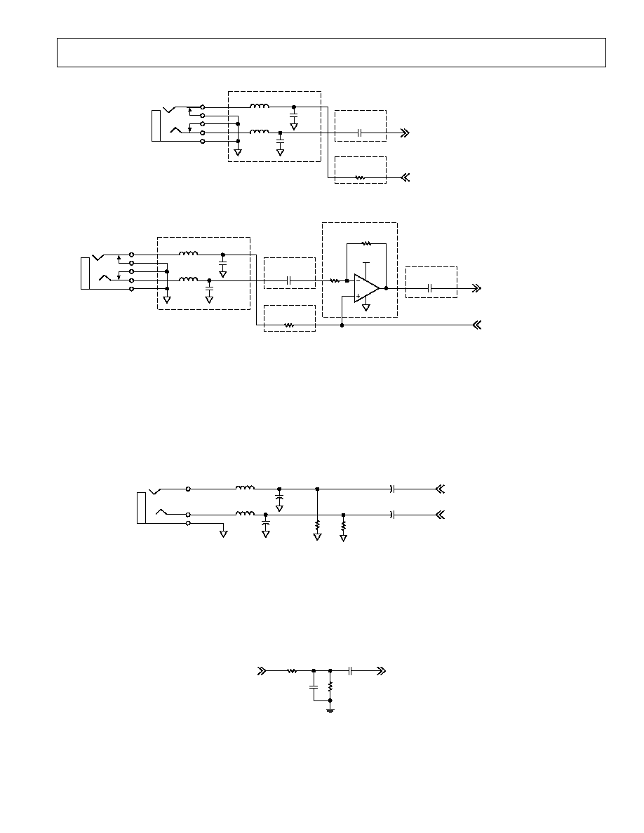
REV. 0
AD1886A
≠27≠
AC-COUPLING
TO CODEC MIC1 OR MIC2 INPUT
FROM CODEC V
REFOUT
MIC INPUT
1
2
3
4
5
J1
EMC
COMPONENTS
C1
470pF
C2
470pF
L2 600Z
L1 600Z
MIC BIAS
C3
0.22 F
R1
2.2k
Figure 16. Recommended Microphone Input Connections
TO CODEC MIC1 OR MIC2 INPUT
FROM CODEC V
REFOUT
AC-COUPLING
MIC INPUT
1
2
3
4
5
J1
EMC
COMPONENTS
C1
470pF
C2
470pF
L2 600Z
L1 600Z
MIC BIAS
AVDD
U1
PREAMP
AD8531
AC-COUPLING
C3
0.22 F
R1
2.2k
R3
100k
R2
10k
C4
0.22 F
Figure 17. Microphone with Additional External Preamp (20 dB Gain)
LINE OUTPUT CONNECTIONS
The AD1886A Codec provides stereo LINE_OUT signals at a standard 1 V rms level. These signals must be ac-coupled before they
can be connected to an external load. After the ac-coupling, a minimal resistive load is recommended to keep the capacitors properly
biased and reduce clicks and pops when plugging stereo equipment into the output jack. The capacitor values should be selected to
provide a desired frequency response, taking into account the nominal impedance of the external load. To meet the PC99 specifica-
tion for PCs, testing must be performed with a 10 k
load, therefore a minimum of 1 µF value is recommended to achieve less than
≠3 dB roll-off at 20 Hz.
FROM CODEC LINE_OUT_R
FROM CODEC LINE_OUT_L
J1
L1 600Z
L2 600Z
STEREO LINE_OUT JACK
C1
470pF
C2
470pF
C3
1 F
C4
1 F
R1
47k
R2
47k
Figure 18. Recommended LINE_OUT Connections
PC BEEP INPUT CONNECTIONS
The recommended PC BEEP input circuit is shown below. Under most cases the PC_BEEP signal should be attenuated, filtered and
then ac-coupled into the Codec.
TO CODEC PC_BEEP INPUT
PC_BEEP (FROM ICH)
R1
10k
C2
0.1 F
C1
0.1 F
R2
1k
Figure 19. Recommended PC_BEEP Connections

REV. 0
≠28≠
C02411≠0≠10/01(0)
PRINTED IN U.S.A.
AD1886A
OUTLINE DIMENSIONS
Dimensions shown in inches and (mm).
48-Lead Thin Plastic Quad Flatpack (LQFP)
(ST-48)
TOP VIEW
(PINS DOWN)
1
12
13
25
24
36
37
48
0.019 (0.5)
BSC
0.276
(7.00)
BSC
SQ
0.011 (0.27)
0.006 (0.17)
0.354 (9.00) BSC SQ
0.063 (1.60)
MAX
0.030 (0.75)
0.018 (0.45)
0.008 (0.2)
0.004 (0.09)
0
MIN
COPLANARITY
0.003 (0.08)
SEATING
PLANE
0.006 (0.15)
0.002 (0.05)
7
0
0.057 (1.45)
0.053 (1.35)
CONTROLLING DIMENSIONS ARE IN MILLIMETERS; INCH DIMENSIONS
ARE ROUNDED-OFF MILLIMETER EQUIVALENTS FOR REFERENCE
ONLY AND ARE NOT APPROPRIATE FOR USE IN DESIGN