 | –≠–ª–µ–∫—Ç—Ä–æ–Ω–Ω—ã–π –∫–æ–º–ø–æ–Ω–µ–Ω—Ç: AD1941 | –°–∫–∞—á–∞—Ç—å:  PDF PDF  ZIP ZIP |

SigmaDSP
TM
Multichannel
28-Bit Audio Processor
Preliminary Technical Data
AD1941
Rev. PrE
Information furnished by Analog Devices is believed to be accurate and reliable.
However, no responsibility is assumed by Analog Devices for its use, nor for any
infringements of patents or other rights of third parties that may result from its use.
Specifications subject to change without notice. No license is granted by implication
or otherwise under any patent or patent rights of Analog Devices. Trademarks and
registered trademarks are the property of their respective owners.
One Technology Way, P.O. Box 9106, Norwood, MA 02062-9106, U.S.A.
Tel: 781.329.4700
www.analog.com
Fax: 781.326.8703
© 2005 Analog Devices, Inc. All rights reserved.
FEATURES
16-channel digital audio processor
Accepts sample rates up to 192 kHz
28-bit ◊ 28-bit multiplier with full 56-bit accumulator
Fully-programmable program RAM for custom
program download
Parameter RAM allows complete control of 1,024 parameters
Control port features safeload for transparent parameter
updates and complete mode and memory transfer control
Target/slew RAM for click-free volume control and dynamic
parameter updates
Double precision mode for full 56-bit processing
PLL for generating MCLK from 64 ◊ f
S
, 256 ◊ f
S
, 384 ◊ f
S
, or
512 ◊ f
S
clocks
Hardware-accelerated DSP core
21 kB (6,144 words) data memory for up to 128 ms of audio
delay at f
s
= 48 kHz
Flexible serial data port with I
2
S compatible, left-justified,
and right-justified serial port modes
8- and 16-channel TDM input/output modes
On-chip voltage regulator for compatibility with 3.3 V and
5 V systems
Programmable low power mode
Fast start-up and boot time from power on or reset
48-lead LQFP plastic package
APPLICATIONS
Automotive sound systems
Digital televisions
Home theater systems (Dolby Digital/DTS postprocessor)
Multichannel audio systems
Mini-component stereos
Multimedia audio
Digital speaker crossover
Musical instruments
In-seat sound systems (aircrafts/motor coaches)
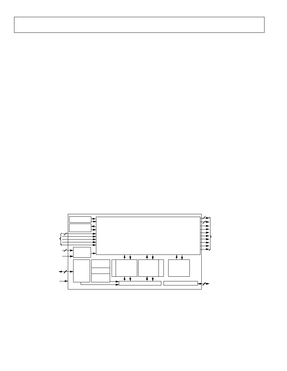
FUNCTIONAL BLOCK DIAGRAM
VOLTAGE
REGULATOR
AD1940
28
◊
28
DSP CORE
DATA FORMAT:
PLL
SERIAL
CONTROL
INTERFACE
SERIAL DATA/
TDM INPUTS
MASTER
CLOCK
INPUT
SPI I/O
RAM
ROM
SERIAL
DATA/
TDM
OUTPUTS
04607-0-001
2
4
4
2
2
5.23 (SINGLE
PRECISION)
10.46 (DOUBLE
PRECISION)
Figure 1.
GENERAL DESCRIPTION
The AD1941 is a complete 28-bit, single-chip, multichannel
audio DSP for equalization, multiband dynamics processing,
delay compensation, speaker compensation, and image
enhancement. These algorithms can be used to compensate for
the real-world limitations of speakers, amplifiers, and listening
environments, resulting in a dramatic improvement of
perceived audio quality.
The signal processing used in the AD1941 is comparable to that
found in high end studio equipment. Most of the processing is
done in full, 56-bit double-precision mode, resulting in very
good low level signal performance and the absence of limit
cycles or idle tones. The dynamics processor uses a sophisti-
cated, multiple-breakpoint algorithm often found in high end
broadcast compressors.
The AD1941 is a fully-programmable DSP. Easy to use software
allows the user to graphically configure a custom signal
processing flow using blocks such as biquad filters, dynamics
processors, and surround sound processors. An extensive
control port allows click-free parameter updates, along with
readback capability from any point in the algorithm flow.
The AD1941's digital input and output ports allow a glueless
connection to ADCs and DACs by multiple, 2-channel serial
data streams or TDM data streams. When in TDM mode, the
AD1941 can input 8 or 16 channels of serial data, and can
output either 8 or 16 channels of serial data. The input and
output port configurations can be individually set. The AD1941
is controlled on a 2-wire I
2
C bus.

AD1941
Preliminary Technical Data
Rev. PrE | Page 2 of 32
TABLE OF CONTENTS
Specifications..................................................................................... 3
Digital I/O ..................................................................................... 3
Power.............................................................................................. 3
Temperature Range ...................................................................... 3
Digital Timing............................................................................... 4
PLL ................................................................................................. 4
Regulator........................................................................................ 4
Absolute Maximum Ratings............................................................ 5
ESD Caution.................................................................................. 5
Digital Timing Diagrams................................................................. 6
Pin Configuration and Function Descriptions............................. 8
Features ............................................................................................ 10
Pin Functions .............................................................................. 11
Signal Processing ............................................................................ 13
Overview...................................................................................... 13
Numeric Formats........................................................................ 13
Programming .............................................................................. 13
Control Port..................................................................................... 14
Overview...................................................................................... 14
I
2
C Port ........................................................................................ 14
RAMs and Registers....................................................................... 16
Control Port Addressing............................................................ 16
Parameter RAM Contents......................................................... 16
Recommended Program/Parameter Loading Procedures.... 17
Target/Slew RAM ....................................................................... 17
Safeload Registers....................................................................... 19
Data Capture Registers .............................................................. 20
DSP Core Control Register ....................................................... 20
RAM Configuration Register ................................................... 21
Control Port Read/Write Data Formats .................................. 22
Serial Data Input/Output Ports .................................................... 24
Serial Output Control Registers ............................................... 26
Serial Input Control Register .................................................... 26
Initialization .................................................................................... 29
Power-Up Sequence ................................................................... 29
Setting Master Clock/PLL Mode.............................................. 29
Voltage Regulator ....................................................................... 29
Outline Dimensions ....................................................................... 30
Ordering Guide .......................................................................... 30

Preliminary Technical Data
AD1941
Rev. PrE | Page 3 of 32
SPECIFICATIONS
Test conditions, unless otherwise noted.
Table 1.
Parameter Conditions
Supply Voltage (VDD)
2.5 V
PLL Voltage (PLL_VDD)
2.5 V
Output Voltage (ODVDD)
5.0 V
INVDD Voltage
5.0 V
Ambient Temperature
25∞C
Master Clock Input
3.072 MHz, 64 ◊ f
s
mode
Load Capacitance
50 pF
Load Current
±1 mA
Input Voltage, HI
2.4 V
Input Voltage, LO
0.8 V
DIGITAL I/O
Table 2. Digital I/O
1
Parameter
Min
Max
Unit
Input Voltage, HI (V
IH
)
2.1
V
Input Voltage, LO (V
IL
)
0.8
V
Input Leakage (I
IH
)
10
µA
Input Leakage (I
IL
)
10
µA
High Level Output Voltage (V
OH
) ODVDD = 4.5 V, I
OH
= 1 mA
3.9
V
High Level Output Voltage (V
OH
) ODVDD = 3.0 V, I
OH
= 1 mA
2.6
V
Low Level Output Voltage (V
OL
) ODVDD = 4.5 V, I
OL
= 1 mA
0.4
V
Low Level Output Voltage (V
OL
) ODVDD = 3.0 V, I
OL
= 1 mA
0.3
V
Input Capacitance
5
pF
1
All measurements across -40∞C to 125∞C (case) and across VDD = 2.25 V to 2.75 V.
POWER
Table 3.
Parameter
Min
Typ
Max
1
Unit
Supplies
Voltage
2.25
2.5
2.75
V
Digital Current
92
155
2
mA
PLL Current
3.5
8
mA
Digital Current, Reset
4.5
3
13
3
mA
PLL Current, Reset
3
8.5
mA
Dissipation
Operation, all supplies
238.8
mW
Reset, all supplies
10.8
mW
1
Maximum specifications are measured across -40∞C to 125∞C (case) and across VDD = 2.25 V to 2.75 V.
2
Measurement running a typical large program that writes to all 16 outputs with 0 dB digital sine waves applied to all eight inputs. Your program may differ.
3
The digital reset current is specified for the given test conditions. This current scales with the input MCLK rate, so higher input clocks draw more current while in reset.
TEMPERATURE RANGE
Table 4.
Parameter
Min
Typ
Max
Unit
Functionality Guaranteed
≠40
+105
∞C Ambient
≠40
+125
∞C
Case
AD1941
Preliminary Technical Data
Rev. PrE | Page 4 of 32
DIGITAL TIMING
Table 5 Digital Timing
1
Parameter
Comments
Min
Max
Unit
t
MP
MCLK Period
512 f
S
mode
36
244
ns
t
MP
MCLK Period
384 f
S
mode
48
366
ns
t
MP
MCLK Period
256 f
S
mode
73
488
ns
t
MP
MCLK Period
64 f
S
mode
291
1953
ns
t
MP
MCLK Period
Bypass mode
12
ns
t
MDC
MCLK Duty Cycle
Bypass mode
40
60
%
t
BIL
BCLK_IN LO Pulse Width
4
ns
t
BIH
BCLK_IN HI Pulse Width
2
ns
t
LIS
LRCLK_IN Setup
To BCLK_IN rising
12
ns
t
LIH
LRCLK_IN Hold
From BCLK_IN rising
0
ns
t
SIS
SDATA_INx Setup
To BCLK_IN rising
3
ns
t
SIH
SDATA_INx Hold
From BCLK_IN rising
2
ns
t
LOS
LRCLK_OUTx Setup
Slave mode
2
ns
t
LOH
LRCLK_OUTx Hold
Slave mode
2
ns
t
TS
BCLK_OUTx Falling to
LRCLK_OUTx Timing Skew
2
ns
t
SODS
SDATA_OUTx Delay
Slave mode, from BCLK_OUTx falling
17
ns
t
SODM
SDATA_OUTx Delay
Master mode, from BCLK_OUTx falling
17
ns
t
RLPW
RESETB LO Pulse Width
10
ns
1
All timing specifications are given for the default (I
2
S) states of the serial input control port and the serial output control ports. See Table 32.
PLL
Table 6.
Parameter
Min
Typ
Max
Unit
Lock Time
3
20
ms
REGULATOR
Table 7.
Parameter
Min
Typ
Max
Unit
VSENSE Output Voltage
2.25
2.5
2.68
V
Preliminary Technical Data
AD1941
Rev. PrE | Page 5 of 32
ABSOLUTE MAXIMUM RATINGS
Table 8.
Parameter
Min
Max
Unit
VDD to DGND
≠0.3
+3.0
V
PLL_ VDD to PGND
≠0.3
+3.0
V
OD VDD to DGND
≠0.3
+6.0
V
INVDD to DGND
ODVDD
+6.0
V
Digital Inputs
DGND ≠ 0.3
INVDD + 0.3
V
Maximum Junction Temperature
135
∞C
Storage Temperature Range
≠65
+150
∞C
Soldering (10 sec)
300
∞C
Stresses above those listed under Absolute Maximum Ratings may cause permanent damage to the device. This is a stress rating only;
functional operation of the device at these or any other conditions above those indicated in the operational section of this specification is
not implied. Exposure to absolute maximum rating conditions for extended periods may affect device reliability.
Table 9. Package Characteristics
Parameter Min
Typ
Max
Unit
JA
Thermal Resistance (Junction-to-Ambient)
72
∞C/W
JC
Thermal Resistance (Junction-to-Case)
19.5
∞C/W
ESD CAUTION
ESD (electrostatic discharge) sensitive device. Electrostatic charges as high as 4000 V readily accumulate on
the human body and test equipment and can discharge without detection. Although this product features
proprietary ESD protection circuitry, permanent damage may occur on devices subjected to high energy
electrostatic discharges. Therefore, proper ESD precautions are recommended to avoid performance
degradation or loss of functionality.

AD1941
Preliminary Technical Data
Rev. PrE | Page 6 of 32
DIGITAL TIMING DIAGRAMS
BCLK_IN
LRCLK_IN
SDATA_INX
LEFT-JUSTIFIED
MODE
LSB
SDATA_INX
I
2
S-JUSTIFIED
MODE
SDATA_INX
RIGHT-JUSTIFIED
MODE
t
BIH
MSB
MSB-1
MSB
MSB
8-BIT CLOCKS
(24-BIT DATA)
12-BIT CLOCKS
(20-BIT DATA)
14-BIT CLOCKS
(18-BIT DATA)
16-BIT CLOCKS
(16-BIT DATA)
t
LIS
t
SIS
t
SIH
t
SIH
t
SIS
t
SIS
t
SIH
t
SIS
t
SIH
t
LIH
t
BIL
04607-0-013
Figure 2. Serial Input Port Timing
BCLK_OUTX
LRCLK_OUTX
SDATA_OUTX
LEFT-JUSTIFIED
MODE
LSB
SDATA_OUTX
I
2
S-JUSTIFIED
MODE
SDATA_OUTX
RIGHT-JUSTIFIED
MODE
t
BIH
MSB
MSB-1
MSB
MSB
8-BIT CLOCKS
(24-BIT DATA)
12-BIT CLOCKS
(20-BIT DATA)
14-BIT CLOCKS
(18-BIT DATA)
16-BIT CLOCKS
(16-BIT DATA)
t
LOS
t
SDDS
t
SDDM
t
SDDS
t
SDDM
t
SDDS
t
SDDM
t
LCH
t
TS
t
BIL
04607-0-014
Figure 3. Serial Output Port Timing
Preliminary Technical Data
AD1941
Rev. PrE | Page 7 of 32
MCLK
RESETB
t
MP
t
RLPW
04607-0-016
Figure 4. Master Clock and Reset Timing

AD1941
Preliminary Technical Data
Rev. PrE | Page 8 of 32
PIN CONFIGURATION AND FUNCTION DESCRIPTIONS
36
35
34
33
32
31
30
29
28
27
26
25
13 14 15 16 17 18 19 20 21 22 23 24
1
2
3
4
5
6
7
8
9
10
11
12
48 47 46 45 44
39 38 37
43 42 41 40
GND
BCLK_OUT1
LRCLK_OUT1
ODVDD
SDATA_OUT3
SDATA_OUT2
SDATA_OUT1
VDD
MCLK
RESERVED
PLL_VDD
I2C_FILT_EN
SDATA_OUT0
ODVDD
BCLK_OUT0
LRCLK_OUT0
GND
VDD
PIN 1
INDICATOR
PLL_CTRL0
PLL_CTRL1
PLL_CTRL2
PLL_GND
AD1941
TOP VIEW
(Not to Scale)
V
D
D
S
D
A
T
A
_
I
N
1
S
D
A
T
A
_
I
N
2
S
D
A
T
A
_
I
N
3
S
D
A
S
C
L
N
C
N
C
R
E
S
E
T
B
G
N
D
S
DATA_
IN0
ADR_
S
E
L
GND
VR
EF
VD
R
IVE
V
SE
NS
E
VSU
PP
LY
INV
DD
S
DATA
_
OUT7
SD
A
TA
_
O
UT6
ODVDD
SD
A
TA
_
O
UT5
S
DATA
_O
UT
4
VD
D
04607-0-011
LRCLK_IN
BCLK_IN
NC = NO CONNECT
Figure 5. 48-Lead LQFP Pin Configuration, AD1941
Table 10. Pin Function Descriptions
Pin No.
I/O
Mnemonic
Description
1, 25, 37
VDD
Core Power.
2
IN
MCLK
Master Clock Input.
3, 21, 22
RESERVED
These pins should be connected to ground.
4
IN
PLL_CTRL0
PLL Control 0.
5
IN
PLL_CTRL1
PLL Control 1.
6
IN
PLL_CTRL2
PLL Control 2.
7
PLL_GND
PLL Ground.
8
PLL_VDD
PLL Power.
9 IN
I2C_FILT_ENB
I
2
C Filter Enable, Active Low.
10
IN
LRCLK_IN
Left/Right Clock for Serial or TDM Data Inputs.
11
IN
BCLK_IN
Bit Clock for Serial or TDM Data Inputs.
12, 24, 36, 48
GND
Digital Ground.
13
VDD
Core Power.
14
IN
SDATA_IN0
Serial Data Input 0.
12
IN
SDATA_IN1
Serial Data Input 1.
16 IN
SDATA_IN2/TDM_IN1
Serial Data Input 2/TDM Input 1.
17 IN
SDATA_IN3/TDM_IN0
Serial Data Input 3/TDM Input 0.
18
IN
ADR_SEL
Control Port Address Select.
19 IN/OUT
SDA
I
2
C Serial Data I/O.
20 IN
SCL
I
2
C Clock.
23
IN
RESETB
Reset the AD1941.
26
IN/OUT
LRCLK_OUT0
Left/Right Clock Output 0.
27
IN/OUT
BCLK_OUT0
Bit Clock Output 0.
28, 33, 40
ODVDD
Power connection for Output Pins.
29
OUT
SDATA_OUT0/TDM_O0
Serial Data Output 0/TDM (16- or 8-Channel) Output 0
30
OUT
SDATA_OUT1
Serial Data Output 1.
31
OUT
SDATA_OUT2
Serial Data Output 2.
32
OUT
SDATA_OUT3
Serial Data Output 3.
Preliminary Technical Data
AD1941
Rev. PrE | Page 9 of 32
Pin No.
I/O
Mnemonic
Description
34
IN/OUT
LRCLK_OUT1
Left/Right Clock Output 1.
35
IN/OUT
BCLK_OUT1
Bit Clock Output 1.
38
OUT
SDATA_OUT4/TDM_O1
Serial Data Output 4./TDM (8-Channel) Output 1
39
OUT
SDATA_OUT5
Serial Data Output 5.
41
OUT
SDATA_OUT6
Serial Data Output 6.
42
OUT
SDATA_OUT7/DCSOUT
Serial Data Output 7/Data Capture Output.
43
INVDD
Input Voltage Reference.
44
IN
VSUPPLY
Voltage Level Input to Regulator. Usually 3.3 V or 5 V.
45
IN
VSENSE
Digital Power Level. Should be tied to VDD.
46
OUT
VDRIVE
Drive for External PNP Transistor.
47
OUT
VREF
Reference Level for Voltage Regulator.
AD1941
Preliminary Technical Data
Rev. PrE | Page 10 of 32
FEATURES
The core of the AD1941 is a 28-bit DSP (56-bit with double
precision) optimized for audio processing.
The AD1941 contains a program RAM that is initialized from
an internal program ROM on power-up. The program RAM
can be loaded with a custom program after power-up. Signal
processing parameters are stored in a 1024-location parameter
RAM, which is initialized on power-up by an internal boot-
ROM. New values are written to the parameter RAM using the
control port. The values stored in the parameter RAM control
individual signal processing blocks, such as IIR equalization
filters, dynamics processors, audio delays, and mixer levels. A
safeload feature allows parameters to be transparently updated
without causing clicks on the output signals.
The target/slew RAM contains 64 locations and can be used as
channel volume controls or for other parameter updates. These
RAM locations take a target value for a given parameter and
ramp the current parameter value to the new value using a
specified time constant and one of a selection of linear or
logarithmic curves.
The AD1941 has a sophisticated control port that supports
complete read/write capability of all memory locations. Five
control registers (core, RAM configuration, Serial Output 0 to 7,
Serial Output 8 to 15, and serial input) are provided to offer
complete control of the chip's configuration and serial modes.
Handshaking is included for ease of memory
uploads/downloads.
The AD1941 contains eight independent data capture circuits
that can be programmed to tap the signal flow of the processor
at any point in the DSP algorithm flow. Six of these captured
signals can be accessed by reading from the data capture
registers through the control port. The remaining two data
capture registers can be used to send any internal captured
signal to a stereo digital output signal on Pin SDATA_OUT7 for
driving external DACs or digital analyzers.
The AD1941 has very flexible serial data input/output ports that
allows for glueless interconnection to a variety of ADCs, DACs,
general-purpose DSPs, S/PDIF receivers, and sample rate
converters. The AD1941 can be configured in I
2
S, left-justified,
right-justified, or TDM serial port compatible modes. It can
support 16, 20, and 24 bits in all modes. The AD1941 accepts
serial audio data in MSB first and twos complement format.
The AD1941 operates from a single 2.5 V power supply. It is
fabricated on a single monolithic integrated circuit and is
housed in a 48-lead LQFP package for operation over the
≠40∞C to +105∞C temperature range.
04607-0-003
28
◊
28
DSP CORE
DATA FORMAT:
5.23 (SINGLE PRECISION)
10.46 (DOUBLE PRECISION)
VOLTAGE REGULATOR
MEMORY CONTROLLERS
CONTROL
REGISITER
TRAP REG.
SAFELOAD
REGISTER
SERIAL
CONTROL
PORT
MCLK
PLL
DATA MEMORY
6k
◊
28
TARGET/SLEW
RAM
64
◊
28
SERIAL
DATA/TDM
INPUT
GROUP
PLL MODE
SELECT
MASTER
CLOCK
INPUT
SPI I/O
GROUP
RESETB
PROGRAM
RAM
1536
◊
40
BOOT ROM
BOOT ROM
PARAMETER
RAM
1024
◊
28
COEFFICIENT
ROM
512
◊
28
2
2
4
4
2
2
SERIAL DATA/
TDM OUTPUT
GROUP
REGULATOR
GROUP
Figure 6. Block Diagram

Preliminary Technical Data
AD1941
Rev. PrE | Page 11 of 32
PIN FUNCTIONS
Table 10 shows the AD1941's pin numbers, names, and
functions. Input pins have a logic threshold compatible with
TTL input levels and may be used in systems with 3.3 V or
5 V logic.
SDATA_IN0
SDATA_IN1
SDATA_IN2/TDM_IN1
SDATA_IN3/TDM_IN0
Serial Data/TDM Inputs. The serial format is selected by writing
to Bits 2:0 of the serial input port control register. SDATA_IN2
and SDATA_IN3 are dual-function pins that can be set to a
variety of standard 2-channel formats or to TDM mode. Two of
these four pins (SDATA_IN2 and SDATA_IN3) can be used as
TDM inputs in either dual-wire 8-channel mode or single-wire
16-channel mode (TDM_O0 only). In dual-wire 8-channel
mode, Channels 0-7 will be input on SDATA_IN3 and
Channels 8-15 on SDATA_IN2. In single-wire 16-channel
mode, Channels 0-15 will be input on SDATA_IN2. See the
Serial Data Input/Output Ports section for further explanation.
LRCLK_IN
BCLK_IN
Left/Right and Bit Clocks for Timing the Input Data. These
input clocks are associated with the SDATA_IN0-3 signals. The
input port is always in a slave configuration. These pins also
function as frame sync and bit clock for the input TDM stream.
SDATA_OUT0/TDM_O0
SDATA_OUT1
SDATA_OUT2,
SDATA_OUT3
SDATA_OUT4/TDM_O1
SDATA_OUT5
SDATA_OUT6
SDATA_OUT7/DCSOUT
Serial Data/TDM/Data Capture Outputs. These pins are used
for serial digital outputs. For non-TDM systems, these eight
pins can output 16 channels of digital audio, using a variety of
standard two-channel formats. They are grouped into two
groups of four pins (0-3 and 4-7); each group can be indepen-
dently set to any of the available serial modes, allowing the
AD1941 to simultaneously communicate with two external
devices with different serial formats. Two of these eight pins
(SDATA_OUT0 and SDATA_OUT4) can be used as TDM
outputs in either dual-wire 8-channel mode or single-wire
16-channel mode (TDM_OUT0 only). In dual-wire 8-channel
mode, Channels 0-7 will be output on SDATA_OUT0 and
Channels 8-15 on SDATA_OUT4. See the Serial Data
Input/Output Ports section for further explanation.
SDATA_OUT7 can also be used as a data capture output, as
described in the Data Capture Registers section.
LRCLK_OUT0
BCLK_OUT0
Output Clocks. This clock pair is used for outputs
SDATA_OUT0≠3. In slave mode, these clocks are inputs
to the AD1941. On power-up, these pins are set to slave
mode to avoid conflicts with external master-mode devices.
LRCLK_OUT1
BCLK_OUT1
Output Clocks. This clock pair is used for outputs
SDATA_OUT4≠7. In slave mode, these clocks are inputs
to the AD1941. On power-up, these pins are set to slave
mode to avoid conflicts with external master-mode devices.
MCLK
Master Clock Input. The AD1941 uses a PLL to generate the
appropriate internal clock for the DSP core. An in-depth
description of using the PLL is found in the Setting Master
Clock/PLL Mode section.
PLL_CTRL0
PLL_CTRL1
PLL_CTRL2
PLL Mode Control Pins. The functionality of these pins is
described in the Setting Master Clock/PLL Mode section.
SCL
I
2
C Clock. This pin is always an input because the AD1941
cannot act as a master on the I
2
C bus. The line connected to this
pin should have a 2 k pull-up resistor on it.
SDA
I
2
C Serial Data. The data line is bidirectional. The line
connected to this pin should have a 2 k pull-up resistor on it.
I2C_FILT_ENB
I
2
C Spike Filter Enable/Disable. This enables (active low) the I
2
C
spike filter, which is used to prevent noise or glitches on the I
2
C
bus, from improperly affecting the AD1941.
ADR_SEL
Address Select. This pin selects the address for the AD1941's
communication with the control port. This allows two AD1941s
to be used with a single CLATCH signal.
RESETB
Active-Low Reset Signal. After RESETB goes high, the AD1941
goes through an initialization sequence where the program and
parameter RAMs are initialized with the contents of the on-
board boot ROMs. All registers are set to 0, and the data RAMs
are also set to 0. The initialization is complete after
8,192 internal MCLK cycles (referenced to the rising edge of
RESETB), which corresponds to 1,366 external MCLK cycles if
the part is in 256 ◊ f
S
mode. New values should not be written to
the control port until the initialization is complete.

AD1941
Preliminary Technical Data
Rev. PrE | Page 12 of 32
VREF
Voltage Reference for Regulator. This pin is driven by an
internal 1.15 V reference voltage.
VDRIVE
Drive for External Transistor. The base of the voltage regulator's
external PNP transistor is driven from this pin.
VSENSE
Digital power level. The voltage level on the VDD pins is sensed
on VSENSE. VSENSE should be tied to VDD.
VSUPPLY
Main Supply Voltage Level. This pin is tied to the board's main
voltage supply. This is usually 3.3 V or 5 V.
VDD (4)
Digital VDD for Core. 2.5 V nominal.
GND (4)
Digital Ground.
PLL_VDD
Supply for AD1941 PLL. 2.5 V nominal.
PLL_GND
PLL Ground.
ODVDD (3)
VDD for All Digital Outputs. The high levels of the digital
output signals are set on this pin. The voltage can range from
2.5 V to 5.0 V.
INVDD
Peak Input Voltage Level. The highest voltage level that the
input pins will see should be connected to INVDD. This is to
protect the chip inputs from voltage overstress. The voltage on
this pin must always be at or above the level of ODVDD.

Preliminary Technical Data
AD1941
Rev. PrE | Page 13 of 32
SIGNAL PROCESSING
OVERVIEW
The AD1941 is designed to provide all signal processing
functions commonly used in stereo or multichannel playback
systems. The signal processing flow is set by using the ADI-
supplied software, which allows graphical entry and real-time
control of all signal processing functions.
Many of the signal processing functions are coded using full,
56-bit double-precision arithmetic. The input and output word
lengths are 24 bits. Four extra headroom bits are used in the
processor to allow internal gains up to 24 dB without clipping.
Additional gains can be achieved by initially scaling down the
input signal in the signal flow.
The signal processing blocks can be arranged in a custom pro-
gram that can be loaded to the AD1941's RAM. The available
signal processing blocks are explained in the following sections.
NUMERIC FORMATS
It is common in DSP systems to use a standardized method of
specifying numeric formats. Fractional number systems are
specified by an A.B format, where A is the number of bits to the
left of the decimal point and B is the number of bits to the right
of the decimal point.
The AD1941 uses the same numeric format for both the coeffi-
cient values (stored in the parameter RAM) and the signal data
values. The format is as follows:
Numerical Format: 5.23
Range: ≠16.0 to (+16.0 - 1 LSB)
Examples:
1000000000000000000000000000 = ≠16.0
1110000000000000000000000000 = ≠4.0
1111100000000000000000000000 = ≠1.0
1111111000000000000000000000 = ≠0.25
1111111111111111111111111111 = (1 LSB below 0.0)
0000000000000000000000000000 = 0.0
0000001000000000000000000000 = 0.25
0000100000000000000000000000 = 1.0
0010000000000000000000000000 = 4.0
0111111111111111111111111111 = (16.0 ≠ 1 LSB).
The serial port accepts up to 24 bits on the input and is sign-
extended to the full 28 bits of the core. This allows internal
gains of up to 24 dB without encountering internal clipping.
A digital clipper circuit is used between the output of the DSP
core and the serial output ports (see Figure 7). This clips the top
four bits of the signal to produce a 24-bit output with a range of
1.0 (minus 1 LSB) to ≠1.0.
4-BIT SIGN EXTENSION
DATA IN
SERIAL PORT
1.23
5.23
SIGNAL PROCESSING
(5.23 FORMAT)
DIGITAL
CLIPPER
5.23
1.23
04607-0-005
Figure 7. Numeric Precision and Clipping Structure
PROGRAMMING
On power-up, the AD1941's default program passes the unpro-
cessed input signals to the outputs but the outputs come up
muted by default (see Power-Up Sequence section). There are
1,536 instruction cycles per audio sample, resulting in an inter-
nal clock rate of 73.728 MHz (for f
s
= 48 kHz). This DSP runs in
a stream-oriented manner, meaning all 1,536 instructions are
executed each sample period. The AD1941 may also be set
up to accept double or quad-speed inputs by reducing the
number of instructions/sample, which can be set in the core
control register.
The part can be programmed easily using graphical tools pro-
vided by Analog Devices. No knowledge of writing DSP code is
needed to program this part. The user can simply connect
graphical blocks such as biquad filters, dynamics processors,
mixers, and delays in a signal flow schematic, compile the
design, and load the program and parameter files into the
AD1941's Program RAM through the control port. Signal
processing blocks available in the provided libraries include
∑
Single- and double-precision biquad filters
∑
Mono and multichannel dynamics processors
∑
Mixers and splitters
∑
Tone and noise generators
∑
First-order filters
∑
Fixed and variable gain
∑
RMS look-up tables
∑
Loudness
∑
Delay
∑
Stereo enhancement (Phat StereoTM)
∑
Interpolators and Decimators
More blocks are always in development. Analog Devices also
provides proprietary and third-party algorithms for applications
such as matrix decoding, bass enhancement, and surround
virtualizers. Please contact ADI for information about licensing
these algorithms.

AD1941
Preliminary Technical Data
Rev. PrE | Page 14 of 32
CONTROL PORT
OVERVIEW
The AD1941 has many different control options that can be set
through an I
2
C interface. Most signal processing parameters are
controlled by writing new values to the parameter RAM using the
control port. Other functions, such as mute and input/ output
mode control, are programmed by writing to the control registers.
The control port is capable of full read/write operation for all of
the memories and registers. All addresses may be accessed in
both a single-address mode or a burst mode. A control word
consists of the chip address, the register/RAM subaddress, and
the data to be written. The data can be variable in its byte width.
The first byte of a control word (Byte 0) contains the 7-bit chip
address plus the R/W bit. The next two bytes (Bytes 1 and 2)
together form the subaddress of the memory or register
location within the AD1941. This subaddress needs to be two
bytes because the memories within the AD1941 are directly
addressable, and their sizes exceed the range of single-byte
addressing. All subsequent bytes (Bytes 3, 4, etc.) contain the
data, such as control port data or program or parameter data.
The AD1941 has several mechanisms for updating signal
processing parameters in real time without causing pops or
clicks. In cases where large blocks of data need to be down-
loaded, the output of the DSP core can be halted (using Bit 9 of
the core control register), new data loaded, and then restarted.
This is typically done during the booting sequence at start-up or
when loading a new program into RAM. In cases where only a
few parameters need to be changed, they can be loaded without
halting the program. To avoid unwanted side effects while
loading parameters on the fly, the SigmaDSP provides the
safeload registers. The safeload registers can be used to buffer a
full set of parameters (e.g. the five coefficients of a biquad) and
then transfer these parameters into the active program within
one audio frame. The safeload mode uses internal logic to
prevent contention between the DSP core and the control port.
I
2
C PORT
The AD1941 supports a 2-wire serial (I
2
C compatible) micro-
processor bus driving multiple peripherals. Two inputs, serial
data (SDA) and serial clock (SCL), carry information between
the AD1941 and the system I
2
C master controller. The AD1941
is always a slave on the I
2
C bus, which means that it will never
initiate a data transfer. Each slave device is recognized by a
unique address. The AD1941 has four possible slave addresses,
two for writing operations and two for reading. These are
unique addresses for the device and are illustrated in Table 11.
The LSB of the byte sets either a read or write operation; Logic
Level 1 corresponds to a read operation, and Logic Level 0
corresponds to a write operation. The seventh bit of the address
is set by tying the ADR_SEL pin of the AD1941 to Logic Level 0
or Logic Level 1.
The AD1941 I
2
C port uses a spike filter which can be enabled or
disabled by the I2C_FILT_ENB pin. Enabling this filter
guarantees that all isolated spikes, both positive and negative,
less than 50 ns wide will be removed from the I
2
C signal. The
filter is active when the I2C_FILT_ENB pin is low, and is
disabled when the pin is at a high logic level.
Table 11. I
2
C Address for AD1941
ADR_SEL R/W
Slave
Address
0 0
0x28
0 1
0x29
1 0
0x2A
1 1
0x2B
Initially, all devices on the I
2
C bus are in an idle state, which is
where the devices monitor the SDA and SCL lines for a start
condition and the proper address. The I
2
C master initiates a
data transfer by establishing a Start condition, defined by a
high-to-low transition on SDA while SCL remains high. This
indicates that an address/data stream will follow. All devices on
the bus respond to the start condition and shift the next eight
bits (7-bit address + R/W bit) MSB first. The device that
recognizes the transmitted address responds by pulling the data
line low during the ninth clock pulse. This ninth bit is known as
an acknowledge bit. All other devices withdraw from the bus at
this point and return to the idle condition. The R/W bit
determines the direction of the data. A logic 0 on the LSB of the
first byte means the master will write information to the
peripheral. A logic 1 on the LSB of the first byte means the
master will read information from the peripheral. A data
transfer takes place until a stop condition is encountered. A stop
condition occurs when SDA transitions from low to high while
SCL is held high. Figure 8 shows the timing of a single-byte I
2
C
write.
Burst mode addressing, where the subaddresses are automati-
cally incremented at word boundaries, can be used for writing
large amounts of data to contiguous memory locations. This
increment happens automatically if a stop condition is not
encountered after a single-word write. The registers and
memories in the AD1941 range in width from one to five bytes,
so the autoincrement feature knows the mapping between sub-
addresses and the word length of the destination register (or
memory location). A data transfer is always terminated by a
stop condition.
Stop and start conditions can be detected at any stage during
the data transfer. If these conditions are asserted out of
sequence with normal read and write operations, these cause an
immediate jump to the idle condition. During a given SCL high
period, the user should only issue one start condition, one stop
condition, or a single stop condition followed by a single start

Preliminary Technical Data
AD1941
Rev. PrE | Page 15 of 32
condition. If an invalid subaddress is issued by the user, the
AD1941 does not issue an acknowledge and returns to the idle
condition. If the user exceeds the highest subaddress while in
autoincrement mode, one of two actions will be taken. In read
mode, the AD1941 outputs the highest subaddress register
contents until the master device issues a no-acknowledge,
indicating the end of a read. A no-acknowledge condition is
where the SDA line is not pulled low on the ninth clock pulse
on SCL. If the highest subaddress location is reached while in
write mode, the data for the invalid byte is not loaded into any
subaddress register, a no-acknowledge is issued by the AD1941,
and the part returns to the idle condition.
I
2
C Register/Memory Write Operation
Figure 9 shows the timing of a single-word write operation.
Every ninth clock, the AD1941 issues an acknowledge by
pulling its data line low.
Figure 10 shows the timing of a burst mode write sequence.
This figure shows an example where the target destination
registers are two bytes. The AD1941 knows to increment its sub-
address register every two bytes because the requested
subaddress corresponds to a register or memory area with a
2-byte word length.
The timing of a single word read operation is shown in
Figure 11. Note that the first R/W bit is still a 0, indicating a
write operation. This is because the subaddress still needs to be
written in order to set up the internal address. After the AD1941
acknowledges the receipt of the subaddress, the master must
issue a repeated start command followed by the chip address
byte with the R/W set to 1 (read). This causes the AD1941's
SDA to turn around and begin driving data back to the master.
The master then responds every ninth pulse with an
acknowledge pulse to the AD1941.
Figure 12 shows the timing of a burst-mode read sequence. This
figure shows an example where the target read registers are two
bytes. The AD1941 knows to increment its subaddress register
every two bytes because the requested subaddress corresponds
to a register or memory area with word lengths of two bytes.
Other address ranges may have a variety of word lengths
ranging from one to five bytes; the AD1941 always decodes the
subaddress and sets the autoincrement circuit so that the
address increments after the appropriate number of bytes.
1≠7
8
9
1≠7
8
9
1≠7
8
9
1≠7
8
9
START ADDR
R/W
ACK
ACK
SUBADDR LOW
SUBADDR HI
ACK
DATA [7:0]
ACK
S
P
SDA
SCL
8
STOP
04607-0-010
Figure 8. Single Byte I
2
C Write Timing
S Chip
Address,
R/W = 0
AS Subaddress
high
AS Subaddress
low
AS Data
0,
Byte 1
AS Data
0,
Byte 2
... AS Data
0,
Byte N
P
Figure 9. Single-Word I
2
C Write
S Chip
Address,
R/W = 0
AS Subaddress
high
AS Subaddress
low
AS Data
0,
Byte 1
AS Data
0,
Byte 2
AS Data
1,
Byte 1
AS Data
1,
Byte 2
AS ...
First Word
Second Word
P
Figure 10. Burst Mode I
2
C Write
S Chip
Address,
R/W = 0
AS Subaddress
high
AS Subaddress
low
AS S Chip
Addr,
R/W = 1
AS Data
0, Byte
1
AM Data
0, Byte
2
... AM Data
0,
Byte N
P
Figure 11. Single Word I
2
C Read
S Chip
Address,
R/W = 0
AS Subaddress
high
AS Subaddress
low
AS S Chip
Address,
R/W = 1
AS Data
0,
Byte 1
AM Data
0,
Byte 2
...
First Word
AM
P
Figure 12. Burst Mode I
2
C Read
S = Start Bit A(S) = Acknowledge by Slave
P = Stop Bit A(M) = Acknowledge by Master
AD1941
Preliminary Technical Data
Rev. PrE | Page 16 of 32
RAMS AND REGISTERS
Table 12. Control Port Addresses
SPI Address
Register Name
Read/Write Word Length
0≠1023 (0x0000≠0x03FF)
Parameter RAM
Write: 4 Bytes, Read: 4 Bytes
1024≠2559 (0x0400≠0x09FF)
Program RAM
Write: 5 Bytes, Read: 5 Bytes
2560≠2623 (0x0A00≠0x0A3F)
Target/Slew RAM
Write: 5 Bytes, Read: N/A
2624≠2628 (0x0A40≠0x0A44)
Parameter RAM Data Safeload Registers 0≠4
Write: 5 Bytes, Read: N/A
2629≠2633 (0x0A45≠0x0A49)
Parameter RAM Indirect Address Safeload Registers 0-4
Write: 2 Bytes, Read: N/A
2634≠2639 (0x0A4A≠0x0A4F)
Data Capture Registers 0≠5 (Control Port Readback)
Write: 2 Bytes, Read: 3 Bytes
2640≠2641 (0x0A50≠0x0A51)
Data Capture Registers (Digital Output)
Write: 2 Bytes, Read: N/A
2642 (0x0A52)
DSP Core Control Register
Write: 2 Bytes, Read: 2 Bytes
2643 (0x0A53)
RAM Configuration Register
Write: 1 Byte, Read: 1 Byte
2644 (0x0A54)
Serial Output Control Register 1 (Channels 0≠7)
Write: 2 Bytes, Read: 2 Bytes
2645 (0x0A55)
Serial Output Control Register 2 (Channels 8≠15)
Write: 2 Bytes, Read: 2 Bytes
2646 (0x0A56)
Serial Input Control Register
Write: 1 Byte, Read: 1 Byte
Table 13. RAM Read/Write Modes
Memory Size
SPI Address
Range
Read
Write
Burst Mode
Available? Write
Modes
Parameter RAM
1024 ◊ 28
0≠1023
(0x0000≠0x03FF)
Yes Yes
Yes
Direct
Write
1
Safeload Write
Program RAM
1536 ◊ 40
1024≠2559
(0x0400≠0x09FF)
Yes Yes
Yes
Direct
Write
1
Target/Slew RAM
64 ◊ 34
2560≠2623
(0x0A00≠0x0A3F)
No
Yes (via
Safeload)
Yes
2
Safeload
Write
1
DSP core should be shut down first to avoid clicks/pops.
2
The target/slew RAMs need to be written through the safeload registers. Safeload writes may be done in either single-write or burst-mode.
CONTROL PORT ADDRESSING
Table 12 shows the addressing of the AD1941's RAM and
register spaces. The address space encompasses a set of registers
and three RAMs: one each for holding signal processing
parameters, holding the program instructions, and ramping
parameter values. The program and parameter RAMs are
initialized on power-up from on-board boot ROMs.
Table 13 shows the sizes and available writing modes of the
parameter, program, and target/slew RAMs.
PARAMETER RAM CONTENTS
The parameter RAM is 28 bits wide and occupies Addresses 0 to
1023. The parameter RAM is initialized to all 0s on power-up.
The data format of the parameter RAM is twos complement
5.23. This means that the coefficients may range from +16.0
(minus 1 LSB) to ≠16.0, with 1.0 represented by the binary word
0000100000000000000000000000.
Options for Parameter Updates
The parameter RAM can be written and read using one of the
two following methods.
1.
Direct Read/Write
. This method allows direct access to the
program and parameter RAMs. This mode of operation is
normally used during a complete new load of the RAMs,
using burst-mode addressing. The clear registers bit in the
core control register should be set to 0 using this mode to
avoid any clicks or pops in the outputs. Note that it is also
possible to use this mode during live program execution,
but since there is no handshaking between the core and the
control port, the parameter RAM will be unavailable to the
DSP core during control writes, resulting in clicks and pops
in the audio stream.
2.
Safeload Writes.
Up to five safeload registers can be loaded
with address/data intended for the parameter RAM. The
data is then transferred to the requested address when the
RAM is not busy. This method can be used for dynamic
updates while live program material is playing through the
AD1941/AD1941. For example, a complete update of one
biquad section can occur in one audio frame, while the
RAM is not busy. This method is not available for writing
to the program RAM or control registers.
The following section discusses these two options in more
detail.
Preliminary Technical Data
AD1941
Rev. PrE | Page 17 of 32
RECOMMENDED PROGRAM/PARAMETER
LOADING PROCEDURES
When writing large amounts of data to the program or para-
meter RAM in direct write mode, the processor core should be
disabled to prevent unpleasant noises from appearing at the
audio output. The AD1941 contains several mechanisms for
disabling the core.
If the loaded program does NOT use the target/slew RAM as
the main system volume control (for example, the default
power-up program)
1.
Assert Bit 9 (LOW to assert--default setting) and Bit 6
(HIGH to assert) of the core control register. This zeroes
the accumulators, the serial output registers, and the serial
input registers.
2.
Fill the program RAM using burst mode writes.
3.
Fill the parameter RAM using burst mode writes.
4.
Assert Bit 7 of the core control register to initiate a data-
memory clear sequence. Wait at least 100 µs for this
sequence to complete. This bit is automatically cleared after
the operation is complete.
5.
Deassert Bit 9 and Bit 6 of the core control register to allow
the core to begin normal operation
If the loaded program does use the target/slew RAM as the
main system volume control:
1.
Assert Bit 12 of the core control register. This begins a
volume ramp-down, with a time constant determined by
the upper bits of the target RAM. Wait for this ramp-down
to complete (the user may poll Bit 13 of the core control
register, or simply wait for a given amount of time).
2.
Assert Bit 9 (LOW to assert) and Bit 6 (HIGH to assert) of
the core control register. This zeroes the accumulators, the
serial output registers, and the serial input registers.
3.
Fill the program RAM using burst-mode writes.
4.
Fill the parameter RAM using burst-mode writes.
5.
Assert Bit 7 of the core control register to initiate a data-
memory clear sequence. Wait at least 100 µs for this
sequence to complete. This bit is automatically cleared after
the operation is complete.
6.
Deassert Bit 9 and Bit 6 of the core control register.
7.
If the newly loaded program also uses the target/slew
RAM, deassert Bit 12 of the core control register to begin a
volume ramp-up procedure.
TARGET/SLEW RAM
The target/slew RAM is a bank of 64 RAM locations, each of
which can each be set to autoramp from one value to a desired
final value in one of four modes.
Summary
The target/slew RAM is used by the DSP when a program is
loaded into the program RAM that uses one or more locations
in the slew RAM to access internal coefficient data. Typically,
these coefficients are used for volume controls or smooth cross-
fading effects, but may be used to update any value in the para-
meter RAM. Each of the 64 locations in the slew RAM are
linked to corresponding locations in the target RAM. When a
new value is written to the target RAM using the control
port, the corresponding slew RAM location begins to ramp
toward the target. The value is updated once per audio frame
(LRCLK period).
The target RAM is 34 bits wide. The lower 28 bits contain the
target data in 5.23 format for the linear and exponential
(constant dB and RC-type) ramp types. For constant time
ramping, the lower 28 bits contain 16 bits in 2.14 format and 12
bits to set the current step. The upper six bits are used to
determine the type and speed of the ramp envelope in all
modes. The format of the data write for linear and exponential
formats is shown in Table 14. Table 15 shows the data write
format for the constant time ramping.
Data can only be written to the target/slew RAM using the
safeload registers as described in the Safeload Registers section.
A mute slew RAM bit is included in the core control register to
simultaneously set all the slew RAM target values to 0. This is
useful for implementing a global multichannel mute. When this
bit is deasserted, all slew RAM values will return to their
original pre-muted states.
Table 14. Linear, Constant dB, and RC-type
Ramp Data Write
Byte 0
Byte 1
Bytes 2≠4
000000,
curve_type[1:0]
time_const[3:0],
data[27:24]
data[23:0]
Table 15. Constant Time Ramp Data Write
Byte 0
Byte 1
Bytes 2≠4
000000,
curve_type[1:0]
update_step[0],
#_of_steps[2:0], data[15:12]
data[11:0],
reserved[11:0]
AD1941
Preliminary Technical Data
Rev. PrE | Page 18 of 32
The four ramping curve types are
1.
Linear--Value slews to target using a fixed step size.
2.
Constant dB--Value slews to target using the current value
to calculate the step size. The resulting curve has a constant
rise and decay when measured in dB.
3.
RC-type--Value slews to target using the difference
between target and current values to calculate the step size,
producing a simple RC type curve for rising and falling.
4.
Constant Time--Value slews to the target in a fixed
number of steps in a linear fashion. The control port mute
has no affect on this type.
Table 16 Target/Slew RAM Ramp Type Settings
Setting Ramp
Type
00 Linear
01 Constant
dB
10 RC-Type
11 Constant
Time
The following sections detail how the control port writes to the
target/slew RAM to control the time constant and ramp type
parameters.
Ramp Types 1≠3: Linear, Constant dB, RC-type (34-Bit Write)
The target word for the first three ramp types is broken up into
three parts. The 34-bit command is written with six leading 0s
to extend the data write to five bytes. The parts of the target
RAM write are described below.
∑
Ramp Type (2 bits)
∑
Time Constant (4 bits)
0000 = Fastest
1111 = Slowest
∑
Data (28 Bits): 5.23 Format
Ramp Type 4--Constant Time (34-Bit Write)
The target word for the constant time ramp type is written in
five parts, with the 34-bit command again written with six
leading zeros to extend the data write to five bytes. The parts of
the constant time target RAM write are described below.
∑
Ramp Type (2 bits).
∑
Update Step (1 bit). Set to 1 when new target is loaded to
trigger step value update. Value is automatically reset after
the step value is updated.
∑
Number of Steps (3 bits). The number of steps that it takes to
slew to the target value is set by these three bits, with the
number of steps equal to 2
3-bit setting + 6
.
000 = 64
001 = 128
010 = 256
011 = 512
100 = 1024
101 = 2048
110 = 4096
111 = 8196
∑
Data (16 bits). 2.14 format.
∑
Reserved (12 bits). When writing to the RAM, these bits
should all be set to 0.
Target and Slew RAM Initialization
On reset, the target/slew RAM initializes to preset values. The
target RAM initializes to a linear ramp type with a time
constant of 5 and the data set to 1.0. The slew RAM initializes to
a value of 1.0. These defaults give a full-scale (1.0 to 0.0) ramp
time of 21.3 ms.
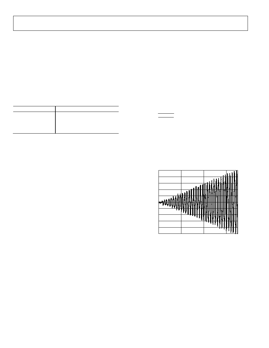
Linear Update Math
Linear math is the addition or subtraction of a constant value
(step). The equation to describe this step size is
(
)
20
10
13
5
2
2
-
◊
=
tconst
step
The result of the equation is normalized to 5.23 data format.
This gives a time constant range from 6.75 ms to 213.4 ms.
(≠60 dB relative to 0 dB full scale). An example of this kind of
update is shown in Figure 13. All slew RAM figure examples,
except the second constant time plot, show a ramp from ≠80 dB
to 0 dB (full scale). All figures except the constant time plots
(Figure 16 and Figure 17) use a time constant of 0x7 (0x0 being
the fastest and 0xF being the slowest).
TIME (ms)
OUTPUT LEVEL (V)
1
0.4
0.6
0.8
0.2
0
≠0.4
≠0.2
≠1
≠0.8
≠0.6
0
10
20
30
04607-0-017
Figure 13. Slew RAM--Linear Update Plot
Constant dB and RC-type (Exponential) Update Math
Exponential math is accomplished by shifts and adds with a
range from 6.1 ms to 1.27 s (≠60 dB relative to 0 dB full scale).
When the ramp type is set to 01 (constant dB), each step size is
set to the current value in the slew data. When the ramp type
bits are set to 10 (RC type), the step sizes are equal to the
difference between the values in the target RAM and slew RAM.
Figure 14 and Figure 15 show examples of this type of
target/slew RAM ramping. A decaying plot of both the
constant dB and RC-type ramps would be a mirror image of
what is shown in Figure 14.

Preliminary Technical Data
AD1941
Rev. PrE | Page 19 of 32
04607-0-018
TIME (ms)
OU
TPU
T
LEVEL (
V
)
1
0.8
0.6
0.4
0.2
0
≠0.6
≠0.4
≠0.2
≠0.8
≠1
0
10
5
20
15
30
25
35
Figure 14. Slew RAM--Constant dB Update Plot
04607-0-019
TIME (ms)
OU
TPU
T
LEVEL (
V
)
1
0.8
0.6
0.4
0.2
0
≠0.6
≠0.4
≠0.2
≠0.8
≠1
0
10
20
30
Figure 15. Slew RAM--RC-Type Update Plot
04607-0-020
TIME (ms)
OU
TPU
T
LEVEL (
V
)
1
0.8
0.6
0.4
0.2
0
≠0.6
≠0.4
≠0.2
≠0.8
≠1
0
10
20
30
Figure 16 Slew RAM--Constant Time Update Plot, Full Scale
04607-0-021
TIME (ms)
OU
TPU
T
LEVEL (
V
)
1
0.8
0.6
0.4
0.2
0
≠0.6
≠0.4
≠0.2
≠0.8
≠1
0
10
20
30
Figure 17 Slew RAM--Constant Time Update Plot, Half Scale
Constant Time Update Math
Constant time math is accomplished by adding a step value that
is calculated after each new target is loaded. The equation for
this step size is
Step
= (Target Data - Slew Data)/(Number of Steps)
Figure 16 shows a plot of the target/slew RAM operating in
constant time mode. For this example, 128 steps are used to
reach the target value. This type of ramping will take a fixed
amount of time for a given number of steps, regardless of the
difference in the initial state and the target value. Figure 17
shows a plot of a constant time ramp from ≠80 dB to ≠6 dB
(half scale) using 128 steps. You can see that the ramp takes the
same amount of time as the previous ramp from ≠80 dB to 0 dB.
SAFELOAD REGISTERS
Many applications require real-time control of signal processing
parameters, such as filter coefficients, mixer gains, multi-
channel virtualizing parameters, or dynamics processing curves.
To prevent instability from occurring, all of the parameters of a
biquad filter must be updated at the same time. Otherwise, the
filter could execute for one or two audio frames with a mix of
old and new coefficients. This mix could cause temporary
instability, leading to transients that could take a long time to
decay. To eliminate this problem, the AD1941 loads a set of
10 registers in the control port (five for 28-bit parameters, and
another five for indirectly addressing the target/slew RAMs)
with the desired parameter or target/slew RAM address and
data. Five registers are used because a biquad filter uses five
coefficients, and it is desirable to be able to do a complete
biquad update in one transaction. The safeload registers can be
used to update either the parameter RAM or target/slew RAM
values. Once these registers are loaded, the appropriate initiate
safe transfer bit (there are separate bits for parameter and
target/slew loads) in the core control register should be set to
initiate the loading into RAM. Program lengths should be
limited to 1,531 cycles (1,536 - 5) to ensure that the SigmaDSP
is able to perform the safeloads. It can be guaranteed that the
safeload will have occurred within one LRCLK period (21 µs at
f
s
= 48 kHz) of the initiate safe transfer bit being set.
The safeload logic automatically sends only those safeload regis-
ters that have been written to since the last safeload operation.
For example, if only two parameters are to be sent, only two of
the five safeload registers must be written to. When the initiate
safe transfer bit (in the core control register) is asserted, only
those two registers are sent; the other three registers are not sent
to the RAM and can still hold old or invalid data.

AD1941
Preliminary Technical Data
Rev. PrE | Page 20 of 32
Table 17. Data Capture Control Registers (2634≠2641)
Register Bits
Function
12:2
11-Bit Program Counter Address
1:0
Register Select
00 = Mult_X_input
01 = Mult_Y_input
10 = MAC_output
11 = Accum_fback
DATA CAPTURE REGISTERS
The AD1941's data capture feature allows the data at any node
in the signal processing flow to be sent to one of six control
port-readable registers or to a serial output pin. This can be
used to monitor and display information about internal signal
levels or compressor/limiter activity.
The AD1941 contains six independent control port-readable
data capture registers, and two digital output capture registers.
The digital output registers are output on SDATA_OUT7 when
the data capture serial out enable bit (Bit 14) is set in Serial
Output Control Register 2. These registers are useful when
debugging the signal processing flow.
For each of the data capture registers, a capture count and a
register select must be set. The capture count is a number
between 0 and 1,535 that corresponds to the program step
number where the capture will occur. The register select field
programs one of four registers in the DSP core that will be
transferred to the data capture register when the program
counter equals the capture count. The register select field
selections are shown in Table 18.
Table 18. Data Capture Output Register Select
Setting Register
00
Multiplier X Input (Mult_X_input)
01
Multiplier Y Input (Mult_Y_input)
10 Multiplier-Accumulator
Output
(MAC_out)
11
Accumulator Feedback (Accum_fback)
The capture count and register select bits are set by writing to
one of the eight data capture registers at register addresses
2634: Control Port Data Capture Setup Register 0
2635: Control Port Data Capture Setup Register 1
2636: Control Port Data Capture Setup Register 2
2637: Control Port Data Capture Setup Register 3
2638: Control Port Data Capture Setup Register 4
2639: Control Port Data Capture Setup Register 5
2640: Digital Out Data Capture Setup Register 0
2641: Digital Out Data Capture Setup Register 1
The captured data is in 5.19 twos complement data format for
all eight register select fields. The four LSBs are truncated from
the internal 5.23 data-word.
The data that must be written to set up the data capture is a
concatenation of the 11-bit program count index with the 2-bit
register select field. The capture count and register select values
that correspond to the desired point to be monitored in the
signal processing flow can be found in a file output from the
program compiler. The capture registers can be accessed by
reading from locations 2634 to 2639 (for control port capture
registers). The format for reading and writing to the data
capture registers can be seen in Table 27 and Table 28.
Table 19. DSP Core Control Register (2642)
Register Bits
Function
15:14
Reserved
13
Slew RAM Muted (Read Only)
12
Mute Slew RAM, All Locations
11
Reserved, Set to 0
10
Use Serial Out LRCLK for Output Latch
9
Clear Internal Registers to All 0s, Active Low
8
Force Multiplier to 0
7
Inititalize Data Memory with 0s
6
Mute Serial Input Port
5
Initiate Safe Transfer to Target RAM
4
Initiate Safe Transfer to Parameter RAM
3:2
Input Serial Port to Sequencer Sync
00 = LRCLK
01 = LRCLK/2
10 = LRCLK/4
11 = LRCLK/8
1:0
Program Length
00 = 1536
01 = 768
10 = 384
11 = 192
DSP CORE CONTROL REGISTER
The controls in this register set the operation of the AD1941's
DSP core. Bits 6 to 9 can be set to initiate a shutdown of the
core. The output is muted when this is performed, so it is best to
first assert the mute slew RAM bit (if slew RAM locations are
used as volume controls in the program) to avoid a click or pop
when shutdown is asserted.
Slew RAM Muted (Bit 13)
This bit is set to 1 when the slew RAM mute operation has been
completed. This bit is read-only and is automatically cleared by
reading.
Mute Slew RAM, All Locations (Bit 12)
Setting this bit to 1 initiates a mute of all 64 slew RAM
locations. When reset to 0, all RAM locations return to their
previous state. This bit is only functional if slew RAM locations
are used in the custom program design. Keep in mind that the
AD1941's default program does not use any slew RAM volume
controls, so this bit has no effect in that case. The mute
operation is identical to writing all 0s to the data portion of the
target RAM, and therefore the time constant and linear/
exponential curve selection is determined by the bits that have
been previously written to the high bits of the target RAM.

Preliminary Technical Data
AD1941
Rev. PrE | Page 21 of 32
Use Serial Out LRCLK for Output Latch (Bit 10)
Normally, data is transferred from the DSP core to the serial
output registers at the end of each program cycle. In some cases
(e.g., when output sample rate is set to some multiple of input
sampling rate), it is desirable to transfer the internal core data
multiple times during a single input audio sample period. Set-
ting this bit to 1 allows the output LRCLK signal to control this
data transfer rather than the internal end-of-sequence signal.
Operation in this mode may require custom assembly-language
coding in the ADI graphical tools.
Clear Registers to All Zeros (Bit 9)
Setting this bit to 0 sets the contents of the accumulators and
serial output registers to 0. Like the other register bits, this one
powers up to 0. This means the AD1941 powers up in clear
mode and will not pass a signal until a 1 is written to this bit.
This is intended to prevent noises from inadvertently occurring
during the power-up sequence.
Force Multiplier to Zero (Bit 8)
When this bit is set to 1, the input to the DSP multiplier is set to
0, which results in the multiplier output being 0. This control bit
is included for maximum flexibility, and is normally not used.
Initialize Data Memory with Zeros (Bit 7)
Setting this bit to 1 initializes all data memory locations to 0.
This bit is cleared to 0 after the operation is complete. This bit
should be asserted after a complete program/parameter
download has occurred to ensure click-free operation.
Zero Serial Input Port (Bit 6)
When this bit is set to 1, the 16 serial input channels are forced
to all 0s.
Initiate Safe Transfer to Target RAM (Bit 5)
Setting this bit to 1 initiates a safeload transfer to the target/slew
RAM. This bit is cleared when the operation is completed.
There are five safeload register pairs (address/data); only those
registers that have been written since the last safeload event are
transferred. Address 0 corresponds to the first target RAM
location.
Initiate Safe Transfer to Parameter RAM (Bit 4)
Setting this bit to 1 initiates a safeload transfer to the parameter
RAM. This bit is cleared when the operation is completed.
There are five safeload registers pairs (address/data); only those
registers that have been written since the last safeload event are
transferred. Address 0 corresponds to the first parameter RAM
location.
Input Serial Port to Sequencer Sync (Bits 3:2)
Normally, the internal sequencer is synchronized to the
incoming audio frame rate by comparing the internal program
counter with the edge of the LRCLK input signal. In some cases
the AD1941 may be used to decimate an incoming signal by
some integer factor. In this case, it is desirable to synchronize
the sequencer to a submultiple of the incoming LRCLK rate so
more than one audio input sample is available to the program
during a single audio output frame. For example, if these bits are
set to 01 (LRCLK/2), a 96 kHz input can be used with a 48 kHz
output, allowing two consecutive input samples to be processed
during a single audio output frame. Operation in this mode
may require custom assembly-language coding in the ADI
graphical tools.
Program Length (Bits 1:0)
96 kHz and 192 kHz Modes
These bits set the length of the internal program. The default
program length is 1,536 instructions for f
s
= 48 kHz, but the
program length can be shortened by factors of 2 to accom-
modate sample rates higher than 48 kHz. For f
s
= 96 kHz the
program length should be set to 768 (01), and the length should
be set at 384 steps (10) for f
s
= 192 kHz. A program length of
192 steps is available, but will not be commonly used.
Low Power Mode
This setting can also be used to reduce the power consumption
of the AD1941. If the program length is set to 768 steps and
f
s
= 48 kHz, instead of 96 kHz, then the power consumption of
the part will be cut in approximately half. Correspondingly,
when the program length is set to 384 steps with f
s
= 48 kHz the
power consumption will be about º of what it is in normal
operation with 1,536 program steps and f
s
= 48 kHz.
Table 20. RAM Configuration Register (2643)
Register Bits
Function
7:4 Reserved
3:0
RAM Modulo, 1 LSB corresponds to
512 locations, max = 0b1100 (6 k)
RAM CONFIGURATION REGISTER
The AD1941 uses a modulo RAM addressing scheme to allow
filters and other blocks to be coded easily without requiring
filter data to be explicitly moved during the filtering operation.
This is accomplished by adding the contents of an address offset
counter to the actual base address supplied in the AD1941's
core. This address offset counter is incremented automatically at
the audio frame rate.
This method works well for most audio applications that
involve filtering. In some cases, however, it is desirable to have
direct access to the RAM, bypassing the autoincrementing
address offset counter. For this reason, the data memory in the
AD1941 can be divided into modulo and nonmodulo portions
by programming the RAM configuration register (Table 20).
The address range from 0 to 512 ◊ (RAM configuration register
contents) is treated as modulo memory with autoincrementing
address offset registers. The maximum setting of this register is
the full size of the RAM, or 6,144 (6 k) data words. Note that
addresses in this range automatically wrap around the modulo
boundary as set by the register. This feature is not normally

AD1941
Preliminary Technical Data
Rev. PrE | Page 22 of 32
used with ADI-supplied blocks. For normal operation, this
register may be left in its default state, which sets up the entire
RAM to use the autoincrement feature. This feature is included
for maximum programming flexibility and may be used in the
case of specialized software development.
CONTROL PORT READ/WRITE DATA FORMATS
The read/write formats of the control port are designed to be
byte-oriented. This allows for easy programming of common
microcontroller chips. In order to fit into a byte-oriented
format, 0s are appended to the data fields before the MSB in
order to extend the data word to the next multiple of eight bits.
For example, 28-bit words written to the parameter RAM are
appended with four leading 0s in order to reach 32 bits
(4 bytes); 40-bit words written to the program RAM are not
appended with any 0s because it is already a full 5 bytes. These
zero-extended data fields are appended to a 3-byte field
consisting of a 7-bit chip address, a read/write bit, and an 11-bit
RAM/register address. The control port knows how many data
bytes to expect based on the address that is received in the first
three bytes.
The total number of bytes for a single-location write command
can vary from four bytes (for a control register write), to eight
bytes (for a program RAM write). Burst mode may be used to
fill contiguous register or RAM locations. A burst mode write is
done by writing the address and data of the first RAM/register
location to be written. Rather than ending the control port
transaction (by bringing the CLATCH signal high in the
AD1941, after the data word, as would be done in a single-
address write, the next data word can be written immediately
without first writing its specific address. The AD1941 control
port auto-increments the address of each write, even across the
boundaries of the different RAMs and registers.
Table 21. Parameter RAM Read/Write Format (Single Address)
Byte 0
Byte 1
Byte 2
Byte 3
Bytes 4≠6
chip_adr [6:0], W/R
0000, param_adr[11:8]
param_adr[7:0]
0000, param[27:24]
param [23:0]
Table 22. Parameter RAM Block Read/Write Format (Burst Mode)
Byte 0
Byte 1
Byte 2
Byte 3
Bytes 4≠6
Byte 7
Byte 11
chip_adr [6:0], W/R
0000, param_adr[11:8]
param_adr[7:0] 0000,
param[27:24] param[23:0] Byte 8
Byte 12
Byte 9
Byte 13
Byte 10
Byte 14
<--param_adr-->
param_adr + 1
param_adr + 2
Table 23. Program RAM Read/Write Format (Single Address)
Byte 0
Byte 1
Byte 2
Bytes 3≠7
chip_adr [6:0], W/R
0000, prog_adr[11:8]
prog_adr[7:0]
prog[39:0]
Table 24. Program RAM Block Read/Write Format (Burst Mode)
Byte 0
Byte 1
Byte 2
Byte 3-7
Byte 8
Byte 13
chip_adr [6:0], W/R
0000, prog_adr[11:8]
prog_adr[7:0]
prog[39:0]
Byte 9
Byte 14
Byte 10
Byte 15
Byte 11
Byte 16
Byte 12
Byte 17
<--prog_adr-->
prog_adr +1
prog_adr +2
Table 25. Control Register Read/Write Format (Core, Serial Out 0, Serial Out 1)
Byte 0
Byte1
Byte 2
Byte 3
Byte 4
chip_adr [6:0], W/R
0000, reg_adr[11:8]
reg_adr[7:0]
data[15:8]
data[7:0]
Table 26. Control Register Read/Write Format (RAM Configuration, Serial Input)
Byte 0
Byte1
Byte 2
Byte 3
chip_adr [6:0], W/R
0000, reg_adr[11:8]
reg_adr[7:0]
data[7:0]

Preliminary Technical Data
AD1941
Rev. PrE | Page 23 of 32
Table 27. Data Capture Register Write Format
Byte 0
Byte 1
Byte 2
Byte 3
Byte 4
chip_adr [6:0], W/R 0000, data_capture_adr[11:8]
data_capture_adr[7:0] 000,
progCount[10:6]
1
progCount[5:0]
1
, regSel[1:0]
2
1
ProgCount[10:0] = value of program counter where trap occurs (the table of values is generated by the program compiler).
2
RegSel[1:0] selects one of four registers (see Data Capture Registers section).
Table 28. Data Capture (Control Port Readback) Register Read Format
Byte 0
Byte 1
Byte 2
Bytes 3≠5
chip_adr [6:0], W/R
0000, data_capture_adr[11:8]
data_capture_adr[7:0]
data[23:0]
Table 29. Safeload Register Data Write Format
Byte 0
Byte 1
Byte 2
Byte 3
Bytes 4≠7
chip_adr [6:0], W/R
0000, safeload_adr[11:8]
safeload_adr[7:0]
000000, data[33:32]
data[31:0]
Table 30. Safeload Register Address Write Format
Byte 0
Byte 1
Byte 2
Byte 3
Byte 4
chip_adr [6:0], W/R
0000, safeload_adr[11:8]
safeload_adr[7:0]
000000, param_adr[9:8]
param_adr[7:0]
AD1941
Preliminary Technical Data
Rev. PrE | Page 24 of 32
SERIAL DATA INPUT/OUTPUT PORTS
The AD1941's flexible serial data input and output ports can be
set to accept or transmit data in 2-channel formats or in an
8- or 16-channel TDM stream. Data is processed in twos
complement, MSB-first format. The left channel data field
always precedes the right channel data field in the 2-channel
streams. In the TDM modes, Slots 0 to 3 (8-channel TDM) or
Slots 0 to 7 (16-channel TDM) fall in the first half of the audio
frame, and Slots 4 to 7 (or Slots 8 to 15 in 16-channel TDM) are
in the second half of the frame. The serial modes are set in the
serial output and serial input control registers.
The input control register allows control of clock polarity and
data input modes. The valid data formats are I
2
S , left-justified,
right-justified (24-, 20-, 18-, or 16-bit), 8-channel, and
16-channel TDM. In all modes except for the right-justified
modes, the serial port will accept an arbitrary number of
bits up to a limit of 24. Extra bits will not cause an error, but
they will be truncated internally. Proper operation of the right-
justified modes requires that there be exactly 64 BCLKs per
audio frame. The TDM data is input on SDATA_IN2 and
SDATA_IN3 when in 2 ◊ 8-channel TDM mode, and on
SDATA_IN2 in 16-channel TDM mode. The LRCLK in TDM
mode can be input to the AD1941 as either a 50/50 duty cycle
clock or as a bit-wide pulse.
The two clock domains on the serial output ports can generate
two separate 8-channel TDM streams or one 16-channel TDM
stream. When in 16-channel TDM mode, the data is clocked by
LRCLK_OUT0 and BCLK_OUT0. The AD1941 must be in
slave mode for 16-channel TDM unless the data is sampled at
48 kHz; the part cannot generate a TDM bit clock that is fast
enough to support 96 kHz or 192 kHz. In 8-channel TDM
mode, the AD1941 can be a master for 48 kHz and 96 kHz data,
but not for 192 kHz data. Table 31 displays the modes in which
the serial output port will function.
The output control registers give the user control of clock
polarities, clock frequencies, clock types, and data format. In all
modes except for the right-justified modes (MSB delayed by 8,
12, or 16), the serial port accepts an arbitrary number of bits up
to a limit of 24. Extra bits will not cause an error, but will be
truncated internally. Proper operation of the right-justified
modes requires the LSB to align with the edge of the LRCLK.
The default settings of all serial port control registers
correspond to 2-channel I
2
S mode. LRCLK_OUT0 and
BCLK_OUT0 are clocks for Serial Output Ports 0 to 7, and
LRCLK_OUT1 and BCLK_OUT1 Clock Ports 8 to 15.
All registers default to being set as all 0s. All register settings
apply to both master and slave modes unless otherwise noted.
Table 32 shows the proper configurations for standard audio
data formats.
Table 31 Serial Output Port Master/Slave Mode Capabilities
f
s
2-Channel Modes (I
2
S, Left-Justified, Right-Justified)
8-Channel TDM
16-Channel TDM
48 kHz
Master and slave
Master and slave
Master and slave
96 kHz
Master and slave
Master and slave
Slave only
192 kHz
Master and slave
Slave only
Slave only
Table 32. Data Format Configurations
Format
LRCLK Polarity
LRCLK Type
BCLK Polarity
MSB Position
I
2
S (Figure 18)
Frame begins on
falling edge
Clock
Data changes on falling edge
Delayed from LRCLK edge by one BCLK
Left-Justified
(Figure 19)
Frame begins on
rising edge
Clock
Data changes on falling edge
Aligned with LRCLK edge
Right-Justified
(Figure 20)
Frame begins on
rising edge
Clock
Data changes on falling edge
Delayed from LRCLK edge by 8, 12, or 16 BCLKs
TDM with Clock
(Figure 21)
Frame begins on
falling edge
Clock
Data changes on falling edge
Delayed from start of word clock by one BCLK
TDM with Pulse
(Figure 22)
Frame begins on
rising edge
Pulse
Data changes on falling edge
Delayed from start of word clock by one BCLK

Preliminary Technical Data
AD1941
Rev. PrE | Page 25 of 32
Table 33. Serial Output Control Register 1
(Channels 0≠7) (2644)
Register Bits
Function
15
Dither Enable
0 = Diabled
1 = Enabled
14
Internally Link TDM Streams into Single,
16-Channel Stream
0 = Indepenent
1 = Linked
13
LRCLK Polarity
0 = Frame Begins on Falling Edge
1 = Frame Begins on Rising Edge
12
BCLK Polarity
0 = Data Changes on Falling Edge
1 = Data Changes on Rising Edge
11
Master/Slave
0 = Slave
1 = Master
10:9
BCLK Frequency (Master Mode only)
00 = core_clock/24
01 = core_clock/12
10 = core_clock/6
11 = core_clock/3
8:7
Frame Sync Frequency (Master Mode only)
00 = core_clock/1536
01 = core_clock/768
10 = core_clock/384
6
Frame Sync Type
0 = LRCLK
1 = Pulse
5
Serial Output/TDM Mode Control
0 = 8 Serial Data Outputs
1 = Enable TDM (8- or 16-Channel) on
SDATA_OUT0
4:2
MSB Position
000 = Delay by 1
001 = Delay by 0
010 = Delay by 8
011 = Delay by 12
100 = Delay by 16
101 Reserved
111 Reserved
1:0
Output Word Length, Channels 0≠7
00 = 24 Bits
01 = 20 Bits
10 = 16 Bits
11 = 16 Bits
Table 34. Serial Output Control Register 2
(Channels 8≠15) (2645)
Register Bits
Function
15
Dither Enable
0 = Disabled
1 = Enabled
14
Data Capture Serial Out Enable
(Uses SDATA_OUT7)
0 = Disable
1 = Enable
13
LRCLK Polarity
0 = Frame Begins on Falling Edge
1 = Frame Begins on Rising Edge
12
BCLK Polarity
0 = Data Changes on Falling Edge
1 = Data Changes on Rising Edge
11
Master/Slave
0 = Slave
1 = Master
10:9
BCLK Frequency (Master Mode only)
00 = core_clock/24
01 = core_clock/12
10 = core_clock/6
11 = core_clock/3
8:7
Frame Sync Frequency (Master Mode only)
00 = core_clock/1536
01 = core_clock/768
10 = core_clock/384
6
Frame Sync Type
0 = LRCLK
1 = Pulse
5
Serial Output/TDM Mode Control
0 = 8 Serial Data Outputs
1 = Enable TDM on SDATA_OUT4 (8-Channel)
or SDATA_OUT0 (16-Channel)
4:2
MSB Position
000 = Delay by 1
001 = Delay by 0
010 = Delay by 8
011 = Delay by 12
100 = Delay by 16
101
Reserved
111 Reserved
1:0
Output Word Length, Channels 8≠15
00 = 24 Bits
01 = 20 Bits
10 = 16 Bits
11 = 16 Bits

AD1941
Preliminary Technical Data
Rev. PrE | Page 26 of 32
SERIAL OUTPUT CONTROL REGISTERS
Dither Enable (Bit 15)
Setting this bit to 1 enables dither on the appropriate channels.
Internally Link TDM Streams into Single 16-Channel Stream
(Bit 14, Serial Output Control Register 1)
When this bit is set to 1, the TDM output stream is output in a
single 16-channel stream on SDATA_OUT0. When set to 0,
TDM data is output on two independent 8-channel streams on
Pins SDATA_OUT0 and SDATA_OUT4.
Data Capture Serial Out Enable (Bit 14, Serial Output
Control Register 2)
When set to 1, SDATA_OUT7 is set as the output of the
data capture digital output registers (2640≠2641). See the
Data Capture Registers section for a full explanation of using
this mode.
LRCLK Polarity (Bit 13)
When set to 0, the left channel data is clocked when LRCLK is
low, and the right data clocked when LRCLK is high. When set
to 1, this is reversed.
BCLK Polarity (Bit 12)
This bit controls on which edge of the bit clock the output data
is clocked. Data changes on the falling edge of BCLK_OUTx
when this bit is set to 0, and on the rising edge when this bit is
set at 1.
Master/Slave (Bit 11)
This bit sets whether the output port is a clock master or slave.
The default setting is slave; on power-up, Pins BCLK_OUTx
and LRCLK_OUTx are set as inputs until this bit is set to 1, at
which time they become clock outputs.
BCLK Frequency (Bits 10:9)
When the output port is being used as a clock master, these bits
set the frequency of the output bit clock, which is divided down
from the internal 73.728 MHz core clock.
Frame Sync Frequency (Bits 8:7)
When the output port is used as a clock master, these bits set the
frequency of the output word clock on the LRCLK_OUTx
pins, which is divided down from the internal 73.728 MHz
core clock.
Frame Sync Type (Bit 6)
This bit sets the type of signal on the LRCLK_OUTx pins.
When set to 0, the signal is a word clock with a 50% duty cycle;
when set to 1, the signal is a pulse with a duration of one bit
clock at the beginning of the data frame.
Serial Output/TDM Mode Control (Bit 5)
Setting this bit to 1 changes the output port from multiple serial
outputs to a single TDM output stream on the appropriate
SDATA_OUTx pin. This bit must be set in both serial output
control registers to enable 16-channel TDM on SDATA_OUT0.
MSB Position (Bits 4:2)
These three bits set the position of the MSB of data with respect
to the LRCLK edge. The data output of the AD1941 is always
MSB first.
Output Word Length (Bits 1:0)
These bits set the word length of the output data-word. All bits
following the LSB are set to 0.
Table 35. Serial Input Control Register (2646)
Register Bits
Function
5
8-/16-channel TDM input
0 = Dual 8-channel TDM
1 = 16-channel TDM input
4
LRCLK polarity
0 = Frame begins on falling edge
1 = Frame begins on rising edge
3
BCLK polarity
0 = Data changes on falling edge
1 = Data changes on rising edge
2:0
Serial Input Mode
000 = I
2
S
001 = Left-justified
010 = TDM
011 = Right-justified, 24-bit
100 = Right-justified, 20-bit
101 = Right-justified, 18-bit
110 = Right-justified, 16-bit
SERIAL INPUT CONTROL REGISTER
8-/16-Channel TDM Input (Bit 5)
Setting this bit to 0 puts the AD1941 into dual 8-channel
TDM input mode, with the two streams coming in on
SDATA_IN2/TDM_IN1 and SDATA_IN3/TDM_IN0.
Channels 0 to 7 will be input on TDM_IN0 and Channels 8
to 15 will come in on TDM_IN1. Setting this bit to 1 puts the
part in 16-channel TDM input mode, input on TDM_IN1.
LRCLK Polarity (Bit 4)
When set to 0, the left channel data on the SDATA_INx pins is
clocked when LRCLK_IN is low; and the right input data
clocked when LRCLK_IN is high. When set to 1, this is
reversed. In TDM mode, when this bit is set to 0, data is clocked
in starting with the next appropriate BCLK edge (set in Bit 3 of
this register) following a falling edge on the LRCLK_IN pin.
When set to 1 and running in TDM mode, the input data is
valid on the BCLK edge following a rising edge on the word
clock (LRCLK_IN). The serial input port can also operate with
a pulse input signal, rather than a clock. In this case, the first
edge of the pulse is used by the AD1941 to start the data frame.
When this polarity bit is set to 0, a low pulse should be used,
and a high pulse should be used when the bit it set to 1.

Preliminary Technical Data
AD1941
Rev. PrE | Page 27 of 32
BCLK Polarity (Bit 3)
This bit controls on which edge of the bit clock the input data
changes, and on which edge it is clocked. Data changes on the
falling edge of BCLK_IN when this bit is set to 0, and on the
rising edge when this bit is set at 1.
Serial Input Mode (Bits 2:0)
These two bits control the data format that the input port
expects to receive. Bits 3 and 4 of this control register will
override the settings in Bits 2:0, so all four bits must be changed
together for proper operation in some modes. The clock
diagrams for these modes are shown in Figure 18, Figure 19,
and Figure 20. Note that for left-justified and right-justified
modes the LRCLK polarity is high, then low, which is opposite
from the default setting of Bit 4.
When these bits are set to accept a TDM input, the AD1941's
data starts after the edge defined by Bit 4. Figure 21 shows an
8-channel TDM stream with a high-to-low triggered LRCLK
and data changing on the falling edge of the BCLK. The
AD1941 expects the MSB of each data slot delayed by one
BCLK from the beginning of the slot, just like in the stereo I
2
S
format. In 8-channel TDM mode, Channels 0 to 3 will be in the
first half of the frame, and Channels 4 to 7 will be in the second
half. When in 16-channel TDM mode, the first half-frame will
hold Channels 0 to 7, and the second half-frame will have
Channels 8 to 15. Figure 22 shows an example of a TDM stream
running with a pulse word clock, which would be used to
interface to ADI codecs in their auxiliary mode. To work in this
mode on either the input or output serial ports, the AD1941
should be set to frame beginning on the rising edge of LRCLK,
data changing on the falling edge of BCLK, and MSB position
delayed from the start of the word clock by one BCLK.
Table 32 explains the clock settings for each of these formats.
LRCLK
BCLK
SDATA
MSB
LEFT CHANNEL
LSB
MSB
RIGHT CHANNEL
LSB
1 /F
S
04607-0-023
Figure 18. I
2
S Mode--16 to 24 Bits per Channel
LRCLK
BCLK
SDATA
LEFT CHANNEL
MSB
LSB
MSB
RIGHT CHANNEL
LSB
1 /F
S
04607-0-024
Figure 19. Left-Justified Mode--16 to 24 Bits per Channel
LRCLK
BCLK
SDATA
LEFT CHANNEL
MSB
LSB
MSB
RIGHT CHANNEL
LSB
1 /F
S
04607-0-025
Figure 20. Right-Justified Mode--16 to 24 Bits per Channel

AD1941
Preliminary Technical Data
Rev. PrE | Page 28 of 32
LRCLK
BCLK
DATA
SLOT 1
SLOT 2
SLOT 5
SLOT 6
32 BCLKs
MSB
MSB≠1
MSB≠2
256 BCLKs
SLOT 3
SLOT 4
SLOT 7
SLOT 8
LRCLK
BCLK
DATA
04607-0-012
Figure 21. 8-Channel TDM Mode. This diagram shows just one of the formats in which the AD1941 can operate in TDM mode. Please refer to the Serial Data
Input/Output Ports section for a more complete description of the modes of operation.
LRCLK
SLOT 0
SLOT 1
SLOT 2
SLOT 3
SLOT 4
SLOT 5
SLOT 6
SLOT 7
CH
0
BCLK
SDATA
MSB TDM
8TH
CH
32
BCLKs
MSB TDM
04607-0-022
Figure 22. TDM Mode with Pulse Word Clock
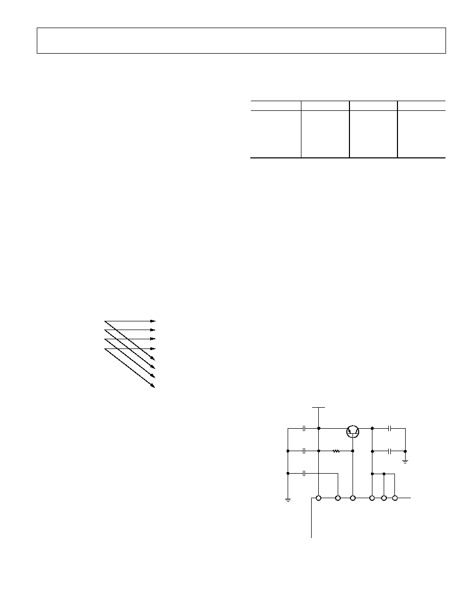
Preliminary Technical Data
AD1941
Rev. PrE | Page 29 of 32
INITIALIZATION
POWER-UP SEQUENCE
The AD1941 has a built-in power-up sequence that initializes
the contents of all internal RAMs. During this time, the
contents of the internal program boot ROM are copied to the
internal program RAM memory, and the parameter RAM
(all 0s) is filled with values from its associated boot ROM. The
default boot ROM program simply copies the serial inputs to
the serial outputs with no processing. The data memories are
also cleared during this time.
The boot sequence, which starts on the rising edge of the
RESETB pin, lasts for 8,192 cycles of the signal on the MCLK
pin at start-up. Assuming even the slowest possible signal on
this pin, a 64 ◊ f
S
clock, the boot sequence will still complete
before the PLL locks to the input clock. Since the boot sequence
requires a stable master clock, the user should avoid writing to
or reading from the registers until the MCLK input signal has
settled and the PLL has locked. The PLL takes approximately
3 ms to lock. Coming out of reset, the clock mode is imme-
diately set by the PLL_CTRL0, PLL_CTRL1, and PLL_CTRL2
pins. Reset is synched to the falling edge of the internal MCLK.
The power-up default signal processing flow in the AD1941
simply takes the eight inputs and copies these signals to the
16 digital outputs, as shown in Figure 23.
04607-0-004
SDATA_IN0
SDATA_IN1
SDATA_IN2
SDATA_IN3
SDATA_OUT0
SDATA_OUT1
SDATA_OUT2
SDATA_OUT3
SDATA_OUT4
SDATA_OUT5
SDATA_OUT6
SDATA_OUT7
Figure 23. Default Program Signal Flow
SETTING MASTER CLOCK/PLL MODE
The AD1941's MCLK input feeds a PLL, which generates the
1536 ◊ f
S
clock to run the DSP core. In normal operation, the
input to MCLK must be one of the following; 64 ◊ f
S
, 256 ◊ f
S
,
384 ◊ f
S
, or 512 ◊ f
S
, where f
S
is the input sampling rate. The
mode is set on PLL_CTRL0, PLL_CTRL1, and PLL_CTRL2,
according to Table 36. If the AD1941 is set to receive double-
rate signals (by reducing the number of program steps/sample
by a factor of 2 using the core control register), then the master
clock frequencies must be either 32 ◊ f
S
, 128 ◊ f
S
, 192 ◊ f
S
, or
256 ◊ f
S
. If the AD1941 is set to receive quad-rate signals (by
reducing the number of program steps/sample by a factor of 4
using the core control register), then the master clock
frequencies must be one of 16 ◊ f
S
, 64 ◊ f
S
, 96 ◊ f
S
, or 128 ◊ f
S
.
On power-up, a clock signal must be present on MCLK so that
the AD1941 can complete its initialization routine. The PLL can
also run in bypass mode, where the clock present on MCLK is
fed directly to the DSP core, although this setting is not
recommended for normal operation.
Table 36. PLL Modes
MCLK
Input PLL_CTRL2 PLL_CTRL1 PLL_CTRL0
64 ◊ f
S
0 0 0
256 ◊ f
S
0 1 0
384 ◊ f
S
X
1
X
1
1
512 ◊ f
S
1 0 0
Bypass
1 1 0
1
X = don't care
The clock mode should not be changed without also resetting
the AD1941. If the mode is changed on the fly, a click or pop
may result on the outputs. The state of the PLL_CTRLx pins
should be changed while RESETB is held low.
VOLTAGE REGULATOR
The AD1941 includes an on-board voltage regulator that allows
the chip to be used in systems where a 2.5 V supply is not
available, but 3.3 V or 5 V is. The only external components
needed for this are a PNP transistor such as an FZT953, a single
capacitor, and a single resistor. The recommended design for the
voltage regulator is shown in Figure 24. The 10 µF and 100 nF
capacitors shown in this schematic are recommended for
bypassing, but are not necessary for operation. Here, VDD is the
main system voltage (3.3 V or 5 V) and should be connected to
VSUPPLY. 2.5 V is generated at the transistor's collector, which
is connected to the VDD pins, PLL_VDD and VSENSE. The
reference voltage on VREF is 1.15 V and is generated by the
regulator. A 1 nF capacitor should be connected between this
pin and ground. VDRIVE is connected to the base of the PNP
transistor. A 1 k resistor should be connected between
VDRIVE and VSUPPLY.
If the regulator is not used in the design, VSUPPLY, VREF,
VDRIVE, and VSENSE can be tied to ground.
10
µ
F
10
µ
F
100nF
100nF
1nF
1k
AD1940
DVDD
FZT953
04607-0-009
VSU
PPLY
VR
EF
V
DRIV
E
VSEN
SE
VD
D
+
+
PLL_VDD
Figure 24. Voltage Regulator Design

AD1941
Preliminary Technical Data
Rev. PrE | Page 30 of 32
OUTLINE DIMENSIONS
TOP VIEW
(PINS DOWN)
1
12
13
25
24
36
37
48
0.27
0.22
0.17
0.50
BSC
7.00
BSC SQ
SEATING
PLANE
1.60
MAX
0.75
0.60
0.45
VIEW A
9.00 BSC
SQ
PIN 1
0.20
0.09
1.45
1.40
1.35
0.08 MAX
COPLANARITY
VIEW A
ROTATED 90
∞
CCW
SEATING
PLANE
10∞
6∞
2∞
7∞
3.5∞
0∞
0.15
0.05
COMPLIANT TO JEDEC STANDARDS MS-026BBC
Figure 25. 48-Lead Low-Profile Quad Flat Package [LQFP]
Dimensions Shown in Millimeters
ORDERING GUIDE
Model
Temperature Range
Package Description
Package Option
AD1941YSTZ
1
≠40∞C to +105∞C
48-Lead LQFP
ST-48
AD1941YSTZRL
1
≠40∞C to +105∞C
48-Lead LQFP
ST-48 in 13" Reel
1
Z= Pb-free part.

Preliminary Technical Data
AD1941
Rev. PrE | Page 31 of 32
NOTES

AD1941
Preliminary Technical Data
Rev. PrE | Page 32 of 32
NOTES
© 2005 Analog Devices, Inc. All rights reserved. Trademarks and registered
trademarks are the property of their respective owners.
C0
4607-0-2/05(PrE)