Document Outline
- FEATURES
- APPLICATIONS
- PRODUCT OVERVIEW
- FUNCTIONAL BLOCK DIAGRAM
- TABLE OF CONTENTS
- SPECIFICATIONS
- TEST CONDITIONS, UNLESS OTHERWISE NOTED.
- ANALOG PERFORMANCE
- DIGITAL I/O
- POWER
- TEMPERATURE RANGE
- DIGITAL TIMING
- DIGITAL FILTER CHARACTERISTICS at 44.1 kHz
- ABSOLUTE MAXIMUM RATINGS
- ORDERING GUIDE
- PIN CONFIGURATION
- PIN FUNCTION DESCRIPTIONS
- Typical Performance Characteristics
- PRODUCT OVERVIEW
- Features
- Pin Functions
- SDATA0, 1, 2ÑSerial Data Inputs.
- LRCLK0, 1, 2ÑLeft/Right Clocks for Framing the Input Data.
- BCLK0, 1, 2ÑSerial Bit Clocks for Clocking in the Serial Data.
- DMUXO/TDMO, LRMUXO/TDMFS, BMUXO/TDMBC
- MCLK0, 1, 2ÑMaster Clock Inputs.
- MCLKOÑMaster Clock Output.
- CDATAÑSerial Data In for the SPI Control Port.
- COUTÑSerial Data Output.
- CCLKÑSPI Bit Rate Clock.
- CLATCHÑSPI Latch Signal.
- RESETBÑActive-Low Reset Signal.
- ZEROFLAGÑZero-Input Indicator.
- DCSOUTÑData Capture Serial Out.
- AUXDATAÑAuxiliary Serial Data Input.
- MUTEÑMute Output Signal.
- VOUTL+, VOUTLÖ ÑLeft-Channel Differential Analog Outputs.
- VOUTR+, VOUTRÖ ÑRight Channel Differential Outputs.
- VOUTS+, VOUTSÖ ÑSub Channel Differential Outputs.
- VREFÑAnalog Reference Voltage Input.
- FILTCAPÑFilter Capacitor Point.
- DVDDÑDigital VDD for Core.
- ODVDDÑDigital VDD for All Digital Outputs.
- DGND (2)ÑDigital Ground.
- AVDD (3)ÑAnalog VDD.
- AGND (3)ÑAnalog Ground.
- SIGNAL PROCESSING
- Signal Processing Overview
- Numeric Formats
- Coefficient Format
- Internal DSP Signal Data Format
- High-Pass Filter
- Biquad Filters
- Volume
- Stereo Image Expander
- Delay
- Main Compressor/Limiter
- RMS Time Constant
- RMS Hold Time
- RMS Release Rate
- Look-Ahead Delay
- Post-Compression Gain
- Subwoofer Compressor/Limiter
- De-emphasis Filtering
- Using the Sub Reinjection Paths for Systems with No Subwoofer
- Interpolation Filters
- SPI PORT
- Overview
- SPI Address Decoding
- Control Register 1
- Control Register 2
- Volume Registers
- Parameter RAM Contents
- Options for Parameter Updates
- Soft Shutdown Mechanism
- Safeload Mechanism
- Summary of RAM Modes
- SPI READ/WRITE DATA FORMATS
- INITIALIZATION
- Power-Up Sequence
- Setting the Clock Mode
- Setting the Data and MCLK Input Selectors
- DATA CAPTURE REGISTERS AND OUTPUTS
- SERIAL DATA INPUT/OUTPUT PORTS
- Serial Data Input/Output Modes
- DIGITAL CONTROL PIN
- ANALOG OUTPUT SECTION
- GRAPHICAL CUSTOM PROGRAMMING TOOLS
- APPENDIX
- OUTLINE DIMENSIONS
REV. 0
a
AD1953
Information furnished by Analog Devices is believed to be accurate and
reliable. However, no responsibility is assumed by Analog Devices for its
use, nor for any infringements of patents or other rights of third parties that
may result from its use. No license is granted by implication or otherwise
under any patent or patent rights of Analog Devices. Trademarks and
registered trademarks are the property of their respective companies.
One Technology Way, P.O. Box 9106, Norwood, MA 02062-9106, U.S.A.
Tel: 781/329-4700
www.analog.com
Fax: 781/326-8703
© 2003 Analog Devices, Inc. All rights reserved.
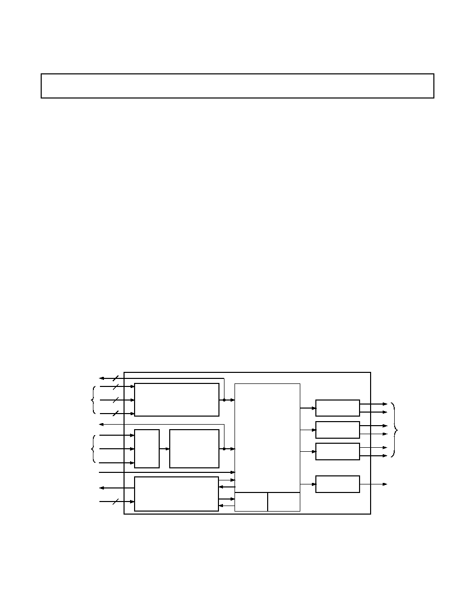
FUNCTIONAL BLOCK DIAGRAM
SERIAL CONTROL
INTERFACE
MCLK
MUX
MCLK
GENERATOR
(256/512 f
S
)
DAC ≠ L
DAC ≠ R
DAC ≠ SW
DATA CAPTURE
OUT/TDM OUT
AUDIO DATA
MUX
26 22
DSP CORE
DATA FORMAT:
3.23 (SINGLE PRECISION)
3.45 (DOUBLE PRECISION)
RAM
ROM
3
3
3
3
3
ANALOG
OUTPUTS
AD1953
MASTER CLOCK
OUTPUT
SERIAL DATA
INPUTS
MASTER
CLOCK INPUTS
SERIAL DATA
OUTPUT
SPI INPUT
SPI DATA
OUTPUT
AUX SERIAL
DATA INPUT
DIGITAL
OUTPUT
SigmaDSP
TM
3-Channel, 26-Bit
Signal Processing DAC
FEATURES
5 V 3-Channel Audio DAC System
Digital Audio Output (2-Channel or 6-Channel
Packed Mode)
Accepts Sample Rates up to 48 kHz
7 Biquad Filter Sections per Channel
Dual Dynamic Processor with Arbitrary Input/Output
Curve and Adjustable Time Constants
0 ms to 6 ms Variable Delay/Channel for Speaker Alignment
Stereo Spreading Algorithm for Phat StereoTM Effect
Program RAM Allows Complete New Program Download
via SPI Port
Parameter RAM Allows Complete Control of More Than
200 Parameters via SPI Port
SPI Port Features Safe-Upload Mode for Transparent
Filter Updates
2 Control Registers Allow Complete Control of Modes
and Memory Transfers
Differential Output for Optimum Performance
112 dB Signal-to-Noise (Not Muted) at 48 kHz Sample
Rate (A-Weighted Stereo)
70 dB Stop-Band Attenuation
On-Chip Clickless Volume Control
Hardware and Software Controllable Clickless Mute
Digital De-emphasis Processing for 32 kHz, 44.1 kHz, 48 kHz
Sample Rates
Flexible Serial Data Port with Right-Justified, Left-Justified,
I
2
S Compatible, and DSP Serial Port Modes
Auxiliary Digital Input
Graphical Custom Programming Tools
48-Lead LQFP Plastic Package
APPLICATIONS
2.0/2.1 Channel Audio Systems (2 Main Channels
Plus Subwoofer)
Multichannel Automotive Sound Systems
Multimedia Audio
Mini Component Stereo
Home Theater Systems (AC-3 Postprocessor)
Musical Instruments
In-Seat Sound Systems (Aircraft, Motor Coaches)
PRODUCT OVERVIEW
The AD1953 is a complete 26-bit, single-chip, 3-channel digital
audio playback system with built-in DSP functionality for speaker
equalization, dual-band compression/limiting, delay compensa-
tion, and image enhancement. These algorithms can be used to
compensate for real-world limitations of speakers, amplifiers,
and listening environments, resulting in a dramatic improvement
of perceived audio quality.
The signal processing used in the AD1953 is comparable to that
found in high end studio equipment. Most of the processing is
done in full 48-bit double-precision mode, resulting in very good
low level signal performance and the absence of limit cycles or
idle tones. The compressor/limiter uses a sophisticated two-band
algorithm often found in high end broadcast compressors.
(continued on page 9)

REV. 0
AD1953
≠2≠
TABLE OF CONTENTS
FEATURES . . . . . . . . . . . . . . . . . . . . . . . . . . . . . . . . . . . . . 1
APPLICATIONS . . . . . . . . . . . . . . . . . . . . . . . . . . . . . . . . . 1
PRODUCT OVERVIEW . . . . . . . . . . . . . . . . . . . . . . . . . . . 1
FUNCTIONAL BLOCK DIAGRAM . . . . . . . . . . . . . . . . . 1
SPECIFICATIONS . . . . . . . . . . . . . . . . . . . . . . . . . . . . . . . 3
ABSOLUTE MAXIMUM RATINGS . . . . . . . . . . . . . . . . . 6
ORDERING GUIDE . . . . . . . . . . . . . . . . . . . . . . . . . . . . . . 6
Package Characteristics . . . . . . . . . . . . . . . . . . . . . . . . . . . 6
PIN CONFIGURATION . . . . . . . . . . . . . . . . . . . . . . . . . . . 6
PIN FUNCTION DESCRIPTIONS . . . . . . . . . . . . . . . . . . 7
TYPICAL PERFORMANCE CHARACTERISTICS . . . . . 8
PERFORMANCE PLOTS . . . . . . . . . . . . . . . . . . . . . . . . . . 8
PRODUCT OVERVIEW . . . . . . . . . . . . . . . . . . . . . . . . . . . 9
Features . . . . . . . . . . . . . . . . . . . . . . . . . . . . . . . . . . . . . . . 9
Pin Functions . . . . . . . . . . . . . . . . . . . . . . . . . . . . . . . . . 10
SIGNAL PROCESSING . . . . . . . . . . . . . . . . . . . . . . . . . . 12
Signal Processing Overview . . . . . . . . . . . . . . . . . . . . . . . 12
Numeric Formats . . . . . . . . . . . . . . . . . . . . . . . . . . . . . . 13
Coefficient Format . . . . . . . . . . . . . . . . . . . . . . . . . . . . . 13
Internal DSP Signal Data Format . . . . . . . . . . . . . . . . . . 13
High-Pass Filter . . . . . . . . . . . . . . . . . . . . . . . . . . . . . . . . 13
Biquad Filters . . . . . . . . . . . . . . . . . . . . . . . . . . . . . . . . . 13
Volume . . . . . . . . . . . . . . . . . . . . . . . . . . . . . . . . . . . . . . 14
Stereo Image Expander . . . . . . . . . . . . . . . . . . . . . . . . . . 14
Delay . . . . . . . . . . . . . . . . . . . . . . . . . . . . . . . . . . . . . . . . 15
Main Compressor/Limiter . . . . . . . . . . . . . . . . . . . . . . . . 15
RMS Time Constant . . . . . . . . . . . . . . . . . . . . . . . . . . . . 17
RMS Hold Time . . . . . . . . . . . . . . . . . . . . . . . . . . . . . . . 17
RMS Release Rate . . . . . . . . . . . . . . . . . . . . . . . . . . . . . . 17
Look-Ahead Delay . . . . . . . . . . . . . . . . . . . . . . . . . . . . . . 17
Post-Compression Gain . . . . . . . . . . . . . . . . . . . . . . . . . . 17
Subwoofer Compressor/Limiter . . . . . . . . . . . . . . . . . . . . 17
De-Emphasis Filtering . . . . . . . . . . . . . . . . . . . . . . . . . . . 18
Using the Sub Reinjection Paths for Systems with No
Subwoofer . . . . . . . . . . . . . . . . . . . . . . . . . . . . . . . . . . . . 18
Interpolation Filters . . . . . . . . . . . . . . . . . . . . . . . . . . . . . 18
SPI PORT . . . . . . . . . . . . . . . . . . . . . . . . . . . . . . . . . . . . . . 18
Overview . . . . . . . . . . . . . . . . . . . . . . . . . . . . . . . . . . . . . 18
SPI Address Decoding . . . . . . . . . . . . . . . . . . . . . . . . . . . 19
Control Register 1 . . . . . . . . . . . . . . . . . . . . . . . . . . . . . . 21
Control Register 2 . . . . . . . . . . . . . . . . . . . . . . . . . . . . . . 22
Volume Registers . . . . . . . . . . . . . . . . . . . . . . . . . . . . . . . 23
Parameter RAM Contents . . . . . . . . . . . . . . . . . . . . . . . . 23
Options for Parameter Updates . . . . . . . . . . . . . . . . . . . . 24
Soft Shutdown Mechanism . . . . . . . . . . . . . . . . . . . . . . . 25
Safeload Mechanism . . . . . . . . . . . . . . . . . . . . . . . . . . . . 25
Summary of RAM Modes . . . . . . . . . . . . . . . . . . . . . . . . 25
SPI READ/WRITE DATA FORMATS . . . . . . . . . . . . . . . 26
INITIALIZATION . . . . . . . . . . . . . . . . . . . . . . . . . . . . . . . 27
Power-Up Sequence . . . . . . . . . . . . . . . . . . . . . . . . . . . . 27
Setting the Clock Mode . . . . . . . . . . . . . . . . . . . . . . . . . . 27
Setting the Data and MCLK Input Selectors . . . . . . . . . . 28
DATA CAPTURE REGISTERS AND OUTPUTS . . . . . . 28
SERIAL DATA INPUT/OUTPUT PORTS . . . . . . . . . . . . 30
Serial Data Input/Output Modes . . . . . . . . . . . . . . . . . . . 30
DIGITAL CONTROL PIN . . . . . . . . . . . . . . . . . . . . . . . . 31
Mute . . . . . . . . . . . . . . . . . . . . . . . . . . . . . . . . . . . . . . . . 31
ANALOG OUTPUT SECTION . . . . . . . . . . . . . . . . . . . . 31
GRAPHICAL CUSTOM PROGRAMMING TOOLS . . . . 32
APPENDIX . . . . . . . . . . . . . . . . . . . . . . . . . . . . . . . . . . . . . 33
OUTLINE DIMENSIONS . . . . . . . . . . . . . . . . . . . . . . . . . 34

≠3≠
REV. 0
TEST CONDITIONS, UNLESS OTHERWISE NOTED.
Supply Voltages (AVDD, DVDD)
5.0 V
Ambient Temperature
25
∞C
Input Clock
12.288 MHz
Input Signal
1.000 kHz 0 dB Full Scale
Input Sample Rate
48 kHz
Measurement Bandwidth
20 Hz to 20 kHz
Word Width
24 Bits
Load Capacitance
2200 pF
Load Impedance
2.74 k
Input Voltage High
2.1 V
Input Voltage Low
0.8 V
ANALOG PERFORMANCE*
Parameter
Min
Typ
Max
Unit
RESOLUTION
24
Bits
SIGNAL-TO-NOISE RATIO (20 Hz to 20 kHz) (Left/Right Output)
No Filter (Stereo)
109
dB
With A-Weighted Filter
112
dB
DYNAMIC RANGE (20 Hz to 20 kHz, ≠60 dB Input) (Left/Right Output)
No Filter
109
dB
With A-Weighted Filter
108
112
dB
TOTAL HARMONIC DISTORTION PLUS NOISE (Left/Right Output)
V
O
= ≠0.5 dB
≠93
≠100
dB
SIGNAL-TO-NOISE RATIO (20 Hz to 20 kHz) (Subwoofer Output)
No Filter (Stereo)
104
dB
With A-Weighted Filter
107
dB
DYNAMIC RANGE (20 Hz to 20 kHz, ≠60 dB Input) (Subwoofer Output)
No Filter
104
dB
With A-Weighted Filter
104
107
dB
TOTAL HARMONIC DISTORTION PLUS NOISE (Subwoofer Output)
V
O
= ≠0.5 dB
≠90
≠96
dB
ANALOG OUTPUTS
Differential Output Range (
± Full Scale) (Left/Right Output)
2.72
V p-p
Differential Output Range (
± Full Scale) (Subwoofer Output)
2.79
V p-p
CMOUT
2.50
V
DC ACCURACY
Gain Error (Left/Right Channel)
≠5
+5
%
Gain Error (Subwoofer Channel)
≠8
+8
%
Interchannel Gain Mismatch
≠0.250
+0.250
dB
Gain Drift
150
ppm/
∞C
DC Offset
≠35
+35
mV
INTERCHANNEL CROSSTALK (EIAJ Method)
≠120
dB
INTERCHANNEL PHASE DEVIATION
±0.1
Degrees
MUTE ATTENUATION
≠107
dB
DE-EMPHASIS GAIN ERROR
±0.1
dB
*Performance of right and left channels is identical (exclusive of the Interchannel Gain Mismatch and Interchannel Phase Deviation specifications).
Specifications subject to change without notice.
SPECIFICATIONS
AD1953

REV. 0
AD1953
≠4≠
DIGITAL I/O
Parameter
Min
Typ
Max
Unit
Input Voltage High (V
IH
)
2.1
V
Input Voltage High (V
IH
) ≠ RESETB
2.25
V
Input Voltage Low (V
IL
)
0.8
V
Input Leakage (I
IH
@ V
IH
= 2.1 V)
10
µA
Input Leakage (I
IL
@ V
IL
= 0.8 V)
10
µA
High Level Output Voltage (V
OH
), I
OH
= 2 mA
DVDD ≠ 0.5
V
Low Level Output Voltage (V
OL
), I
OL
= 2 mA
0.4
V
Input Capacitance
20
pF
Specifications subject to change without notice.
POWER
Parameter
Min
Typ
Max
Unit
SUPPLIES
*
Voltage: Analog, and Digital
4.5
5
5.5
V
Analog Current
42
48
mA
Analog Current, Power-Down
40
46
mA
Digital Current
66
76
mA
Digital Current, SPI Power-Down
6
10
mA
Digital Current, Reset Power-Down
54
62
mA
DISSIPATION
Operation, Both Supplies
540
mW
Operation, Analog Supplies
210
mW
Operation, Digital Supplies
330
mW
SPI Power-Down, Both Supplies
230
mW
Reset Power-Down, Both Supplies
470
mW
POWER SUPPLY REJECTION RATIO
1 kHz 300 mV p-p Signal at Analog Supply Pins
≠80
dB
20 kHz 300 mV p-p Signal at Analog Supply Pins
≠80
dB
*ODVDD current is dependent on load capacitance and clock rate.
Specifications subject to change without notice.
TEMPERATURE RANGE
Parameter
Min
Typ
Max
Unit
Specifications Guaranteed
25
∞C
Functionality Guaranteed
≠40
105
∞C
Storage
≠55
125
∞C
Specifications subject to change without notice.

REV. 0
≠5≠
AD1953
DIGITAL TIMING
Parameter
Min
Typ
Max
Unit
t
DMD
MCLK Recommended Duty Cycle @ 12.288 MHz (256 f
S
Mode)
45
55
%
t
DMD
MCLK Recommended Duty Cycle @ 24.576 MHz (512 f
S
Mode)
40
60
%
t
DMD
MCLK Delay (All Mode)
25
ns
t
DBH
BCLK Low Pulsewidth
10
ns
t
DBH
BCLK High Pulsewidth
10
ns
t
DBD
BCLK Delay (to BCLKO)
25
ns
t
DLS
LRCLK Setup
0
ns
t
DLH
LRCLK Hold
10
ns
t
DLD
LRCLK Delay (to LRCLKO)
25
ns
t
DDS
SDATA Setup
0
ns
t
DDH
SDATA Hold
10
ns
t
DDD
SDATA Delay (to SDATAO)
25
ns
t
TFS
TDMFS Delay (from MCLK)
35
ns
t
TBS
TDMBC Delay (from MCLK)
35
ns
t
TOS
TDMO Delay (from TDMBC)
5
ns
t
CCL
CCLK Low Pulsewidth
12
ns
t
CCH
CCLK High Pulsewidth
12
ns
t
CLS
CLATCH Setup
10
ns
t
CLH
CLATCH Hold
10
ns
t
CLD
CLATCH High Pulsewidth
10
ns
t
CDS
CDATA Setup
0
ns
t
CDH
CDATA Hold
10
ns
t
COD
COUT Delay
35
ns
t
COH
COUT Hold
2
ns
t
DCD
DCSOUT Delay
35
ns
t
DCH
DCSOUT Hold
2
ns
t
PDRP
PD/RST Low Pulsewidth
5
ns
Specifications subject to change without notice.
DIGITAL FILTER CHARACTERISTICS at 44.1 kHz
Parameter
Min
Typ
Max
Unit
Pass-Band Ripple
±0.01
dB
Stop-Band Attenuation
70
dB
Pass Band
20
kHz
0.4535 f
S
Stop Band
24
kHz
0.5442 f
S
Group Delay
24.625/f
S
sec
Specifications subject to change without notice.
REV. 0
AD1953
≠6≠
ABSOLUTE MAXIMUM RATINGS
*
DVDD to DGND . . . . . . . . . . . . . . . . . . . . . . ≠0.3 V to +6 V
ODVDD to DGND . . . . . . . . . . . . . . . . . . . . . ≠0.3 V to +6 V
AVDD to AGND . . . . . . . . . . . . . . . . . . . . . . ≠0.3 V to +6 V
Digital Inputs . . . . . . . . . . DGND ≠ 0.3 V to DVDD + 0.3 V
Analog Inputs . . . . . . . . . . AGND ≠ 0.3 V to AVDD + 0.3 V
AGND to DGND . . . . . . . . . . . . . . . . . . . . ≠0.3 V to +0.3 V
Reference Voltage . . . . . . . . . . . . . . . . . . . (AVDD + 0.3)/2 V
Maximum Junction Temperature . . . . . . . . . . . . . . . . 125
C
Storage Temperature Range . . . . . . . . . . . . ≠65
C to +150C
Soldering . . . . . . . . . . . . . . . . . . . . . . . . . . . . . . 300
C/10 sec
*Stresses above those listed under Absolute Maximum Ratings may cause perma-
nent damage to the device. This is a stress rating only; functional operation of the
device at these or any other conditions above those indicated in the operational
section of this specification is not implied. Exposure to absolute maximum rating
conditions for extended periods may affect device reliability.
Package Characteristics (48-Lead LQFP)
Min
Typ
Max
Unit
JA
(Thermal Resistance
76
C/W
[Junction-to-Ambient])
JC
(Thermal Resistance
17
C/W
[Junction-to-Case])
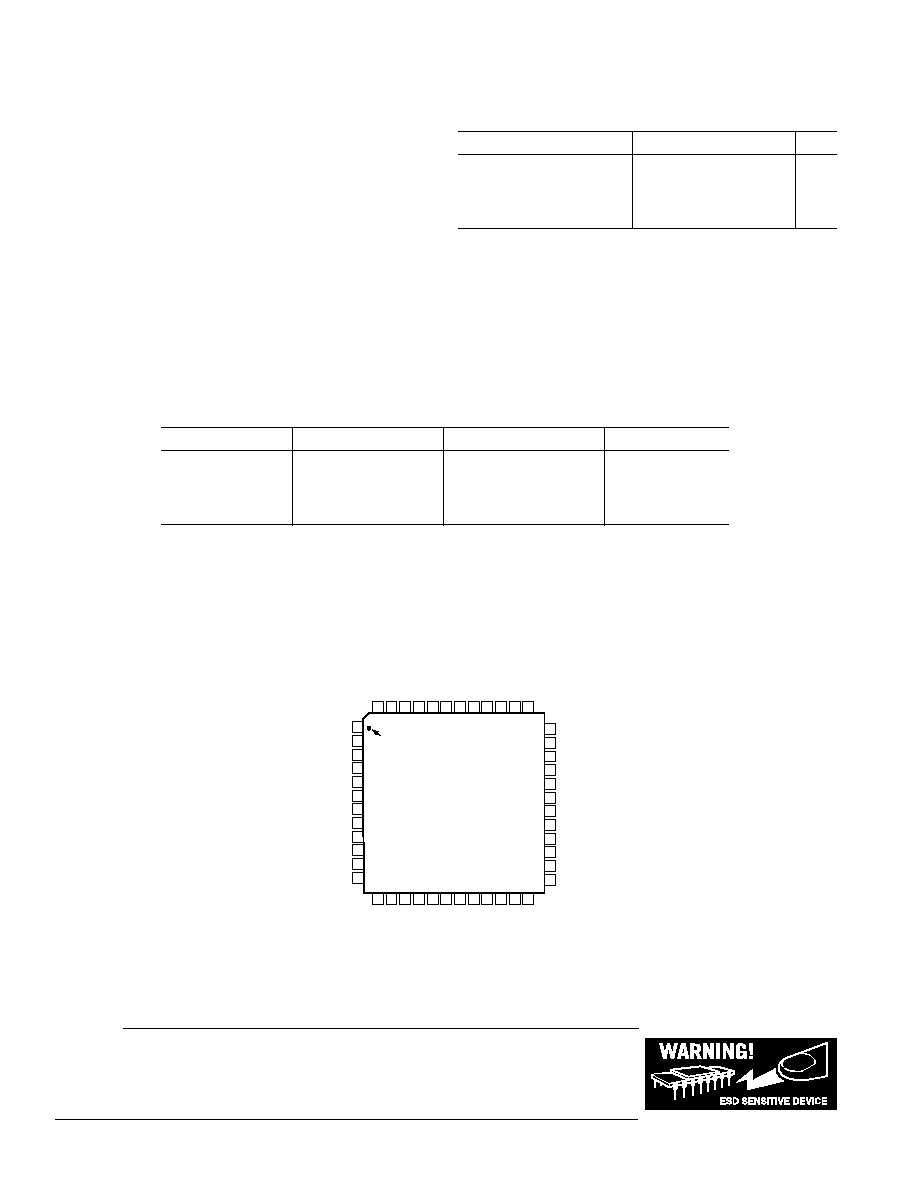
PIN CONFIGURATION
48-Lead LQFP
36
35
34
33
32
31
30
29
28
27
26
25
13 14 15 16 17 18 19 20 21 22 23 24
1
2
3
4
5
6
7
8
9
10
11
12
48 47 46 45 44
39 38 37
43 42 41 40
PIN 1
IDENTIFIER
TOP VIEW
(Not to Scale)
NC
AGND
VOUTL≠
VOUTL+
AVDD
AGND
AVDD
NC
MCLK2
MCLK1
MCLK0
AUXDATA
MUTE
DVDD
NC = NO CONNECT
SDATA2
BCLK2
LRCLK2
SDATA1
VOUTR+
VOUTR≠
AGND
VOUTS+
AD1953
BCLK1
VOUTS≠
DGND
MCLK
OUT
COUT
DCSOUT
OD
VDD
LRMUXO/TDMFS
BMUXO/TDMBC
DMUXO/TDMO
ZER
OFLA
G
FIL
TCAP
VREF
NC
DGND
LRCLK1
SD
A
T
A0
BCLK0
LRCLK0
CD
A
T
A
CCLK
CLA
TCH
RESETB
AV
D
D
A
GND
NC
CAUTION
ESD (electrostatic discharge) sensitive device. Electrostatic charges as high as 4000 V readily
accumulate on the human body and test equipment and can discharge without detection. Although
the AD1953 features proprietary ESD protection circuitry, permanent damage may occur on
devices subjected to high energy electrostatic discharges. Therefore, proper ESD precautions are
recommended to avoid performance degradation or loss of functionality.
ORDERING GUIDE
Model
Temperature Range
Package Description
Package Option
AD1953YST
≠40
C to +105C
48-Lead LQFP
ST-48
AD1953YSTRL
≠40
C to +105C
48-Lead LQFP
ST-48 on 13" Reel
AD1953YSTRL7
≠40
C to +105C
48-Lead LQFP
ST-48 on 7" Reel
EVAL-AD1953EB
Evaluation Board

REV. 0
AD1953
≠7≠
PIN FUNCTION DESCRIPTIONS
Input/
Pin No.
Mnemonic
Output
Description
1
NC
No Connect
2
MCLK2
IN
Master Clock Input 2 256/512 f
S
3
MCLK1
IN
Master Clock Input 1 256/512 f
S
4
MCLK0
IN
Master Clock Input 0 256/512 f
S
5
AUXDATA
IN
Auxiliary Serial Data Input
6
MUTE
IN
Mute Signal, Initiates Volume Ramp-Down
7
DVDD
Digital Supply for DSP Core, 4.5 V to 5.5 V
8
SDATA2
IN
Serial Data Input 2
9
BCLK2
IN
Bit Clock 2
10
LRCLK2
IN
Left/Right Clock 2
11
SDATA1
IN
Serial Data Input 1
12
BCLK1
IN
Bit Clock 1
13
DGND
Digital Ground
14
LRCLK1
IN
Left/Right Clock 1
15
SDATA0
IN
Serial Data Input 0
16
BCLK0
IN
Bit Clock 0
17
LRCLK0
IN
Left/Right Clock 0
18
CDATA
IN
SPI Data Input
19
CCLK
IN
SPI Data Bit Clock
20
CLATCH
IN
SPI Data Framing Signal
21
RESETB
IN
Reset Signal, Active Low
22
AVDD
Analog 5 V Supply
23
AGND
Analog GND
24
NC
No Connect
25
VOUTS≠
OUT
Negative Sub Analog DAC Output
26
VOUTS+
OUT
Positive Sub Analog DAC Output
27
AGND
Analog GND
28
VOUTR≠
OUT
Negative Left Analog DAC Output
29
VOUTR+
OUT
Positive Left Analog DAC Output
30
AVDD
Analog 5 V Supply
31
AGND
Analog GND
32
AVDD
Analog 5 V Supply
33
VOUTL+
OUT
Positive Left Analog DAC Output
34
VOUTL≠
OUT
Negative Left Analog DAC Output
35
AGND
Analog GND
36
NC
No Connect
37
NC
No Connect
38
VREF
IN
Connection for Filtered AVDD/2
39
FILTCAP
IN
Connection for Noise Reduction Capacitor
40
ZEROFLAG
OUT
Zero Flag Output. High when both left and right channels are 0 for 1024 frames.
41
DMUXO/TDMO
OUT
Dual-function Pin: Serial Data MUX Output/TDM Mode Output Data
42
BMUXO/TDMBC
OUT
Dual-function Pin: Bit Clock MUX Output/TDM Mode Bit Clock Output (256 f
S
)
43
LRMUXO/TDMFS
OUT
Dual-function Pin: Left/Right Clock MUX Output/TDM Mode Frame Sync
Clock Output
44
ODVDD
Digital Supply Pin for Output Drivers, 2.5 V to 5.5 V
45
DCSOUT
OUT
Data Capture Serial Output for Data Capture Registers. Use in conjunction
with selected LRCLK and BCLK to form a 3-wire output.
46
COUT
OUT
SPI Data Output, Three-Stated when Inactive
47
MCLKOUT
OUT
Master Clock Output 512/256 f
S
(Frequency Selected by SPI Register)
48
DGND
Digital Ground
AD1953≠Typical Performance Characteristics
≠8≠
REV. 0
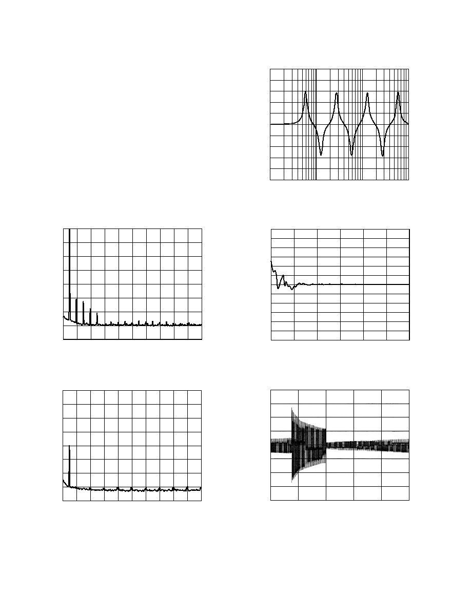
PERFORMANCE PLOTS
The following plots demonstrate the performance achieved on the
actual silicon. TPC 1 shows an FFT of a full-scale 1 kHz signal
with a THD+N of ≠100 dB, which is dominated by a second
harmonic. TPC 2 shows an FFT of a ≠60 dB sine wave, demon-
strating the lack of low level artifacts. TPC 3 shows a frequency
response plot with the seven equalization biquads set to an alter-
nating pattern of 6 dB boosts and cuts. TPC 4 shows a linearity
plot, where the measurement was taken with the same equaliza-
tion curve used to make TPC 3. When the biquad filters are not
in use, the signal passes through the filters with no quantization
effects. TPC 4 therefore demonstrates that using double-precision
math in the biquad filters has virtually eliminated any quantization
artifacts. TPC 5 shows a tone-burst applied to the compressor,
with the attack and recovery characteristics plainly visible. The
rms detector was programmed for normal rms time constants;
the hold/decay feature was not used for this plot.
0
≠160
0
20
2
4
6
8
14
16
18
≠20
≠80
≠120
≠40
≠60
≠100
≠140
10
12
kHz
dB
TPC 1. FFT of Full-Scale Sine Wave (32k Points)
0
≠160
0
20
2
4
6
8
14
16
18
≠20
≠80
≠120
≠40
≠60
≠100
≠140
10
12
kHz
dB
TPC 2. FFT of ≠60 dB Sine Wave (32k Points)
Hz
0
≠20
20
10k
≠10
1k
100
≠2
≠4
≠6
≠8
≠12
≠14
≠16
≠18
50
200
500
5k
dB
TPC 3. Frequency Response of EQ Biquad Filters
3.0
≠3.0
≠120
0
≠100
≠80
≠20
0.5
≠1.0
≠2.0
0
≠0.5
≠1.5
≠2.5
≠60
≠40
dBFS
2.5
1.5
2.0
1.0
dB
TPC 4. Linearity Plot
≠2.0
≠120
0
≠100
≠80
≠20
≠60
ms
≠1.5
≠1.0
≠0.5
0
0.5
1.0
1.5
2.0
V
TPC 5. Tone-Burst Response with Compressor
Threshold Set to ≠20 dB
REV. 0
AD1953
≠9≠
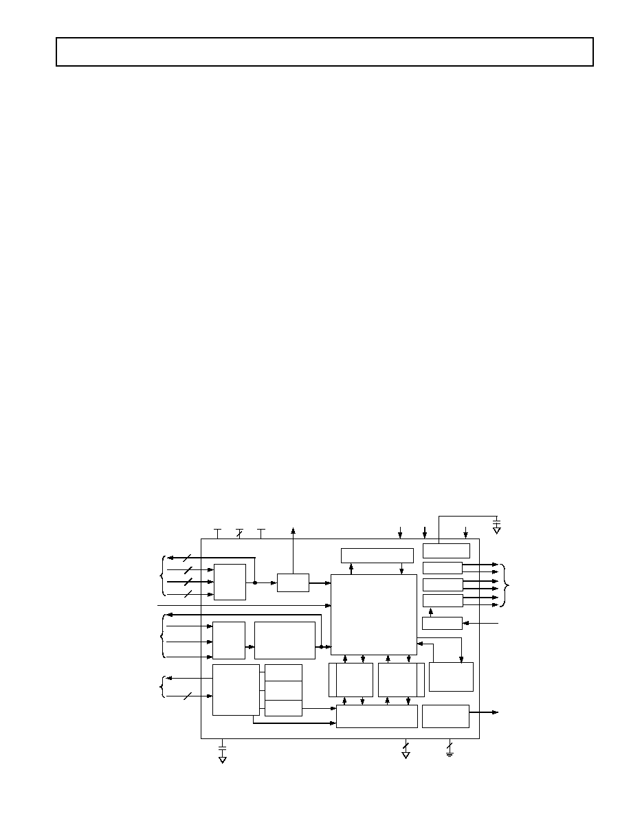
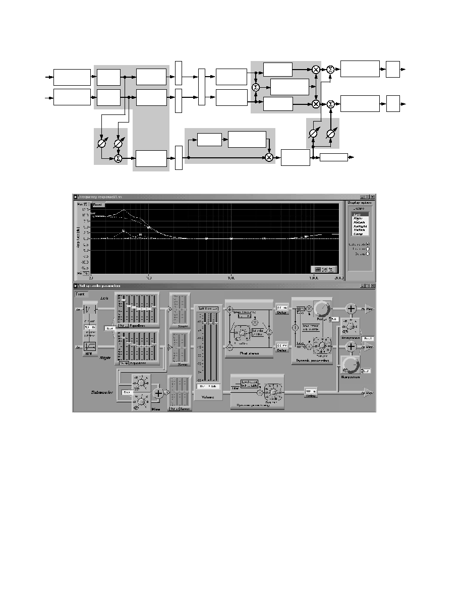
PRODUCT OVERVIEW (continued from page 1)
An extensive SPI port allows click-free parameter updates, along
with readback capability from any point in the algorithm flow.
The AD1953 also includes ADI's patented multibit
- DAC
architecture. This architecture provides 112 dB SNR and dynamic
range and THD+N of ≠100 dB. These specifications allow the
AD1953 to be used in applications ranging from low end
boom-boxes to high end professional mixing/editing systems.
The AD1953 has a digital output that allows it to be used purely
as a DSP. This digital output can also be used to drive an exter-
nal DAC to extend the number of channels beyond the three
that are provided on the chip. This chip can be used with either
its default signal processing program or with a custom user-
designed program. Graphical programming tools are available
from ADI for custom programming.
Features
The AD1953 is comprised of a 26-bit DSP (48-bit with double-
precision) for interpolation and audio processing, three multibit
- modulators, and analog output drive circuitry. Other features
include an on-chip parameter RAM using a "safe-upload" feature
for transparent and simultaneous updates of filter coefficients.
Digital de-emphasis filters are also included. On-chip input
selectors allow up to three sources of serial data and master
clock to be selected. The 3-channel configuration is especially
useful for 2.1 playback systems that include two satellite speakers
and a subwoofer. The default program allows for independent
equalization and compression/limiting for the satellite and
subwoofer outputs. Figure 1 shows the block diagram of the device.
The AD1953 contains a program RAM that is booted from an
internal program ROM on power-up. Signal-processing param-
eters are stored in a 256-location parameter RAM, which is
initialized on power-up by an internal boot ROM. New values
are written to the parameter RAM using the SPI port. The
values stored in the parameter RAM control the IIR equalization
filters, the dual-band compressor/limiter, the delay values, and
the settings of the stereo spreading algorithm.
The AD1953 has a very sophisticated SPI port that supports
complete read/write capability of both the program RAM and
the parameter RAM. Two control registers are also provided to
control the chip serial modes and various other optional fea-
tures. Handshaking is included for ease of memory uploads/
downloads.
The AD1953 contains eight independent data-capture circuits
that can be programmed to tap the signal flow of the processor
at any point in the DSP algorithm flow. Two of these data-
capture circuits can be read back over the SPI port, and the
other six are fed to a serial output pin operating either in TDM
mode (for all six channels) or 2-channel mode for simple con-
nection to an external DAC. This allows the basic functionality
of the AD1953 to be easily extended.
The processor core in the AD1953 has been designed from the
ground up for straightforward coding of sophisticated compres-
sion/limiting algorithms. The AD1953 contains two independent
compressor/limiters with rms based amplitude detection and
attack/hold/release controls, together with an arbitrary compres-
sion curve that is loaded by the user into a lookup table that
resides in the parameter RAM. The compressor also features
look-ahead compression, which prevents compressor overshoots.
The AD1953 has a very flexible serial data input port that allows
for glueless interconnection to a variety of ADCs, DSP chips,
AES/EBU receivers, and sample rate converters. The AD1953
can be configured in left-justified, I
2
S, right-justified, or DSP
serial port compatible modes. It can support 16, 20, and 24 bits
in all modes. The AD1953 accepts serial audio data in MSB
first, twos complement format. The part can also be set up in a
4-channel serial input mode by simultaneously using the serial
input mux and the auxiliary serial input.
The AD1953 operates from a single 5 V power supply. It is
fabricated on a single monolithic integrated circuit and is housed
in a 48-lead LQFP package for operation over the temperature
range ≠40
∞C to +105∞C.
3:1
AUDIO
DATA
MUX
1
3
3
SPI PORT
3:1
MCLK
MUX
1
MCLK
GENERATOR
1
(256/512 f
S
IN)
256/512 f
S
OUT
DAC ≠ L
COEFFICIENT
ROM
64 22
26 22
DSP CORE
DATA FORMAT:
3.23 (SINGLE PRECISION)
3.45 (DOUBLE PRECISION)
3
3
ANALOG
OUTPUTS
MASTER
CLOCK I/O
GROUP
DCSOUT
SPI I/O
GROUP
3
SERIAL
IN
1
DATA MEMORY, 512 26
CONTROL
REGISTERS
TRAP REG.
(I
2
S, SPI)
SAFELOAD
REGISTERS
PROGRAM
RAM
512 35
PARAMETER
RAM
256 22
BOO
T R
OM
MEMORY CONTROLLERS
DAC ≠ R
DAC ≠SW
2
BIAS
ANALOG
BIAS
RESETB MUTE
DE-EMPHASIS
ZEROFLAG
NOTES
1
CONTROLLED THROUGH SPI CONTROL REGISTERS
2
DAC DOES NOT USE DIGITAL INTERPOLATION
SERIAL DATA I/O
GROUP
DCSOUT TRAP
AUX SERIAL
DATA INPUT
(2-CHANNEL
AND TDM)
FILTCAP
AGND
3
DGND
2
VOLTAGE
REFERENCE
VREF
DVDD AVDD ODVDD
3
BOO
T R
OM
Figure 1. Block Diagram

REV. 0
AD1953
≠10≠
Pin Functions
All input pins have a logic threshold compatible with TTL input
levels, and may therefore be used in systems with 3.3 V logic.
All digital output levels are controlled by the ODVDD pin,
which may range from 2.7 V to 5.5 V, for compatibility with a
wide range of external devices. (See Pin Function Descriptions.)
SDATA0, 1, 2--Serial Data Inputs.
One of these three inputs is selected by an internal MUX, set by
writing to Bits <7:6> in Control Register 2. Default is 00, which
selects SDATA0. The serial format is selected by writing to Bits
<3:0> of Control Register 0. See SPI Read/Write Data Formats
section for recommendations on how to change input sources
without causing a click or pop noise.
LRCLK0, 1, 2--Left/Right Clocks for Framing the Input Data.
The active LRCLK input is selected by writing to Bits <7:6>
in Control Register 2. Default is 00, which selects LRCLK0.
The interpretation of the LRCLK changes according to the serial
mode, set by writing to Control Register 0.
BCLK0, 1, 2--Serial Bit Clocks for Clocking in the Serial Data.
The active BCLK input is selected by writing to Bits <7:6> in
Control Register 2. Default is 00, which selects BCLK0. The
interpretation of BCLK changes according to the serial mode,
which is set by writing to Control Register 0.
DMUXO/TDMO, LRMUXO/TDMFS, BMUXO/TDMBC
Dual-function pins:
∑ Function 1: Outputs of 3:1 MUX that selects one of the
three serial input groups.
∑ Function 2: Used for 6-channel data capture outputs in
TDM Data Capture Mode.
These three pins operate as MUX outputs when Bit <8> of
Control Register 2 is a 1 and Bits <13:12> of Control Register 1
are 00. These pins may be used to send the selected serial input
signals to other external devices. The default is OFF.
In TDM mode, TDMBC provides a 256
◊
f
S
clock signal,
TDMFS provides a frame sync signal, and TDMO provides the
TDM data for an external multichannel DAC or CODEC, such
as the AD1833 or AD1836 respectively. These output pins are
enabled by writing a 01 to Bits <13:12> of Control Register 1.
The default mode is 00, or OFF.
In TDM mode, the internal signals that are captured are con-
trolled by writing Program Counter Trap numbers to SPI
addresses 268 to 273. When the internal Program Counter
contents are equal to the Trap values written to the SPI port, the
selected DSP register is transferred to parallel-to-serial registers
and shifted out of the TDMO pin.
MCLK0, 1, 2--Master Clock Inputs.
Active input selected by writing to Bits <5:4> of Control Regis-
ter 2. The default is 00, which selects MCLK0. The master clock
frequency must be either 256
◊ f
S
or 512
◊ f
S
, where f
S
is the input
sampling rate. The master clock frequency is programmed by
writing to Bit <2> of Control Register 2. The default is 0, (512
◊ f
S
). See Initialization section for recommendations concerning
how to change clock sources without causing an audio click or
pop. Note that since the default MCLK source pin is MCLK0,
there must be a clock signal present on this pin on power-up so
that the AD1953 can complete its initialization routine.
MCLKO--Master Clock Output.
The master clock output pin may be programmed to produce
either 256
◊ f
S
, 512
◊ f
S
, or a copy of the selected MCLK input
pin. This pin is programmed by writing to Bits <1:0> of Control
Register 2. The default is 00, which disables the MCLKO pin.
CDATA--Serial Data In for the SPI Control Port.
See SPI Port section for more information on SPI port timing.
COUT--Serial Data Output.
This is used for reading back registers and memory locations. It
is three-stated when an SPI read is not active. See SPI Port
section for more information on SPI port timing.
CCLK--SPI Bit Rate Clock.
This pin either may run continuously or be gated off between
SPI transactions. See SPI Port section for more information on
SPI port timing.
CLATCH--SPI Latch Signal.
This pin must go LOW at the beginning of an SPI transaction,
and HIGH at the end of a transaction. Each SPI transaction
may take a different number of CCLKs to complete, depending
on the address and read/write bit that are sent at the beginning
of the SPI transaction. Detailed SPI timing information is given
in the SPI Port section.
RESETB--Active-Low Reset Signal.
After RESETB goes HIGH, the AD1953 goes through an ini-
tialization sequence where the program and parameter RAMs
are initialized with the contents of the on-board boot ROMs. All
SPI registers are set to 0, and the data RAMs are also zeroed.
The initialization is complete after 1024 MCLK cycles. Since
the MCLK IN FREQ SELECT (Bit <2> in Control Register 2)
defaults to 512
◊ f
S
at power-up, this initialization will proceed
at the external MCLK rate and will take 1024 MCLK cycles to
complete, regardless of the absolute frequency of the external
MCLK. New values should not be written to the SPI port until
the initialization is complete.
ZEROFLAG--Zero-Input Indicator.
This pin will go HIGH if both serial inputs have been inactive
(zero data) for 1024 LRCLK cycles. This pin may be used to
drive an external mute FET for reduced noise during digital
silence. This pin also functions as a test out pin, controlled by
the test register at SPI address 511. While most test modes are
not useful to the end user, one may be of some use. If the test
register is programmed with the number 7 (decimal), the
ZEROFLAG output will be switched to the output of the inter-
nal pseudo-random noise generator. This noise generator
operates at a bit rate of 128
◊ f
S
, and has a repeat time of once
per 2
24
cycles. This mode may be used to generate white noise
(or, with appropriate filtering, pink noise) to be used as a test
signal for measuring speakers or room acoustics.
DCSOUT--Data Capture Serial Out.
This pin will output the DSP's internal signals, which can be
used by external DACs or other signal-processing devices. The
signals that are captured and output on the DCSOUT pin are
controlled by writing Program Counter Trap numbers to SPI
addresses 263 (for the left output) and 264 (for the right output).
When the internal Program Counter contents are equal to the
Trap values written to the SPI port, the selected DSP register is
transferred to the DCSOUT parallel-to-serial registers and

REV. 0
AD1953
≠11≠
shifted out on the DCSOUT pin. Table XXI shows the Pro-
gram Counter Trap values and register-select values that should
be used to tap various internal points of the algorithm flow.
The DCSOUT pin is meant to be used in conjunction with the
LRCLK and BCLK signals that are provided to the serial input
port. The format of DCSOUT is the same as the format used
for the serial port. In other words, if the serial port is running in
I
2
S mode, then the DCSOUT pin, together with the LRCLK0
and BCLK0 pins (assuming input 0 is selected), will form a
valid 3-wire I
2
S output.
The DCSOUT pin can be used for a variety of purposes. If the
DCSOUT pin is used to drive another external DAC, then a 4.1
system is possible using a new program downloaded into the
program RAM.
AUXDATA--Auxiliary Serial Data Input.
The AUXDATA pin may be used in conjunction with a custom
program to access two extra channels of serial input data, allow-
ing for a total of four input channels. The serial format is identical
to the selected format of SDATA0, 1, 2. The AUXDATA pin is
synchronous to the selected LRCLK and BCLK signal, and there-
fore should have the same timing as the main serial input signal.
MUTE--Mute Output Signal.
When this pin is asserted HIGH, a ramp sequence is started that
gradually reduces the volume to zero. When deasserted, the
volume ramps from zero back to the original volume setting.
The ramp speed is timed so that it takes 10 ms to reach zero
volume when starting from the default 0 dB volume setting.
VOUTL+, VOUTL≠ --Left-Channel Differential Analog Out-
puts. Full-scale outputs correspond to 1 V rms on each output pin,
or 2 V rms differential, assuming a VREF input voltage of 2.5 V. The
full-scale swing scales directly with VREF. These outputs are
capable of driving a load of > 5 k
, with a maximum peak current
of 1 mA from each pin. An external third-order filter is recom-
mended for filtering out-of-band noise.
VOUTR+, VOUTR≠ --Right Channel Differential Outputs.
Output characteristics are the same as for VOUTL+ and VOUTL≠.
VOUTS+, VOUTS≠ --Sub Channel Differential Outputs.
These outputs are designed to drive loads of 10 k
or greater,
with a peak current capability of 250
µA. This output does not
use digital interpolation, as it is intended for low frequency
application. An external third-order filter with a cutoff frequency
< 2 kHz is recommended.
VREF--Analog Reference Voltage Input.
The nominal VREF input voltage is 2.5 V; the analog gain
scales directly with the voltage on this pin. When using the
AD1953 to drive a power amplifier, it is recommended that the
VREF voltage be derived by dividing down and heavily filtering
the supply to the power amplifier. This provides a benefit if the
compressor/limiter in the AD1953 is used to prevent amplifier
clipping. In this case, if the DAC output voltage is scaled to the
amplifier power supply, a fixed compressor threshold can be
used to protect an amplifier whose supply may vary over a wide
range. Any ac signal on this pin will cause distortion, and a large
decoupling capacitor may therefore be necessary to ensure that
the voltage on VREF is clean. The input impedance of VREF is
greater than 1 M
.
FILTCAP--Filter Capacitor Point.
This pin is used to reduce the noise on an internal biasing point
in order to provide the highest performance. It may not be nec-
essary to connect this pin, depending on the quality of the layout
and grounding used in the application circuit.
DVDD--Digital VDD for Core.
5 V nominal.
ODVDD--Digital VDD for All Digital Outputs.
Variable from 2.7 V to 5.5 V.
DGND (2)--Digital Ground.
AVDD (3)--Analog VDD.
5 V nominal. For best results, use a separate regulator for AVDD.
Bypass capacitors should be placed close to the pins and con-
nected directly to the analog ground plane.
AGND (3)--Analog Ground.
For best performance, separate nonoverlapping analog and
digital ground planes should be used.
REV. 0
AD1953
≠12≠
quality of compressed audio. In addition, the main channels
have a stereo widening algorithm that increases the perceived
spread of the stereo image.
Most of the signal processing functions are coded using full 48-bit
double-precision arithmetic. The input word length is 24 bits,
with two extra headroom bits added in the processor to allow
internal gains up to 12 dB without clipping (additional gains can
be accommodated by scaling down the input signal in the first
biquad filter section).
A graphical user interface (GUI) is available for evaluation of
the AD1953 (Figure 3). This GUI controls all of the functions
of the chip in a very straightforward and user-friendly interface.
No code needs to be written to use the GUI to control the chip.
For more information on AD1953 software tools, send an email to
SigmaDSP@analog.com.
SIGNAL PROCESSING
Signal Processing Overview
Figure 2 shows the signal processing flow diagram of the AD1953.
The AD1953 is designed to provide all common signal-processing
functions commonly used in 2.0 or 2.1 playback systems. A
7-biquad equalizer operates on the stereo input signal. The
output of this equalizer is fed to a 2-biquad crossover filter for
the main channels, and the mono sum of the left and right equalizer
outputs is fed to a 3-biquad crossover filter for the Sub channel.
Each of the three channels has independent delay compensa-
tion. There are two high quality compressor/limiters available:
one operating on the left/right outputs and one operating on the
subwoofer channel. The subwoofer output may be blended back
into the left/right outputs for 2.0 playback systems. In this
configuration, the two independent compressor/limiters provide
2-band compression, which significantly improves the sound
HPF/
DE-EMPHASIS
IN
RIGHT
IN
LEFT
VOLUME
VOLUME
PHAT STEREO
DELAY
(0ms≠3.7ms)
DELAY
(0ms≠3.7ms)
DELAY
(0ms≠2.3ms)
8
INTERPOLATION
DAC
OUT
LEFT
8
INTERPOLATION
DAC
OUT
RIGHT
VOLUME
1 BIQUAD
FILTER
DELAY
(0ms≠3.7ms)
MONO DAC
L/R REINJECTION
LEVEL
SUBWOOFER
OUTPUT
SUB DYNAMICS PROCESSOR
SUB CHANNEL
L/R MIX
EQ AND CROSSOVER FILTERS
L/R DYNAMICS PROCESSOR
LEVEL DETECT,
LOOK-UP TABLE
LEVEL DETECT,
LOOK-UP TABLE
7 BIQUAD
FILTERS
7 BIQUAD
FILTERS
CROSSOVER
(2 FILTERS)
CROSSOVER
(2 FILTERS)
CROSSOVER
(3 FILTERS)
DELAY
(0ms≠2.3ms)
HPF/
DE-EMPHASIS
Figure 2. Signal Processing Flow
Figure 3. Graphical User Interface
REV. 0
AD1953
≠13≠
Each section of this flow diagram will be explained in detail on
the following pages.
Numeric Formats
It is common in DSP systems to use a standardized method of
specifying numeric formats. To better comprehend issues relat-
ing to precision and overflow, it is helpful to think in terms of
fractional twos complement number systems. Fractional
number systems are specified by an A.B format, where A is the
number of bits to the left of the decimal point and B is the
number of bits to the right of the decimal point. In a twos
complement system, there is also an implied offset of one-half of
the binary range; for example, in a twos complement 1.23 sys-
tem, the legal signal range is ≠1.0 to (+1.0 ≠ 1 LSB).
The AD1953 uses two different numeric formats; one for the
coefficient values (stored in the parameter RAM) and one for
the signal data values. The coefficient format is as follows:
Coefficient Format
Coefficient format: 2.20
Range: ≠2.0 to (+2.0 ≠ 1 LSB)
Examples:
1000000000000000000000 = ≠2.0
1100000000000000000000 = ≠1.0
1111111111111111111111 = (1 LSB below 0.0)
0000000000000000000000 = 0.0
0100000000000000000000 = 1.0
0111111111111111111111 = (2.0 ≠ 1 LSB)
This format is used because standard biquad filters require
coefficients that range between +2.0 and ≠2.0. It also allows
gain to be inserted at various places in the signal path.
Internal DSP Signal Data Format
Input data format: 1.23
This is sign-extended when written to the data memory of the
AD1953.
Internal DSP signal data format: 3.23
Range: ≠4.0 to (+4.0 ≠ 1 LSB)
Examples:
10000000000000000000000000 = ≠4.0
11000000000000000000000000 = ≠2.0
11100000000000000000000000 = ≠1.0
11111111111111111111111111 = (1 LSB below 0.0)
00000000000000000000000000 = 0.0
00100000000000000000000000 = 1.0
01000000000000000000000000 = 2.0
01111111111111111111111111 = (4.0 ≠ 1 LSB).
The sign-extension between the serial port and the DSP core
allows for up to 12 dB of gain in the signal path without internal
clipping. Gains greater than 12 dB can be accommodated by
scaling the input down in the first biquad filter, and scaling the
signal back up at the end of the biquad filter section.
A digital clipper circuit is used between the output of the DSP
core and the input to the DAC
- modulators to prevent over-
loading the DAC circuitry (see Figure 4). Note that there is a
gain factor of 0.75 used in the DAC interpolation filters, and
therefore signal values of up to 1/0.75 will pass through the DSP
without clipping. Since the DAC is designed to produce an
analog output of 2 V rms (differential) with a 0 dB digital input,
signals between 0 dB and 1/0.75 (approximately 3 dB) will produce
larger analog outputs and result in slightly degraded analog per-
formance. This extra analog range is necessary in order to pass 0
dBFS square waves through the system, as these square waves
cause overshoots in the interpolation filters that would otherwise
briefly clip the digital DAC circuitry.
A separate digital clipper circuit is used in the DSP core to
ensure that any accumulator values that exceed the numeric
3.23 format range are clipped when taken from the accumulator.
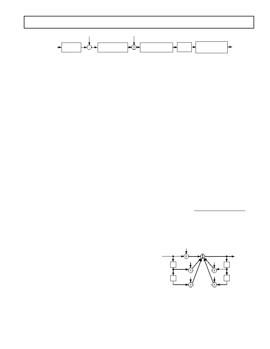
High-Pass Filter
The high-pass filter is a first-order double-precision design. The
purpose of the high-pass filter is to remove digital dc from the
input. If this dc were allowed to pass, the detectors used in the
compressor/limiter would give an incorrect reading for low
signal levels.
The high-pass filter is controlled by a single parameter
(alpha_HPF), which is programmed by writing to SPI location
180 in 2.20 twos complement format. The following equation
can be used to calculate the parameter Alpha_HPF from the ≠3 dB
point of the filter:
Alpha
HPF
EXP
HPF CUTOFF
f
S
_
. ≠
≠ .
_
=
◊ ◊
1 0
2 0
where EXP is the exponential operator, HPF_CUTOFF is the
high-pass cutoff in Hz, and f
S
is the audio sampling rate.
The default value for the ≠3 dB cutoff of the high-pass filter is
2.75 Hz at a sampling rate of 44.1 kHz.
b0
IN
OUT
b1
b2
a1
a2
Z
≠1
Z
≠1
Z
≠1
Z
≠1
Figure 5. Biquad Filter
Biquad Filters
Each of the two input channels has seven second-order biquad
sections in the signal path. In addition, the left and right chan-
nels have two additional biquad filters that may be used either
as crossover filters or as additional equalization filters. The sub
channel has three additional biquad filters, also to be used as
equalization and/or crossover filters. In a typical scenario, the
SIGNAL PROCESSING
(3.23 FORMAT)
SERIAL PORT
DAC INTERPOLATION
FILTERS (3.23 FORMAT)
DIGITAL -
MODULATORS
(1.23 FORMAT)
DIGITAL
CLIPPER
DATA IN
2-BIT SIGN EXTENTION
0.75
1.23
3.23
Figure 4. Numeric Precision and Clipping Structure

REV. 0
AD1953
≠14≠
first seven biquads would be used for speaker equalization and/
or tone controls, and the remaining filters would be programmed
to function as crossover filters. Note that there is a common
equalization section used for both the main and sub channels,
followed by crossover filters. This arrangement prevents any
interaction from occurring between the crossover filters and the
equalization filters. One section of the biquad IIR filter is shown
in Figure 5.
This section implements the transfer function:
H Z
b
b
Z
b
Z
a
Z
a
Z
( )
=
+ ◊
+
◊
(
)
-
◊
◊
(
)
0
1
2
1
1
2
1
2
1
2
≠
≠
≠
≠
≠
The coefficients a1, a2, b0, b1, and b2 are all in twos comple-
ment 2.20 format with a range from ≠2 to (+2 ≠ 1 LSB). The
negative sign on the a1 and a2 coefficients is the result of adding
both the feed-forward "b" terms as well as the feedback "a" terms.
Some digital filter packages automatically produce the correct
a1 and a2 coefficients for the topology of Figure 5, while others
assume a denominator of the form 1 + a1
◊ Z
≠1
+ a2
◊ Z
≠1
. In this
case, it may be necessary to invert the a1 and a2 terms for
proper operation.
The biquad structure shown in Figure 5 is coded using double-
precision math to avoid limit cycles from occurring when low
frequency filters are used. The coefficients are programmed by
writing to the appropriate location in the parameter RAM through
the SPI port (see Table VI). There are two possible scenarios
for controlling the biquad filters:
1. Dynamic Adjustment (for example, Bass/Treble control or Para-
metric Equalizer)
When using dynamic filter adjustment, it is highly recommended
that the user employ the safeload mechanism to avoid temporary
instability when the filters are dynamically updated. This can
occur if some, but not all, of the coefficients are updated to new
values when the DSP calculates the filter output. The operation
of the Safeload registers is detailed in the Options for Parameter
Updates section.
2. Setting Static EQ Curve after Power-Up
If many of the biquad filters need to be initialized after power-
up (for example, to implement a static speaker-correction
curve), the recommended procedure is to set the processor
shutdown bit, wait for the volume to ramp down (about 20 ms),
and then write directly to the parameter RAM in Burst
Mode. After the RAM is loaded, the shutdown bit can be
deasserted, causing the volume to ramp back up to the initial
value. This entire procedure is click-free and faster than using
the Safeload mechanism.
The datapaths of the AD1953 contain an extra two bits on top
of the 24 bits that are input to the serial port. This allows up to
12 dB of boost without clipping. However, it is important to
remember that it is possible to design a filter that has less than
12 dB of gain at the final filter output, but more than 12 dB of
gain at the output of one or more intermediate biquad filter
sections. For this reason, it is important to cascade the filter
sections in the correct order, putting the sections with the
largest peak gains at the end of the chain rather than at the
beginning. This is standard practice when coding IIR filters and
is covered in basic books on DSP coding.
If gains larger than 12 dB cannot be avoided, then the coeffi-
cients b0 through b2 of the first biquad section may be scaled
down to fit the signal into the 12 dB maximum signal range, and
then scaled back up at the end of the filter chain.
Volume
Eight separate SPI registers are available to control the volume.
Three registers are used by the on-board program--one each for
the Left, Right, and Sub channels. These registers are special in
that they include automatic digital ramp circuitry for clickless
volume adjustment. The volume control word is in 2.20 format,
and gains from +2.0 to ≠2.0 are possible. The default value is
1.0. It takes 1024 audio frames to adjust the volume from 2.0
down to 0; in the normal case where the max volume is set to
1.0, it will take 512 audio frames for this ramp to reach zero.
Note that a Mute command is the same as setting the volume to
zero, except that when the part is unmuted, the volume returns to
its original value. These volume ramp times assume that the
AD1953 is set for the fast volume ramp speed. If the slow
setting is selected, it will take 8192 audio frames to reach zero
from a setting of 2.0. Correspondingly, it will take 4096 frames
to reach 0 volume from the normal setting of 1.0.
The volume blocks are placed after the biquad filter sections to
maximize the level of the signal that is passed through the filter
sections. In a typical situation, the nominal volume setting might be
≠15 dB, allowing a substantial increase in volume when the user
increases the volume. The AD1953 was designed with an analog
dynamic range of > 112 dB, so that in the typical situation with
the volume set to ≠15 dB, the signal-to-noise ratio at the output
will still exceed 97 dB. Greater output dynamic ranges are possible
if the compressor/limiter is used, as the post-compression gain
parameter can boost the signal back up to a higher level. In this
case, the compressor will prevent the output from clipping when
the volume is turned up and the input signal is large.
Stereo Image Expander
The image-enhancement processing is based on ADI's patented
Phat Stereo algorithm. The block diagram is shown in Figure 6.
1kHz
FIRST-ORDER LPF
LEVEL
LEFT IN
RIGHT IN
LEFT OUT
RIGHT OUT
+
+
≠
≠
≠
Figure 6. Stereo Image Expander
The algorithm works by increasing the phase shift for low
frequency signals that are panned left or right in the stereo mix.
Since the ear is responsive to interaural phase shifts below 1 kHz,
this increase in phase shifts results in a widening of the stereo
image. Note that signals panned to the center are not processed,
resulting in a more natural sound. There are two parameters
that control the Phat Stereo algorithm: the Level variable,
which controls how much out-of-phase information is added to
the left and right channels, and the cutoff frequency of the
first-order low-pass filter, which determines the frequency range
of the added out-of-phase signals. For best results, the cutoff
frequency should be in the range of 500 Hz to 2 kHz. These
parameters are controlled by altering the parameter RAM locations
that store the parameters spread_level and alpha_spread.

REV. 0
AD1953
≠15≠
The spread_level is a linear number in 2.20 format that multiplies
the processed left-right signal before it is added to or subtracted
from the main channels. The parameter alpha_spread is related to
the cutoff frequency of the first-order low-pass filter by the equation
Alpha spread
EXP
spread
freq
f
S
_
. ≠
≠ .
_
=
◊ ◊
1 0
2 0
where EXP is the exponential operator, spread_freq is the low-pass
cutoff in Hz, and f
S
is the audio sampling rate.
Note that the stereo spreading algorithm assumes that frequencies
below 1 kHz are present in the main satellite speakers. In some
systems, the crossover frequency between the satellite and
subwoofer speakers is quite high (> 500 Hz). In this case, the
stereo spreading algorithm will not be effective, as the frequencies
that contribute to the spreading effect will be coming mostly from
the subwoofer, which is a mono source.
Delay
Each of the three DAC channels has a delay block that allows
the user to introduce a delay of up to 165 audio samples. The
delay values are programmed by entering the delay (in samples)
into the appropriate location of the parameter RAM. With a
44.1 kHz sample rate, a delay of 165 samples corresponds to a
time delay of 3.74 ms. Since sound travels at approximately
1 foot/ms, this can be used to compensate for speaker place-
ments that are off by as much as 3.74 feet.
An additional 100 samples of delay are used in the look-ahead
portion of the compressor/limiter, but only for the main two
channels. This can be used to increase the total delay for the left
and right channels to 265 samples, or 6 ms at 44.1 kHz.
Main Compressor/Limiter
The compressor used in the AD1953 is quite sophisticated and
is comparable in many ways to professional compressor/limiters
used in the professional audio and broadcast fields. It uses rms/
peak detection with adjustable attack/hold/release, look-ahead
compression, and table-based entry of the input/output curve for
complete flexibility.
The AD1953 uses two compressor/limiters, one in the subwoofer
DAC and one in the main left/right DAC. It is well known that
having independent compressors operating over different frequency
ranges results in a superior perceived sound. With a single-band
compressor, loud bass information will modulate the gain of the
entire audio signal, resulting in suboptimal maximum perceived
loudness as well as gain pumping or modulation effects. With
independent compressors operating separately on the low and
high frequencies, this problem is dramatically reduced. If the
AD1953 is being operated in 2-channel mode, an extra path is
added so that the subwoofer channel can be added back into the
main channel. This maintains the advantage of using a 2-band
compressor, even in a 2.0 system configuration.
Figure 7 shows the traditional basic analog compressor/limiter.
It uses a voltage controlled amplifier to adjust gain and a feed-
forward detector path using an rms detector with adjustable
time constants, followed by a nonlinear circuit to implement the
desired input/output relationship. A simple compressor will have
a single threshold above which the gain is reduced. The amount
of compression above the threshold is called the compression
ratio and is defined as dB change in input/dB change in output.
For example, if the input to a 2:1 compressor is increased by
2 dB, the output will rise by 1 dB for signals above the threshold.
A single "hard" threshold results in more audible behavior than
a so-called "soft-knee" compressor, where the compression is
introduced more gradually. In an analog compressor, the soft-knee
characteristic is usually made by using diodes in their exponential
turn-on region.
FILTER
RMS DETECTOR
WITH dB OUT
COMPRESSION
CURVE NON-
LINEAR CIRCUITS
THRESHOLD
SLOPE
VCA WITH EXP
CONTROL
OUT
Figure 7. Analog Compressor
The best analog compressors use rms detection as the signal
amplitude detector. RMS detectors are the only class of detec-
tors that are not sensitive to the phase of the harmonics in a
complex signal. The ear also bases its loudness judgment on the
overall signal power. Using an rms detector therefore results in
the best audible performance. Compressors that are based on
peak detection, while good for preventing clipping, are generally
quite poor when it comes to audible performance.
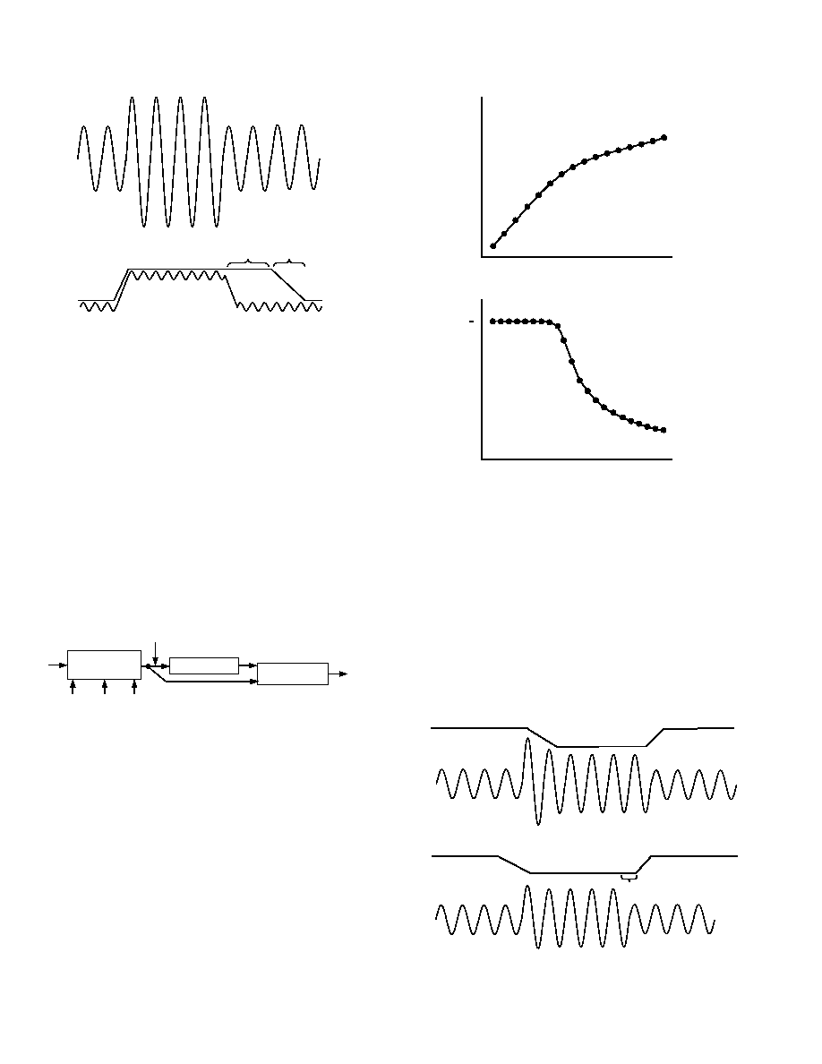
RMS detectors have a certain time constant that determines
how rapidly they can respond to transient signals. There is always
a trade-off between speed of response and distortion. Figure 8
shows this trade-off.
INPUT WAVEFORM
COMPRESSOR ENVELOPE ≠
FAST TIME CONSTANT
COMPRESSOR ENVELOPE ≠
SLOW TIME CONSTANT
Figure 8. Effect of RMS Time Constant on Distortion
In the case of a fast-responding rms detector, the detector enve-
lope will have a signal component in addition to the desired dc
component. This signal component (which, for an rms detector,
is at twice the input frequency) will result in harmonic distortion
when multiplied by this detector signal.
The AD1953 uses a modified rms algorithm to improve the
relationship between acquisition time and distortion. It uses a
peak-riding circuit together with a hold circuit to modify the rms
signal, as shown in Figure 9. Figure 8 shows two envelopes--one
with the harmonic distortion and another, flatter envelope,
which is produced by the AD1953.
REV. 0
AD1953
≠16≠
INPUT WAVEFORM
HOLD TIME, SPI-
PROGRAMMABLE
RELEASE TIME, SPI-
PROGRAMMABLE
Figure 9. Using the Hold and Release Time Feature
Using this idea of a modified rms algorithm, the true rms value
is still obtained for all but the lowest frequency signals, while the
distortion due to rms ripple is reduced. It also allows the user to
set the hold and release times of the compressor independently.
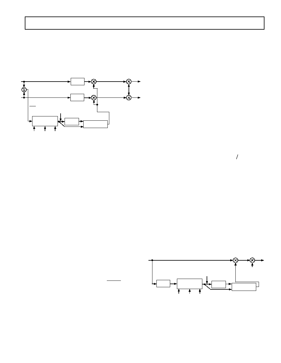
The detector path of the AD1953 is shown in Figure 10. The rms
detector is controlled by three parameters stored in parameter
RAM: the rms time constant, the hold time, and the release rate.
The log output of the rms detector is applied to a look-up table
with interpolation. The higher bits of the rms output form an
offset into this table, and the lower bits are used to interpolate
between the table entries to form a high precision gain word.
The look-up table resides in the parameter RAM and is loaded
by the user to give the desired curve. The look-up table contains
33 data locations, and the LSB of the address into the look-up
table corresponds to a 3 dB change in the amplitude of the detec-
tor signal. This gives the user the ability to program an input/
output curve over a 99 dB range. For the main compressor, the
table resides in locations 110 to 142 in the SPI parameter RAM.
LOOK-UP TABLE
LINEAR
INTERPOLATION
MODIFIED RMS
DETECTOR WITH
LOG OUTPUT
OUTPUT TO
GAIN STAGE
HIGH BITS (1LSB = 3dB)
LOW BITS
TIME
CONSTANT
HOLD
RELEASE
Figure 10. Gain Derived from Interpolated Look-Up Table
One subtlety of the table look-up involves the difference between
the rms value of a sine wave and that of a square wave. If a
full-scale square wave is applied to the AD1953, the rms value of
this signal will be 3 dB higher than the rms value of a 0 dBFS sine
wave. Therefore, the table will range from +9 dB (location 142)
to ≠87 dB (location 110).
The entries in the table are linear gain words in 2.20 format.
Figure 11 shows an example of the table entries for a simple
above-threshold compressor.
INPUT LEVEL ≠ 3dB/TABLE ENTRY
OUTPUT LEVEL ≠ dB
INPUT LEVEL ≠ 3dB/TABLE ENTRY
LINEAR GAIN
1.0
DESIRED
COMPRESSION
CURVE
Figure 11. Example of Table Entry for a Given
Compression Curve
Note that the maximum gain that can be entered in the table is 2.0
(minus 1 LSB). If more gain is required, the entire compression
curve may be shifted upward by using the post-compression gain
block following the compressor/limiter.
The AD1953 compressor/limiter also includes a look-ahead
compression feature. The idea behind look-ahead compression
is to prevent compressor overshoots by applying some digital
delay to the signal before the gain-control multiplier, but not to
the detector path. In this way, the detector can acquire the new
amplitude of the input signal before the signal actually reaches
the multiplier. A comparison of a tone burst fed to a conventional
compressor versus a look-ahead compressor is shown in Figure 12.
CONVENTIONAL COMPRESSOR GAIN
LOOK-AHEAD COMPRESSOR GAIN
HOLD TIME
Figure 12. Conventional Compression vs. Look-Ahead
Compression
REV. 0
AD1953
≠17≠
In the look-ahead compressor, the gain has already been reduced
by the time the tone-burst signal arrives at the multiplier input.
Note that when using a look-ahead compressor, it is impor-
tant to set the detector hold time to a value that is at least the
same as the look-ahead delay time, or else the compressor
release will start too soon, resulting in an expanded "tail" of a
tone burst signal. The complete flow of the left/right dynamics
processor is shown in Figure 13.
LOOK-UP
TABLE
LINEAR
INTERPOLATION
MODIFIED RMS
DETECTOR WITH
LOG OUTPUT
HIGH BITS (1LSB = 3dB)
LOW BITS
TIME
CONSTANT
HOLD
RELEASE
DELAY
DELAY
SPI-PROGRAMMABLE
LOOK-AHEAD DELAY
POST-COMPRESSION
GAIN, SPI-
PROGRAMMABLE
UP TO 30dB
2
(L+R)
Figure 13. Complete Dynamics Flow, Main Channels
The detector path works from a sum of left and right channels
((L+R)/2). This is the normal way that compressors are built,
and it counts on the fact that the main instruments in any stereo
mix are seldom recorded deliberately out of phase, especially in
the lower frequencies, which tend to dominate the energy spectrum
of real music.
The compressor is followed by a block known as post-compression
gain. Most compressors are used to reduce the dynamic range of
music by lowering the gain during loud signal passages. This
results in an overall loss of volume. This loss can be made up by
introducing gain after the compressor. In the AD1953, the
coefficient format used is 2.20, which has a maximum floating-
point representation of slightly less than 2.0. This means the
maximum gain that can be achieved in a single instruction is 6 dB.
To get more gain, the program in the AD1953 uses a cascade
of five multipliers to achieve up to 30 dB of post-compression gain.
To program the compressor/limiter, the following formulas may
be used to determine the 22-bit numbers (in 2.20 format) to be
entered into the parameter RAM.
RMS Time Constant
This can be best expressed by entering the time constant in
terms of dB/sec "raw" release rate (without the peak-riding circuit).
The attack rate is a rather complicated formula that depends on
the change in amplitude of the input sine wave.
rms tconst
parameter
release rate
f
S
_
_
. ≠
.
=
◊
1 0 10
10 0
where
rms_tconst_parameter = fractional number to enter into the
SPI RAM (after converting to 22-bit 2.20 format)
release_rate = release rate of the raw rms detector in dB/sec. This
must be negative. f
S
= audio sampling rate.
RMS Hold Time
rms holdtime
parameter
f
hold time
S
_
_
int
_
=
◊
(
)
where
rms_holdtime_parameter = integer number to enter into the SPI RAM
f
S
= audio sample rate
Hold_time = absolute time to wait before starting the release
ramp-down of the detector output
int() = integer part of expression
RMS Release Rate
rms decay
parameter
rms decay
_
_
int
_
/ .
=
(
)
1 096
Where rms_decay_parameter = decimal integer number to enter
into the SPI RAM
rms_decay = decay rate in dB/sec
int() = integer part of expression
Look-Ahead Delay
Lookahead delay
parameter
Lookahead delay
f
S
_
_
_
=
◊
Where Lookahead_delay = predictive compressor delay in abso-
lute time
f
S
= audio sample rate
The maximum Lookahead_delay_parameter value is 100.
Post-Compression Gain
Post
compression
gain
parameter
Post
compression
gain
linear
_
_
_
_
_
_
=
( )
1 5
Where Post_compression gain_linear is the linear post-compression
gain
^ = raise to the power
Subwoofer Compressor/Limiter
The subwoofer compressor/limiter differs from the left/right
compressor in the following ways:
1. The subwoofer compressor operates on a weighted sum of left
and right inputs (aa
◊ Left + bb ◊ Right), where aa and bb are
both programmable.
2. The detector input has a biquad filter in series with the input
in order to implement frequency-dependent compression
thresholds.
3. There is no predictive compression, as presumably the input
signals are filtered to pass only low frequencies, and therefore
transient overshoots are not a problem.
The subwoofer compressor signal flow is shown in Figure 14.
LOOK-UP
TABLE
LINEAR
INTERPOLATION
MODIFIED RMS
DETECTOR WITH
LOG OUTPUT
HIGH BITS (1LSB = 3dB)
LOW BITS
TIME
CONSTANT
HOLD
RELEASE
V
IN
_SUB = K1 LEFT_IN + K2 RIGHT_IN
POST-COMPRESSION
GAIN, SPI-
PROGRAMMABLE
UP TO 30dB
BIQUAD
FILTER
Figure 14. Signal Flow for Subwoofer Compressor
The biquad filter before the detector can be used to implement
a frequency-dependent compression threshold. For example,
assume that the overload point of the woofer is strongly fre-
quency-dependent. In this case, one would have to set the
compressor threshold to a value that corresponded to the most
sensitive overload frequency of the woofer. If the input signal
happened to be mostly in a frequency range where the woofer

REV. 0
AD1953
≠18≠
was not so sensitive to overload, then the compressor would be
too pessimistic and the volume of the woofer would be reduced.
If, on the other hand, the biquad filter were designed to follow
the woofer excursion curve of the speaker, then the volume of
the woofer could be maximized under all conditions. This is
illustrated in Figure 15.
20Hz
200Hz
FREQ
W
OOFER EXCURSION
BIQ
U
AD RESPONSE
20Hz
200Hz
FREQ
Figure 15. Optimizing Woofer Loudness Using the
Subwoofer RMS Biquad Filter
When using a filter in front of the detector, a confusing side-
effect occurs. If one measures the frequency response by using a
swept sine wave with an amplitude large enough to be above the
compressor threshold, the resulting frequency response will not
look flat. However, this is not real in the sense that, as the sine
wave is swept through the system, the gain is being slowly
modulated up and down according to the response of the biquad
filter in front of the detector. If one measures the response using a
pink-noise generator, the result will look much better, as the
detector will settle on only one gain value. The perceptual effect
of the swept-sine-wave test is not at all what would be pre-
dicted by simply looking at the frequency response curve; it is
only the signal-path filters that will affect the perception of fre-
quency response, not the detector-path filters.
De-emphasis Filtering
The standard for encoding CDs allows the use of a pre-emphasis
curve during encoding, which must be compensated for by a
de-emphasis curve during playback. The de-emphasis curve is
defined as a first-order shelving filter with a single pole at
(1/(2
◊ ◊ 50 µs)) followed by a single zero at (1/(2 ◊ ◊ 15 µs)).
This curve may be accurately modeled using a first-order digital
filter. This filter is included in the AD1953; it is not part of the
bank of biquad filters, and so does not take away from the num-
ber of available filters.
Since the specification of the de-emphasis filter is based on an
analog filter, the response of the filter should not depend on the
incoming sampling rate. However, when the de-emphasis filter is
implemented digitally, the response will scale with the sampling rate
unless the filter coefficients are altered to suit each possible input
sampling rate. For this reason, the AD1953 includes three separate
de-emphasis curves; one each for sampling rates of 32 kHz, 44.1 kHz,
and 48 kHz. These curves are selected by writing to Bits <5:4> of
Control Register 1 over the SPI port.
Using the Sub Reinjection Paths for Systems with No Subwoofer
Many systems will not use a subwoofer, but would still benefit
from 2-band compression/limiting. This can be accommodated
by using sub reinjection paths in the program flow. These
parameters are programmed by entering two numbers (in 2.20
format) into the parameter RAM. Note that if the biquad filters
are not properly designed, the frequency response at the cross-
over point may not be flat. Many crossover filters are designed to
be flat in the sense of adding the powers together, but nonflat if
the sum is done in voltage mode. The user must take care to
design an appropriate set of crossover filters.
Interpolation Filters
The left and right channels have a 128:1 interpolation filter
with 70 dB stop-band attenuation that precedes the digital
-
modulator. This filter has a group delay of approximately 24.185/f
S
,
where f
S
is the sampling rate. The sub channel does not use an
interpolation filter. The reason for this (besides saving valuable
MIPS) is that it is expected that the bandwidth of the sub output
will be limited to less than 1 kHz. With no interpolation filter, the
first "image" will therefore be at 43.1 kHz (which is f
S
≠ 1 kHz,
for CD audio). The standard external filter used for both the
main and sub channels is a third-order, single op amp filter. If
the cutoff frequency of the external subwoofer filter is 2 kHz,
then there are more than four octaves between 2 kHz and the
first image at 43.1 kHz. A third-order filter will roll off by
approximately 18 dB/oct
◊ 4 octaves = 72 dB attenuation. This is
approximately the same as the digital attenuation used in the main
channel filters, so no internal interpolation filter is required to remove
the out-of-band images.
Note that by having interpolation filters in the main channels but
not the subwoofer channel, there is a potential time-delay mis-
match between the main and sub channels. The group delay of
the digital interpolation filters used in the main left/right channels
is about 0.5 ms. This must be compared to the group delay of
the external analog filter used in the subwoofer path. If the
group delay mismatch causes a frequency response error (when the
two signals are "acoustically added"), the programmable delay
feature can be used to put extra delay in either the subwoofer path
or the main left/right path.
SPI PORT
Overview
The AD1953 has many different control options. Most signal-
processing parameters are controlled by writing new values to
the parameter RAM using the SPI port. Other functions such as
volume and de-emphasis filtering are programmed by writing to
SPI control registers.
The SPI port uses a 4-wire interface, consisting of CLATCH,
CCLK, CDATA, and COUT signals. The CLATCH signal
goes LOW at the beginning of a transaction and HIGH at the
end of a transaction. The CCLK signal latches the serial input
data on a low-to-high transition. The CDATA signal carries the
serial input data, and the COUT signal is the serial output data.
The COUT signal remains three-stated until a read operation is
requested. This allows other SPI compatible peripherals to
share the same readback line.
The SPI port is capable of full read/write operation for all of the
memories (parameter and program) and some of the SPI registers
(Control Register 1 and data capture registers). The memories
may be accessed in both a single-address mode or in burst mode.
All SPI transactions follow the same basic format, shown in Table I.
The Wb/R bit is low for a write, and high for a read operation.
The 10-bit address word is decoded into a location in one of the
two memories (parameter or program) or one of the SPI regis-
ters. The number of data bytes varies according to the register
or memory being accessed. In burst-write mode (available for
loading the RAMs only), an initial address is given followed by a
continuous sequence of data for consecutive RAM locations.

REV. 0
AD1953
≠19≠
The detailed data format diagram for continuous-mode opera-
tion is given in SPI Read/Write data formats.
A sample timing diagram for a single SPI WRITE operation to
the parameter RAM is shown in Figure 16.
Table I. SPI Word Format
Byte 0
Byte 1
Byte 2
Byte 3
Byte 4
00000, R/Wb, adr[9:8]
Adr[7:0]
Data
Data
Data
A sample timing diagram of a single SPI READ operation is
shown in Figure 17. The COUT pin goes from three-state to
driven at the beginning of Byte 2. Bytes 0 and 1 contain the
address and R/W bit, and Bytes 2 to 4 carry the data. The exact
format is shown in Tables VIII to XIX.
The AD1953 has several mechanisms for updating signal-
processing parameters in real time without causing loud pops or
clicks. In cases where large blocks of data need to be downloaded,
the DSP core can be shut down and new data loaded, and the
core can then be restarted. The shutdown and restart mecha-
nisms employ a gradual volume ramp to prevent clicks and pops.
In cases where only a few parameters need to be changed (for
example, a single biquad filter), a safeload mechanism is used
that allows a block of SPI registers to be transferred to the
parameter RAM within a single audio frame while the core is
running. The safeload mode uses internal logic to prevent con-
tention between the DSP core and the SPI port.
SPI Address Decoding
Table II shows the address decoding used in the SPI port. The
SPI address space encompasses a set of registers and two RAMs,
one for holding signal-processing parameters and one for holding
the program instructions. Both of the RAMs are loaded on
power-up from on-board boot ROMs.
BYTE 0
BYTE 1
BYTE 4
CDATA
CCLK
CLATCH
Figure 16. Sample of SPI WRITE Format (Single-Write Mode)
BYTE 0
CDATA
CCLK
CLATCH
COUT
BYTE 1
HI-Z
DATA
XXX
DATA
DATA
HI-Z
Figure 17. Sample of SPI READ Format (Single-Read Mode)

REV. 0
AD1953
≠20≠
Table II. SPI Port Address Decoding
SPI Address
Register Name
Read/Write Word Length
0≠255
Parameter RAM
Write: 22 Bits
Read: 22 Bits
256
SPI Control Register 1
Write: 14 Bits
Read: 2 Bits
257
SPI Control Register 2
Write: 10 Bits
Read: N/A
258
Volume 0
Write: 22 Bits
Read: N/A
259
Volume 1
Write: 22 Bits
Read: N/A
260
Volume 2
Write: 22 Bits
Read: N/A
261
Volume 3
Write: 22 Bits
Read: N/A
262
Volume 4
Write: 22 Bits
Read: N/A
263
Volume 5
Write: 22 Bits
Read: N/A
264
Volume 6
Write: 22 Bits
Read: N/A
265
Volume 7
Write: 22 Bits
Read: N/A
266
Data Capture (SPI Out) #1
Write: 9-Bit Program Counter Value, 2-Bit Register Address
Read: 24 Bits
267
Data Capture (SPI Out) #2
Write: 9-Bit Program Counter Value, 2-Bit Register Address
Read: 24 Bits
268
Data Capture (Serial Out) Slot 0
Write: 9-Bit Program Counter Value, 2-Bit Register Address
Read: N/A
269
Data Capture (Serial Out) Slot 1
Write: 9-Bit Program Counter Value, 2-Bit Register Address
Read: N/A
270
Data Capture (Serial Out) Slot 2
Write: 9-Bit Program Counter Value, 2-Bit Register Address
Read: N/A
271
Data Capture (Serial Out) Slot 3
Write: 9-Bit Program Counter Value, 2-Bit Register Address
Read: N/A
272
Data Capture (Serial Out) Slot 4
Write: 9-Bit Program Counter Value, 2-Bit Register Address
Read: N/A
273
Data Capture (Serial Out) Slot 5
Write: 9-Bit Program Counter Value, 2-Bit Register Address
Read: N/A
274
Parameter RAM Safeload Register 0
Write: 8-Bit Parameter RAM Address, 22-Bit Parameter Data
Read: N/A
275
Parameter RAM Safeload Register 1
Write: 8-Bit Parameter RAM Address, 22-Bit Parameter Data
Read: N/A
276
Parameter RAM Safeload Register 2
Write: 8-Bit Parameter RAM Address, 22-Bit Parameter Data
Read: N/A
277
Parameter RAM Safeload Register 3
Write: 8-Bit Parameter RAM Address, 22-Bit Parameter Data
Read: N/A
278
Parameter RAM Safeload Register 4
Write: 8-Bit Parameter RAM Address, 22-Bit Parameter Data
Read: N/A
279≠510
Unused
511
Test Register
Write: 8 Bits
Read: N/A
512≠1024
Program RAM
Write: 35 Bits
Read: 35 Bits

REV. 0
AD1953
≠21≠
Control Register 1
Control Register 1 is a 14-bit register that controls data capture
modes, serial modes, de-emphasis, mute, power-down, and
SPI-to-memory transfers. Table III documents the contents of
this register. Table IV details the two bits in the register's
read operation.
Bits <1:0> set the wordlength, which is used in right-justified
serial modes to determine where the MSB is located relative to
the start of the audio frame.
Bits <3:2> select one of four serial modes, which are discussed
in the Serial Data Input Port section.
The de-emphasis curve selection Bits <5:4> turn on the internal
de-emphasis filter for one of three possible sample rates.
Bit <6>, the soft power-down bit, stops the internal clocks to
the DSP core, but does not reset the part. The digital power
consumption is reduced to a low level when this bit is asserted.
Reset can only be asserted using the external reset pin.
Soft mute (Bit <7>) is used to initiate a volume ramp-down
sequence. If the initial volume was set to 1.0, this operation will
take 512 audio frames to complete. When this bit is deasserted,
a ramp-up sequence is initiated until the volume returns to its
original setting.
The initiate-safe-transfer Bit <9> will request a data transfer
from the SPI safeload registers to the parameter RAM. The
safeload registers contain address-data pairs, and only those
registers that have been written to since the last transfer opera-
tion will be uploaded. The user may poll for this operation being
complete by reading Bit <0> of Control Register 1. The Safeload
Mechanism section goes into more detail on this feature.
Bit <10>, the halt program bit, is used to initiate a volume
ramp-down followed by a shutdown of the DSP core. The user
may poll for this operation being complete by reading Bit <1>
of Control Register 1.
The Data Capture Serial Out mode is controlled with Bits
<13:12>. This function can be used to send data that is cap-
tured using the data-capture feature to external devices such as
an external stereo DAC or multichannel codec. The Data Cap-
ture Registers and Outputs section gives more information about
the TDM and data capture features.
Table III. Control Register 1 Write Definition
Register Bits
Function
13:12
Data Capture Serial Out Mode Control
00 = none
01 = TDM 6-channel out, uses Pins 41≠43
10 = 2-channel out, uses Pin 45
11 = Unused
11
Unused
10
Halt Program (1 = Halt)
9
Initiate Safe Transfer (1 = Transfer)
8
Unused
7
Soft Mute (1 = Start Mute Sequence)
6
Soft Power-Down (1 = Power Down)
5:4
De-emphasis Curve Select
00 = none
01 = 44.1 kHz
10 = 32 kHz
11 = 48 kHz
3:2
Serial In Mode
00 = I
2
S
01 = Right-Justified
10 = DSP
11 = Left-Justified
1:0
Word Length
00 = 24 Bits
01 = 20 Bits
10 = 16 Bits
11 = 16 Bits

REV. 0
AD1953
≠22≠
Table IV. Control Register 1 READ Definition
Register Bits
Function
1
DSP Core Shutdown Complete
1 = Shutdown Complete
0 = Not Shut Down
0
Safe Memory Load Complete
1 = Complete (Note: Cleared after Read)
0 = Not Complete
Bit 0 is asserted when all requested safeload registers have been
transferred to the parameter RAM. It is cleared after the read
operation is complete.
Bit 1 is asserted after the requested shutdown of the DSP is
completed. When this bit is set, the user is free to write or read
any RAM location without causing an audio pop or click.
Table V. Control Register 2 WRITE Definition
Register Bits
Function
9
Volume Ramp Speed
1 = 160 ms Full-Ramp Time
0 = 20 ms Full-Ramp Time
8
Serial Port Output Enable
1 = Enabled
0 = Disabled
7:6
Serial Port Input Select
00 = IN0
01 = IN1
10 = IN2
11 = NA
5:4
MCLK Input Select
00 = MCLK0
01 = MCLK1
10 = MCLK2
11 = NA
3
Reserved
2
MCLK In Frequency Select
0 = 512
◊ f
S
1 = 256
◊ f
S
1:0
MCLK Out Frequency Select
00 Disabled
01 512
◊ f
S
10 256
◊ f
S
11 MCLKO = MCLK_In (Feedthrough)
Control Register 2
Table V documents the contents of Control Register 2. Bits
<1:0> set the frequency of the MCLKO pin. If these bits are set
to 00, the MCLKO pin is disabled (default). When set to 01,
the MCLKO pin is set to 512
◊ f
S
, which is the same as the
internal master clock used by the DSP core. When set to 10,
this pin is set to 256
◊ f
S
, derived by dividing the internal DSP
clock by 2. In this mode, the output 256
◊ f
S
clock will be inverted
with respect to the input 256
◊ f
S
clock. This is not the case with
the feedthrough mode. When set to 11, the MCLKO pin mirrors
the selected MCLK input pin (it's the output of the MCLK
MUX selector). Note that the internal DSP master clock may
either be the same as the selected MCLK pin (when MCLK
frequency select is set to 512
◊ f
S
mode) or may be derived from
the MCLK pin using internal clock doubler (when MCLK fre-
quency select is set to 256
◊ f
S
)
.
Bit <2> selects one of two possible MCLK input frequencies. When
set to 0 (default), the MCLK frequency is set to 512
◊ f
S
. In this mode,
the internal DSP clock and the external MCLK are at the same
frequency. When set to 1, the MCLK frequency is set to 256
◊ f
S
, and
an internal clock doubler is used to generate the DSP clock.
Bits <5:4> select one of three clock input sources using an inter-
nal MUX. To avoid click and pop noises when switching MCLK
sources, it is recommended that the user put the DSP core in
shutdown before switching MCLK sources.
Bits <7:6> select one of three serial input sources using an inter-
nal MUX. Each source selection includes a separate SDATA,
LRCLK, and BCLK input. To avoid click and pop noises when
switching serial sources, it is recommended that the user put the
DSP core in shutdown before writing to these bits.
Bit <8> is used to enable the three serial output pins. These pins
are connected to the output of the serial input MUX, which is set
by Bits <7:6>. The default is 0 (disabled).
Bit <9> changes the default setting of the volume ramp speed.
When set to 0, it will take 1024 LRCLK periods to go from full
volume (6 dB) to infinite attention. When set to 1, the same
operation will take 8192 LRCLK periods.

REV. 0
AD1953
≠23≠
Volume Registers
The AD1953 contains eight 22-bit volume registers, one each
for the left, right, and subwoofer channels and an additional five
registers to be used by custom programs used in multichannel
applications. These registers are special because when the volume
is changed from an initial value to a new value, a linear ramp is
used to interpolate between the two values. This feature prevents
audible clicks and pops when changing volume. The ramp is
set so that it takes 512 audio frames to decrement from a volume of
1.0 (default) down to 0 (muted). The volume registers are for-
matted in 2.20 twos complement, meaning that 010000000
0000000000000 is interpreted as 1.0. Negative values can also be
written to the volume register, causing an inversion of the signal.
Negative values work as expected with the ramp feature; to go
from +1.0 to ≠1.0 will take 1024 LRCLKs, and the volume will
pass through 0 on the way.
Parameter RAM Contents
Table VI shows the contents of the parameter RAM. The
parameter RAM is 22 bits wide and occupies SPI addresses
0≠255. The low addresses of the RAM are used to control the
biquad filters. There are 22 biquad filters in all, and each
biquad has five coefficients, resulting in a total memory usage
of 110 coefficients. There are also two tables of 33 coefficients
each that define the main and sub compressor input/output
characteristics. These are loaded with 1.0 on power-up, resulting
in no compression. Other RAM entries control other compressor
characteristics, as well as delay and spatialization settings.
The parameter RAM is initialized on power-up by an on-board
boot ROM. The default values (shown in the table) yield no
equalization, no compression, no spatialization, no delay, and
"normal" detector time constants in the compressor sections.
The functionality of the AD1953 on power-up is basically that
of a normal audio DAC with no signal-processing capability.
The data format of the Parameter RAM is twos complement
2.20 format. This means that the coefficients may range from
+2.0 (≠1 LSB) to ≠2.0, with 1.0 represented by the binary word
0100000000000000000000.
Table VI. Parameter RAM Contents
Default Value
in Fractional
Address
Function
2.20 Format
0
IIR0 Left b0
1.0
1
IIR0 Left b1
0
2
IIR0 Left b2
0
3
IIR0 Left a1
0
4
IIR0 Left a2
0
5
IIR1 Left b0
1.0
6
IIR1 Left b1
0
7
IIR1 Left b2
0
8
IIR1 Left a1
0
9
IIR1 Left a2
0
10
IIR2 Left b0
1.0
11
IIR2 Left b1
0
12
IIR2 Left b2
0
13
IIR2 Left a1
0
14
IIR2 Left a2
0
15
IIR3 Left b0
1.0
16
IIR3 Left b1
0
17
IIR3 Left b2
0
18
IIR3 Left a1
0
19
IIR3 Left a2
0
20
IIR4 Left b0
1.0
21
IIR4 Left b1
0
22
IIR4 Left b2
0
23
IIR4 Left a1
0
24
IIR4 Left a2
0
25
IIR5 Left b0
1.0
26
IIR5 Left b1
0
27
IIR5 Left b2
0
28
IIR5 Left a1
0
29
IIR5 Left a2
0
30
IIR6 Left b0
1.0
31
IIR6 Left b1
0
32
IIR6 Left b2
0
33
IIR6 Left a1
0
34
IIR6 Left a2
0
35
IIR0 Right b0
1.0
Table VI. Parameter RAM Contents (continued)
Default Value
in Fractional
Address
Function
2.20 Format
36
IIR0 Right b1
0
37
IIR0 Right b2
0
38
IIR0 Right a1
0
39
IIR0 Right a2
0
40
IIR1 Right b0
1.0
41
IIR1 Right b1
0
42
IIR1 Right b2
0
43
IIR1 Right a1
0
44
IIR1 Right a2
0
45
IIR2 Right b0
1.0
46
IIR2 Right b1
0
47
IIR2 Right b2
0
48
IIR2 Right a1
0
49
IIR2 Right a2
0
50
IIR3 Right b0
1.0
51
IIR3 Right b1
0
52
IIR3 Right b2
0
53
IIR3 Right a1
0
54
IIR3 Right a2
0
55
IIR4 Right b0
1.0
56
IIR4 Right b1
0
57
IIR4 Right b2
0
58
IIR4 Right a1
0
59
IIR4 Right a2
0
60
IIR5 Right b0
1.0
61
IIR5 Right b1
0
62
IIR5 Right b2
0
63
IIR5 Right a1
0
64
IIR5 Right a2
0
65
IIR6 Right b0
1.0
66
IIR6 Right b1
0
67
IIR6 Right b2
0
68
IIR6 Right a1
0
69
IIR6 Right a2
0
70
IIR0 Xover Left b0
1.0
71
IIR0 Xover Left b1
0

REV. 0
AD1953
≠24≠
Table VI. Parameter RAM Contents (continued)
Default Value
in Fractional
Address
Function
2.20 Format
72
IIR0 Xover Left b2
0
73
IIR0 Xover Left a1
0
74
IIR0 Xover Left a2
0
75
IIR1 Xover Left b0
1.0
76
IIR1 Xover Left b1
0
77
IIR1 Xover Left b2
0
78
IIR1 Xover Left a1
0
79
IIR1 Xover Left a2
0
80
IIR0 Xover Right b0
1.0
81
IIR0 Xover Right b1
0
82
IIR0 Xover Right b2
0
83
IIR0 Xover Right a1
0
84
IIR0 Xover Right a2
0
85
IIR1 Xover Right b0
1.0
86
IIR1 Xover Right b1
0
87
IIR1 Xover Right b2
0
88
IIR1 Xover Right a1
0
89
IIR1 Xover Right a2
0
90
IIR0 Xover Sub b0
1.0
91
IIR0 Xover Sub b1
0
92
IIR0 Xover Sub b2
0
93
IIR0 Xover Sub a1
0
94
IIR0 Xover Sub a2
0
95
IIR1 Xover Sub b0
1.0
96
IIR1 Xover Sub b1
0
97
IIR1 Xover Sub b2
0
98
IIR1 Xover Sub a1
0
99
IIR1 Xover Sub a2
0
100
IIR2 Xover Sub b0
1.0
101
IIR2 Xover Sub b1
0
102
IIR2 Xover Sub b2
0
103
IIR2 Xover Sub a1
0
104
IIR2 Xover Sub a2
0
105
IIR Sub rms b0
1.0
106
IIR Sub rms b1
0
107
IIR Sub rms b2
0
108
IIR Sub rms a1
0
109
IIR Sub rms a2
0
Table VI. Parameter RAM Contents (continued)
Default Value
in Fractional
Address
Function
2.20 Format
110≠142
Main Compressor
1.0 (all)
Look-Up Table Base
143
Main Compressor
5.75
10
≠4
Attack/rms Time
(120 dB/sec)
Constant
144
Main Post-Compressor
1.0
Gain
145≠177
Subwoofer Compressor
1.0 (all)
Look-Up Table Base
178
Sub Compressor
5.75
10
≠4
Attack/RMS Time
(120 dB/sec)
Constant
179
Post-Compressor
1.0
Gain (SUB)
180
High-Pass Filter
3.92
10
≠4
Cutoff Frequency
181
Main Compressor
0
Look-Ahead Delay
182
Delay Left
0
183
Delay Right
0
184
Delay Sub
0
185
Stereo Spreading
0
Coefficient
186
Stereo Spreading
0.112694
Frequency Control
187
Subwoofer Reinjection
0.0
to Main Left
188
Subwoofer Reinjection
0.0
to Main Right
189
Subwoofer Channel
0.5
Input Gain from Left IN
190
Subwoofer Channel
0.5
Input Gain from Right IN
191
Main Detector Hold Time, 0
1
Samples (4095 MAX)
192
Sub Detector Hold Time,
0
1
Samples (4095 MAX)
193
Main Detector Decay Time 0x3FFFFF
(4.597 10
6
dB/sec)
1, 2
194
Sub Detector Decay Time
0x3FFFFF
(4.597 10
6
dB/sec)
1, 2
NOTES
1
The detector hold and decay times are integer values, while the rest of the parameters are fractional twos complement values.
2
The default decay time of the hold/release circuit is set fast enough that the decay is dominated by the time constant of the rms detector.
Options for Parameter Updates
The parameter and program RAMs can be written and read
using one of several methods.
1. Direct Read/Write. This method allows direct access to the
RAMs. Since the RAMs are also being used during real-time
DSP operation, a glitch will likely occur at the output. This
method is not recommended.
2. Direct Read/Write after Core Shutdown. This method avoids
the glitch while accessing the internal RAMs by first shutting
down the core. This is recommended for transferring large
amounts of data, such as initializing the parameter RAM at
power-up or downloading a completely new program. These
transfers can be sped up by using burst mode, where an
initial address followed by blocks of data are sent to the RAM.
3. Safeload Writes Up to five SPI registers are loaded with
address/data intended for the parameter RAM. The data is then
transferred to the requested address when the RAM is not busy.
This method can be used for dynamic updates while live
program material is playing through the AD1953. For example,
a complete update of one biquad section can occur in one
audio frame while the RAM is not busy. This method is not
available for writing to the program RAM or control registers.
The next section discusses these options in more detail.
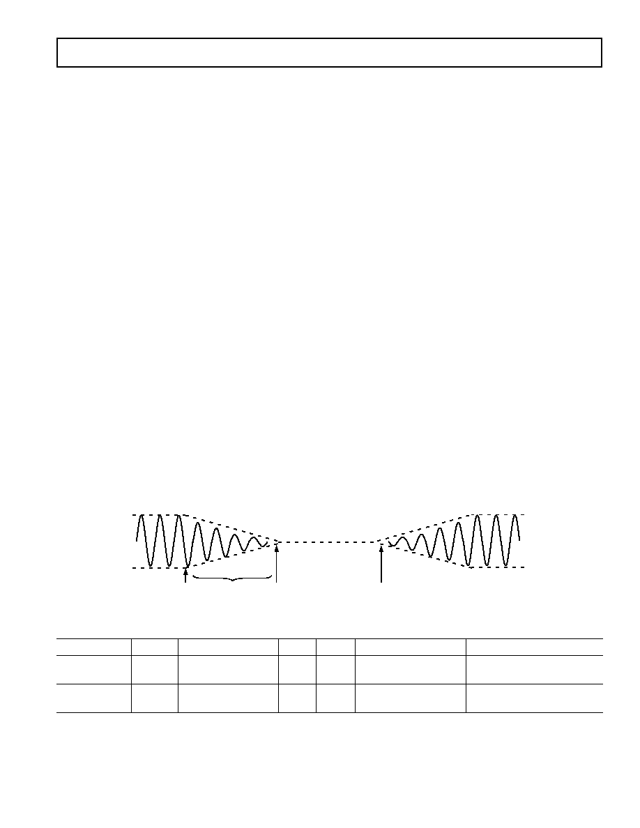
REV. 0
AD1953
≠25≠
Soft Shutdown Mechanism
When writing large amounts of data to the program or parameter
RAM, the processor core should be halted to prevent unpleasant
noises from appearing at the audio output. Figure 18 shows a
graphical representation of this mechanism's volume envelope.
Points A to D are referenced in the following description. Bit
<10> in serial Control Register 0 (processor shutdown bit) will
shut down the processor core. When the processor shutdown bit
is asserted (A), an automatic volume ramp-down sequence (B)
lasting from 10 ms to 20 ms will occur, followed by a shutdown
of the core. This method of shutting down the core prevents pops
or clicks from occurring. After the shutdown is complete, Bit
<1> in Control Register 1 will be set. The user can either poll
for this bit to be set, or just wait for a period longer than 20 ms.
Once the core is shut down (C), the parameter or program RAMs
may be written or read freely. To ease the transfer of large blocks
of sequential data, a block transfer mode is supported where a
starting address followed by a stream of data is sent to the memory.
The address into the memory will be automatically incremented
for each new write. This mode is documented in the SPI Data
Format section of this data sheet.
Once the data has been written, the shutdown bit can be cleared
(D). The processor then will initiate a volume ramp-up sequence
lasting 10 ms to 20 ms. Again, this reduces the chance that any
pop or click noise will occur.
Note that this shutdown sequence assumes the part is set to the
fast volume ramp speed (Control Register 2, Bit <9>). If the
slow ramp speed is set, the volume may not reach zero before
the part enters shutdown, and a click or pop may be heard.
Safeload Mechanism
Many applications require real-time control of filter characteristics,
such as bass/treble controls and parametric or graphic equaliza-
tion. To prevent instability from occurring, all of the parameters
of a particular biquad filter must be updated at the same time;
otherwise, the filter could execute for one or two audio frames
with a mixture of old and new coefficients. This mix of old and
new could cause temporary instability, leading to transients that
could take a long time to decay.
The method used in the AD1953 to eliminate this problem is to
load a set of five registers in the SPI port with the desired param-
eter RAM address and data. Five registers are used because each
biquad filter has five coefficients. Once these registers are loaded,
the initiate safe transfer bit in SPI Control Register 1 is set.
Once this bit is set, the processor waits for a period of time in
the program sequence when the parameter RAM is not being
accessed for at least five consecutive instruction cycles. When
the program counter reaches this point, the parameter RAM is
written with five new data values at addresses corresponding to
those entered in the safeload registers. When the operation is
complete, Bit 0 of Control Register 1 is set. This bit may be
polled by the external microprocessor until a 1 is read. This bit
will be reset on a read operation. The polling operation is not
required; the safeload mechanism guarantees that the transfer
will be complete within one audio frame.
The safeload logic automatically sends only those safeload regis-
ters that have been written to since the last safeload operation.
For example, if only two parameters are to be sent, it is only
necessary to write to two of the five safeload registers. When the
request safe transfer bit is asserted, only those two registers will
be sent; the other three registers are not sent, and can still hold
old or invalid data.
The safeload mechanism is not limited to uploading biquad
coefficients; any set of five values in the parameter RAM may be
updated in the same way. This allows real-time adjustment of
the compressor/limiter, delay, or stereo spreading blocks.
Summary of RAM Modes
Table VII shows the sizes and available modes of the parameter
RAM and the program RAM.
A
D
C
B
Figure 18. Recommended Sequences for Complete Parameter or Program RAM Upload Using Shutdown Mechanism
Table VII. Read/Write Modes
Memory
Size
SPI Address Range
Read
Write
Burst Mode Available
Write Modes
Parameter RAM
256
◊
22
0≠255
Yes
Yes
Yes
Direct Write, Write after core
shutdown, safeload write
Program RAM
512
◊
35
512≠1023
Yes
Yes
Yes
Direct Write, Write after core
shutdown
REV. 0
AD1953
≠26≠
Table VIII. Parameter RAM Read/Write Format (Single Address)
Byte 0
Byte 1
Byte 2
Byte 3
Byte 4
00000, R/Wb, Adr[9:8]
Adr[7:0]
00, Param[21:16]
Param[15:8]
Param[7:0]
ADR
Byte 5 Byte 8
Byte 6 Byte 9
Byte 7 Byte 10
ADR + 1 ADR + 2
Table IX. Parameter RAM Block Read/Write Format (Burst Mode)
Byte 0
Byte 1 Byte 2 Byte 3
Byte 4
00000, R/Wb, Adr[9:8]
Adr[7:0]
00, Param[21:16] Param[15:8]
Param[7:0]
Table X. Program RAM Read/Write Format (Single Address)
Byte 0
Byte 1
Byte 2
Byte 3
Byte 4
Byte 5
Byte 6
00000, R/Wb, Adr[9:8] Adr[7:0]
00000, Prog[34:32]
Prog[31:24]
Prog[23:16]
Prog[15:8]
Prog[7:0]
Table XI. Program RAM Block Read/Write Format (Burst Mode)
Byte 0
Byte 1
Byte 2
Byte 3
Byte 4
Byte 5
Byte 6
00000, R/Wb, Adr[9:8]Adr[7:0] 00000, Prog[34:32] Prog[31:24] Prog[23:16] Prog[15:8] Prog[7:0]
ADR
Byte 7 Byte 12
Byte 8 Byte 13
Byte 9 Byte 14
Byte 10 Byte 15
Byte 11 Byte 16
ADR + 1 ADR + 2
Table XII. SPI Control Register 1 Write Format
Byte 0
Byte 1
Byte 2
Byte 3
00000, R/Wb, Adr[9:8]
Adr[7:0]
00, Bit[13:8]
Bit[7:0]
Table XIII. SPI Control Register 1 Read Format
Byte 0
Byte 1
Byte 2
00000, R/Wb, Adr[9:8]
Adr[7:0]
000000, Bit[1:0]
Table XIV. SPI Control Register 2 Write Format
Byte 0
Byte 1
Byte 2
Byte 3
00000, R/Wb, Adr[9:8]
Adr[7:0]
000000, Bit[9:8]
Bit[7:0]
Table XV. SPI Volume Register Write Format
Byte 0
Byte 1
Byte 2
Byte 3
Byte 4
000000, Adr[9:8]
Adr[7:0]
00, Volume[21:16]
Volume[15:8]
Volume[7:0]
SPI READ/WRITE DATA FORMATS
The read/write formats of the SPI port are designed to be byte-
oriented. This allows for easy programming of common
microcontroller chips to fit into a byte-oriented format; 0s are
appended to the data fields to extend the data-word to the next
multiple of eight bits. For example, 22-bit words written to the
SPI parameter RAM are appended with two leading zeros to
reach 24 bits (three bytes), and 35-bit words written to the
program RAM are appended with five zeros to reach 40 bits
(five bytes). These zero-extended data fields are appended to
a 2-byte field consisting of a read/write bit and a 10-bit address.
The SPI port knows how many data bytes to expect based on
the address that is received in the first two bytes.
The total number of bytes for a single-location SPI write command
can vary from four bytes (for a control register write), to seven
bytes (for a program RAM write). Block writes may be used to
fill contiguous locations in program RAM or parameter RAM.
REV. 0
AD1953
≠27≠
Table XVI. Data Capture Register Write Format
Byte 0
Byte 1
Byte 2
Byte 3
00000, R/Wb, Adr[9:8]
Adr[7:0]
00000, ProgCount[8:6]
1
ProgCount[5:0], RegSel[1:0]
1, 2
NOTES
1. ProgCount[8:0] = value of program counter where trap occurs (see Table XXI).
2. RegSel[1:0] selects one of four registers (see Data Capture Register section).
Table XVII. Data_Capture_Serial Out Register (Address and Register Select) Write Format
Byte 0
Byte 1
Byte 2
Byte 3
00000, R/Wb, Adr[9:8]
Adr[7:0]
00000, ProgCount[8:6]
1
ProgCount[5:0], RegSel[1:0]
1, 2
NOTES
1. ProgCount[8:0] = value of program counter where trap occurs (see Table XXI).
2. RegSel[1:0] selects one of four registers (see Data Capture Registers section).
Table XVIII. Data Capture Read Format
Byte 0
Byte 1
Byte 2
Byte 3
Byte 4
Byte 5
00000, R/Wb, Adr[9:8]
Adr[7:0]
00000000
Data[23:16]
Data[15:8]
Data[7:0]
Table XIX. Safeload Register Write Format
Byte 0
Byte 1
Byte 2
Byte 3
Byte 4
Byte 5
00000, R/Wb, Adr[9:8]
Adr[7:0]
ParamAdr[7:0]
00, Param[21:16]
Param[15:8]
Param[7:0]
INITIALIZATION
Power-Up Sequence
The AD1953 has a built-in power-up sequence that initializes
the contents of all internal RAMs. During this time, the contents
of the internal program boot ROM are copied to the internal
program RAM, and likewise the SPI parameter RAM is filled
with values from its associated boot ROM. The data memories
are also cleared during this time.
The boot sequence lasts for 1024 MCLK cycles and starts on
the rising edge of the RESETB pin. Since the boot sequence
requires a stable master clock, the user should avoid writing to
or reading from the SPI registers during this period of time.
Note that the default power-on state of the internal clock mode
circuitry is 512
◊ f
S
, or about 24 MHz for normal audio sample
rates. This mode bypasses all the internal clock doublers and
allows the external master clock to directly operate the DSP
core. If the external master clock is 256
◊ f
S
, the boot sequence will
operate at this reduced clock rate and take slightly longer to
complete. After the boot sequence has finished, the clock modes
may be set via the SPI port. For example, if the external master
clock frequency is 256
◊ f
S
clock, the boot sequence would
take 1024 256
◊ f
S
clock cycles to complete, after which an
SPI write could occur to put the AD1953 in 256
◊ f
S
mode.
The default state of the MCLK input selector is MCLK0. Since
this input selector is controlled using the SPI port, and the SPI
port cannot be written to until the boot sequence is complete,
there must be a stable master clock signal present on the MCLK0
pin at startup.
Setting the Clock Mode
The AD1953 contains a clock doubler circuit that is used to
generate an internal 512
◊ f
S
clock when the external clock is
256
◊ f
S
. The clock mode is set by writing to Bit <2> of Control
Register 2.
When the clock mode is changed, it is possible that a glitch will
occur on the internal MCLK signal. This may cause the proces-
sor to inadvertently write an incorrect value into the data RAM,
which could cause an audio pop or click sound. To prevent this,
it is recommended that the following procedure be followed:
1. Assert the soft power-down bit (Bit <6> in Control Register 1)
to stop the internal MCLK.
2. Write the desired clock mode into Bit <2> of Control Register 2.
3. Wait at least 1 ms while the clock doublers settle.
4. Deassert the soft power-down bit.
An alternative procedure is to initiate a soft shutdown of the
processor core by writing a 1 to the halt program bit in Control
Register 1. This initiates a volume ramp-down sequence followed
by a shutdown of the DSP core. Once the core is shut down
(which can be verified by reading Bit <1> from Control Register 1,
or by waiting at least 20 ms), the new clock mode can be
programmed by writing to Bit <2> of Control Register 2. The
DSP core can then be restarted by clearing the halt program bit
in Control Register 1.

REV. 0
AD1953
≠28≠
Setting the Data and MCLK Input Selectors
The AD1953 contains input selectors for both the serial data
inputs as well as the MCLK input. This allows the AD1953 to
select a variety of input and clock sources with no external hard-
ware required. These input selectors are controlled by writing to
SPI Control Register 2.
When the DATA source or MCLK source is changed by writing
to the SPI port, it is possible that a pop or click will occur in the
audio. To prevent this noise, the core should be shut down by
writing a 1 to the "halt program" bit in Control Register 1. This
initiates a volume ramp-down sequence followed by a shutdown
of the DSP core. Once the core is shut down (which can be
verified by reading Bit <1> from Control Register 1, or by wait-
ing at least 20 ms after the halt program command is issued),
the new DATA or MCLK source can be programmed by writ-
ing to Control Register 2. The DSP core can then be restarted
by clearing the "halt-program" bit in Control Register 1.
DATA CAPTURE REGISTERS AND OUTPUTS
The AD1953 incorporates a feature called "data capture." Using
this feature, any node in the signal processing flow may be sent
either to an SPI-readable register, to a dedicated serial output
pin (2-channel output), or to a set of dual-function pins (6-channel
TDM mode). This allows the basic functionality of the AD1953
to be extended to a larger number of channels, or alternatively it
can be used to monitor and display information about signal
levels or compressor/limiter activity.
The AD1953 contains eight independent data capture registers.
The Data Capture SPI Out registers are used for reading back
internal DSP signals over the SPI port. These registers can be
used for a variety of purposes. One example might be to access
the dB output of the internal rms detector, to run a front-panel
signal level display.
The remaining data capture registers are used to output internal
DSP signals to external DACs, CODECs, or DSP chips. There
are two possible output modes, detailed in the following table.
Table XX. Data Capture/TDM Mode Settings
DMUXO/TDMO,
Control
DCSOUT
LRMUXO/TDMFS,
Reg 1, Bits Control Reg
Pin (45)
BMUXO/TDMBC
<13:12>
2, Bit <8>
Functions
Pin Functions
00
0
OFF
OFF
00
1
OFF
Serial MUX Output
01
Don't care
OFF
TDM Data Capture
Outputs and Clocks,
6-channel Output
10
0
ON, 2-
OFF
channel
output.
10
1
ON, 2-
Serial MUX Output
channel
output.
In TDM output mode, the Serial Mux Out multifunction pins
(41≠43) are used to output 6-channel TDM data, BCLK, and
frame sync signals. In 2-channel output mode, the data appears
on Pin 45, and can be used with the BCLK and LRCLK signals
that are already present on the serial input pins. The data will
be formatted in the same way as the input data. The data cap-
ture feature is primarily intended to feed signals to external
DACs, DSPs, or CODECs, such as the AD1836, in order to
extend the number of channels that the internal DSP can access.
For each of the data capture registers, a capture count and a
register select must be set. The capture count is a number between
0 and 511 that corresponds to the program step number where
the capture will occur. The register-select field programs one of
four registers in the DSP core that will be transferred to the data
capture register when the program counter equals the capture
count. The register select field is decoded as follows:
00: Multiplier Output (Mult_Out)
01: Output of dB conversion block (DB_OUT)
10: Multiplier Data Input (MDI)
11: Multiplier Coefficient Input (MCI)
The capture count and register select bits are set by writing to
one of the four data capture registers at the following SPI addresses:
266: SPI data capture setup register 1
267: SPI data capture setup register 2
268: Data Capture serial out setup register 0
269: Data Capture serial out setup register 1
270: Data Capture serial out setup register 2
271: Data Capture serial out setup register 3
272: Data Capture serial out setup register 4
273: Data Capture serial out setup register 5
The format of the captured data varies according to the register
select fields. Data captured from the Mult_Out setting is in 1.23
twos complement format, so that a full-scale input signal will
produce a full-scale digital output (assuming no processing). If
the parameters are set such that the input-to-output gain is
more than 0 dB, then the digital output will be clipped.
Data captured from the DB_OUT setting is in 5.19 format,
where the actual rms dB level is equal to ≠87 + (3
◊ DB_OUT).
In this equation, DB_OUT is the value that is captured. It
follows that in this data format, the actual output readings will
range from ≠87 dB to +9 dB. The AD1953 uses the convention
that 0 dB is the rms value of the full-scale digital signal.
Data captured using the MDI setting is in 3.21 format. A 0 dB
digital input will produce a ≠12 dB digital output, assuming the
AD1953 is set for no processing.
Data captured using the MCI setting is in 2.20 format. This data
is generally a signal gain or filter coefficient, and therefore it does
not make sense to talk about the input-to-output gain. A coeffi-
cient of 0100000000000000000000 corresponds to a gain of 1.0.
The data that must be written to set up the data capture is a
concatenation of the 9-bit program count index with the 2-bit
register select field.
The SPI capture registers can be accessed by reading from SPI
locations 266 (for SPI capture register 1) or 267 (for SPI capture
register 2). The other six data capture registers (data capture
serial-out) automatically transfer their data to either the Data
Capture Serial Out (DCSOUT) pin in 2-channel mode or the
DMUXO/TDMO pin in TDM mode. In 2-channel mode,
DCSOUT capture register 1 is present in the left data slot (as
defined by the serial input format) and DCSOUT capture regis-
ter 2 is present in the right data slot.

REV. 0
AD1953
≠29≠
Table XXI. Data Capture Trap Indexes and Register Select
Program Count
Signal Description
Index (9 Bits)
Register Select (2 Bits)
Numeric Format
HPF Out Left
15
Mult_Out
1.23, Clipped
HPF Out Right
259
Mult_Out
1.23, Clipped
De-emphasis Out Left
19
Mult_Out
1.23, Clipped
De-emphasis Out Right
263
Mult_Out
1.23, Clipped
Left Biquad 0 Output
34
Mult_Out
1.23, Clipped
Left Biquad 1 Output
43
Mult_Out
1.23, Clipped
Left Biquad 2 Output
52
Mult_Out
1.23, Clipped
Left Biquad 3 Output
61
Mult_Out
1.23, Clipped
Left Biquad 4 Output
70
Mult_Out
1.23, Clipped
Left Biquad 5 Output
79
Mult_Out
1.23, Clipped
Left Biquad 6 Output
88
Mult_Out
1.23, Clipped
Right Biquad 0 Output
284
Mult_Out
1.23, Clipped
Right Biquad 1 Output
293
Mult_Out
1.23, Clipped
Right Biquad 2 Output
302
Mult_Out
1.23, Clipped
Right Biquad 3 Output
311
Mult_Out
1.23, Clipped
Right Biquad 4 Output
320
Mult_Out
1.23, Clipped
Right Biquad 5 Output
329
Mult_Out
1.23, Clipped
Right Biquad 6 Output
338
Mult_Out
1.23, Clipped
Volume Out Left
114
Mult_Out
1.23, Clipped
Volume Out Right
111
Mult_Out
1.23, Clipped
Volume Out Sub
459
Mult_Out
1.23, Clipped
Phat Stereo Out Left
115
Mult_Out
1.23, Clipped
Phat Stereo Out Right
112
Mult_Out
1.23, Clipped
Delay Output Left
190
Mult_Out
1.23, Clipped
Delay Output Right
361
Mult_Out
1.23, Clipped
Main Compressor rms Out (dB)
154
DB_Out
24-Bit Positive Binary, Bit <19>
Corresponds to a 3 dB Change
Main Compressor Gain Reduction
165
MCI
2.22, 2 LSB = 0
(Linear)
Look-Ahead Delay Output Left
165
MDI
3.21, 2 LSBs truncated
Look-Ahead Delay Output Right
178
MDI
3.21, 2 LSBs truncated
Main Compressor Out Left
175
Mult_Out
1.23, Clipped
Main Compressor Out Right
188
Mult_Out
1.23, Clipped
Interpolator Input Left
191
Mult_Out
1.23, Clipped
(includes SUB Reinject)
Interpolator Input Right
362
Mult_Out
1.23, Clipped
(includes SUB Reinject)
Sub Channel Filter Input
430
Mult_Out
1.23, Clipped
Sub XOVER Biquad 0 Output
438
Mult_Out
1.23, Clipped
Sub XOVER Biquad 1 Output
447
Mult_Out
1.23, Clipped
Sub XOVER Biquad 2 Output
456
Mult_Out
1.23, Clipped
Left XOVER Biquad 0 Output
99
Mult_Out
1.23, Clipped
Left XOVER Biquad 1 Output
108
Mult_Out
1.23, Clipped
Right XOVER Biquad 0 Output
349
Mult_Out
1.23, Clipped
Right XOVER Biquad 1 Output
358
Mult_Out
1.23, Clipped
Sub Delay Output
511
Mult_Out
1.23, Clipped
Sub rms Biquad Output
467
Mult_Out
1.23, Clipped
Sub rms Output (dB)
489
DB_Out
24-Bit Positive Binary, Bit <19>
Corresponds to a 3 dB Change
Sub Compressor Gain (Linear)
495
MCI
2.22, 2 LSB = 0
Sub Channel Output
511
Mult_Out
1.23, Clipped
REV. 0
AD1953
≠30≠
SERIAL DATA INPUT/OUTPUT PORTS
The AD1953's flexible serial data input port accepts data in twos
complement, MSB first format. The left channel data field always
precedes the right channel data field. The serial mode is set by
using mode select bits in the SPI control register. In all modes
except for the right-justified mode, the serial port will accept an
arbitrary number of bits up to a limit of 24 (extra bits will not
cause an error, but they will be truncated internally). In the right-
justified mode, SPI control register bits are used to set the word
length to 16, 20, or 24 bits. The default on power-up is 24-bit mode.
Proper operation of the right-justified mode requires that there
be exactly 64 BCLK per audio frame.
Serial Data Input/Output Modes
Figure 19 shows the serial input modes. For the left-justified
mode, LRCLK is HIGH for the left channel, and LOW for the
right channel. Data is sampled on the rising edge of BCLK. The
MSB is left-justified to an LRCLK transition, with no MSB delay.
The left-justified mode can accept any word length up to 24 bits.
In I
2
S mode, LRCLK is low for the left channel and high for the
right channel. Data is valid on the rising edge of BCLK. The MSB
is left-justified to an LRCLK transition but with a single BCLK
period delay. The I
2
S mode can be used to accept any number
of bits up to 24.
In right-justified mode, LRCLK is high for the left channel and
low for the right channel. Data is sampled on the rising edge
of BCLK. The start of data is delayed from the LRCLK edge
by 16, 12, or 8 BCLK intervals, depending on the selected
word length. The default word length is 24 bits; other word
lengths are set by writing to Bits <1:0> of Control Register 1.
In right-justified mode, it is assumed that there are 64 BCLKs
per frame.
RIGHT CHANNEL
LEFT CHANNEL
LRCLK
BCLK
SDATA
LSB
LSB
LSB
LSB
LSB
LSB
LSB
LSB
LEFT CHANNEL
RIGHT CHANNEL
LRCLK
BCLK
SDATA
LRCLK
BCLK
SDATA
LRCLK
BCLK
SDATA
DSP MODE ≠ 16 BITS TO 24 BITS PER CHANNEL
NOTES
1. DSP MODE DOESN'T IDENTIFY CHANNEL
2. LRCLK NORMALLY OPERATES AT
f
S
EXCEPT DSP MODE, WHICH IS 2
f
S
3. BCLK FREQUENCY IS NORMALLY 64 LRCLK BUT MAY BE OPERATED IN BURST MODE
I
2
S MODE ≠ 16 BITS TO 24 BITS PER CHANNEL
RIGHT-JUSTIFIED MODE ≠ SELECT NUMBER OF BITS PER CHANNEL
1/
f
S
LEFT-JUSTIFIED MODE ≠ 16 BITS TO 24 BITS PER CHANNEL
MSB
MSB
MSB
MSB
MSB
MSB
MSB
MSB
Figure 19. Serial Input Modes
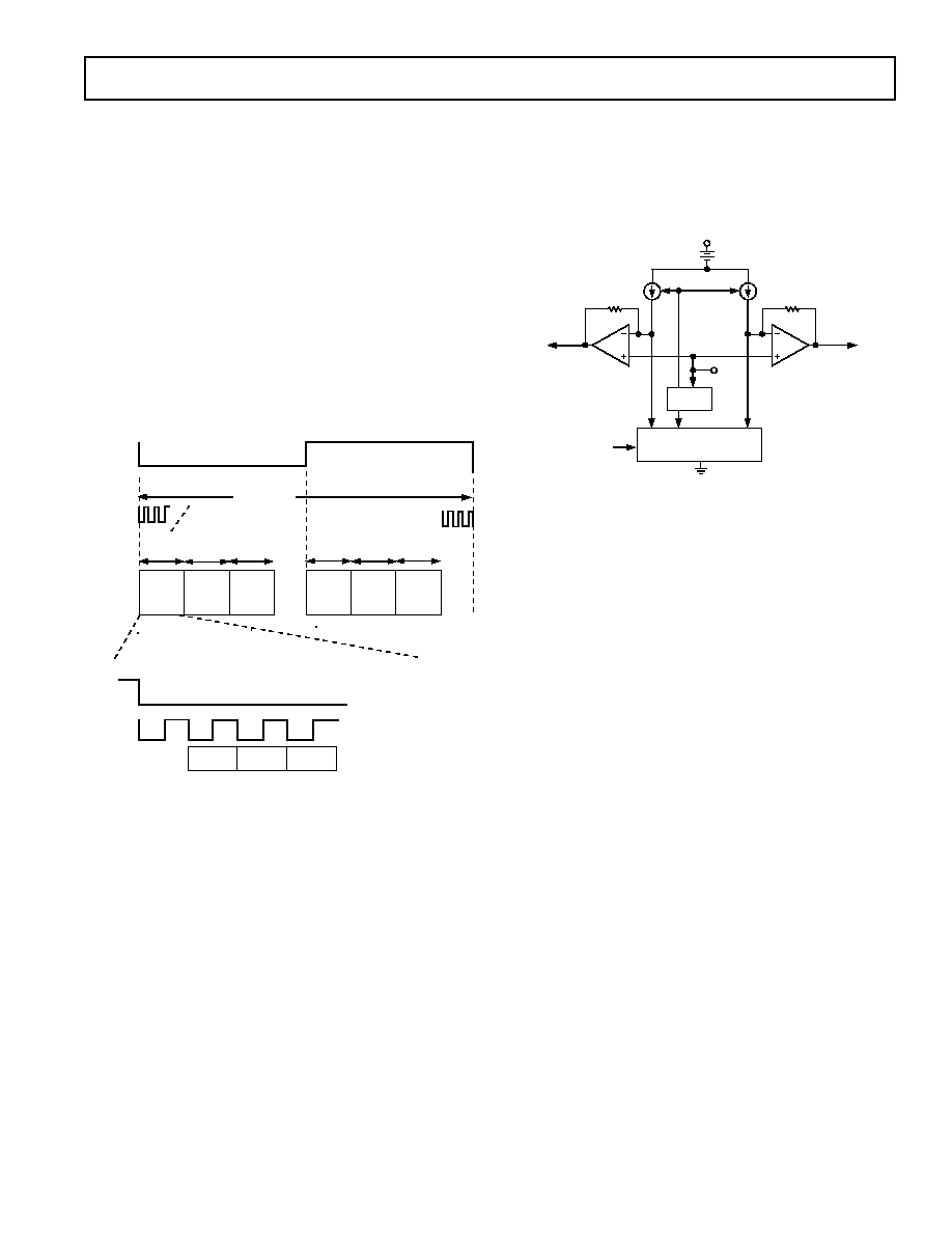
REV. 0
AD1953
≠31≠
For the DSP serial port mode, LRCLK must pulse high for at
least one bit clock period before the MSB of the left channel is
valid, and LRCLK must pulse HIGH again for at least one bit
clock period before the MSB of the right channel is valid. Data
is sampled on the falling edge of BCLK. The DSP serial port
mode can be used with any word length up to 24 bits. In this
mode, it is the responsibility of the DSP to ensure that the left
data is transmitted with the first LRCLK pulse, and that syn-
chronism is maintained from that point forward.
The TDM data capture output mode is shown in Figure 20.
Using this mode allows six channels of serial data to be sent to
an external DAC, allowing the potential for nine total audio
channels. The frame clock is low for the first 128 BCLKs (the
first three data channels), and is then high for the final 128
BCLKs. Each data slot, which is 32 BCLK periods wide, con-
tains one data-word in an I
2
S-like format, with the MSB delayed
by one BCLK period. In this format, data is valid on the rising
edge of the BCLK.
BMUXO/
TDMBC
DMUXO/
TDMO
256BCLKs
32BCLKs 32BCLKs 32BCLKs
32BCLKs
32BCLKs 32BCLKs
LRCLK
BCLK
DATA
SLOT 0
SLOT 1
SLOT 2
SLOT 3
SLOT 4
SLOT 5
MSB
MSB-1
MSB-2
LRMUXO/
TDMFS
Figure 20. TDM Data Capture Output Format
DIGITAL CONTROL PIN
Mute
The AD1953 offers two methods of muting the analog output.
By asserting the MUTE signal high, the left, right, and sub
channels are muted. As an alternative, the user can assert the
mute bit in the serial control register high. The AD1953 has
been designed to minimize pops and clicks when muting and
unmuting the device by automatically ramping the gain up or
down. When the device is unmuted, the volume returns to the
value set in the volume register.
ANALOG OUTPUT SECTION
Figure 21 shows the block diagram of the analog output section.
A series of current sources is controlled by a digital
- modulator.
Depending on the digital code from the modulator, each current
source is connected to the summing junction of either a positive
I-to-V converter or a negative I-to-V converter. Two extra current
sources that push instead of pull are added to set the midscale
common-mode voltage.
All current sources are derived from the VREF input pin. The
gain of the AD1953 is directly proportional to the magnitude of
the current sources, and therefore the gain of the AD1953 is
proportional to the voltage on the VREF pin. With VREF set to
2.5 V, the gain of the AD1953 is set to provide signal swings of
2 V rms differential (1 V rms from each pin). This is the recom-
mended operating condition.
SWITCHED CURRENT
SOURCES
OUT+
OUT≠
I
REF
I
REF
≠ DIG_IN
I
REF
+ DIG_IN
VREF
IN
FROM DIGITAL
- MODULA-
TOR (DIG_IN)
BIAS
I
REF
Figure 21. Internal DAC Analog Architecture
When the AD1953 is used to drive an audio power amplifier
and the compression feature is being used, the VREF voltage
should be derived by dividing down the supply of the amplifier.
This sets a fixed relationship between the digital signal level
(which is the only information available to the digital compressor)
and the full-scale output of the amplifier (just prior to the onset
of clipping). For example, if the amplifier power supply drops
by 10%, the VREF input to the amplifier will also drop by 10%,
which will reduce the analog output signal swing by 10%. The
compressor will therefore be effective in preventing clipping
regardless of any variation in amplifier supply voltage.
Since the VREF input effectively multiplies the signal, care must
be taken to ensure that no ac signals appear on this pin. This
can be accomplished by using a large decoupling capacitor in
the VREF external resistive divider circuit. If the VREF signal is
derived by dividing the 5 V analog supply, the time constant of
the divider must effectively filter any noise on the supply. If the
VREF signal is derived from an unregulated power-amplifier
supply, the time constant must be longer, as the ripple on the
amplifier supply voltage will presumably be greater than in the
case of the 5 V supply.
The AD1953 should be used with an external third-order filter
on each output channel. The circuits shown in Figures 22, 23,
and 24 combine a third-order filter and a single-ended-to-
differential converter in the same circuit. The values used in the
main channel (Figure 22) are for a 100 kHz Bessel filter, and
those used in the subwoofer channel (Figure 23) result in a
10 kHz Bessel filter. The lower frequency filter is used on the
subwoofer output because there is no digital interpolation filter
used in the subwoofer signal path. When calculating the resistor
values for the filter, it is important to take into account the
output resistance of the AD1953, which is nominally 60
.
For best distortion performance, 1% resistors should be used.
The reason for this is that the single-ended performance of the
AD1953 is about 80 dB. The degree to which the single-ended
distortion cancels in the final output is determined by the com-
mon-mode rejection of the external analog filter, which in turn
depends on the tolerance of the components used in the filter.
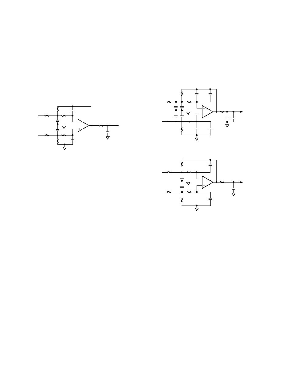
REV. 0
AD1953
≠32≠
The sub output of the AD1953 has a lower drive strength than
the left and right output pins (
±0.25 mA peak versus ±0.5 mA
peak for the left and right outputs). For this reason, it is best to
use higher resistor values in the external sub filter. Figure 24
shows a recommended filter design for the subwoofer output
pins used as a full-bandwidth channel in a custom-designed
program. This design is also a 100 kHz Bessel filter.
For best performance, a large (> 10
µF) capacitor should be
connected between the FILTCAP pin and analog ground. This
pin is connected to an internal node in the bias generator, and
by adding an external capacitance to this pin, the thermal noise
of the left/right channels is minimized. The sub channel is not
affected by this connection.
1.50k
3.01k
2.80k
2.7nF
499
1.00k
806
1nF
820pF
270pF
2.2nF
549
≠ INPUT
+ INPUT
OUT
Figure 22. Recommended External Analog Filter for
Main Channels
GRAPHICAL CUSTOM PROGRAMMING TOOLS
Custom programming tools are available for the AD1953 from
ADI. These graphical tools allow the user to modify the default
signal processing flow by individually placing each block (e.g.,
biquad filter, Phat Stereo, dynamics processor) and connecting
them in any desired fashion. The program then creates a file
that is loaded into the AD1953's program RAM. All of the
contents of the parameter RAM can also be set using these
tools. For more information on these programming tools, email
SigmaDSP@analog.com.
3.01k
11k
11k
56nF
1.5k
5.62k
5.62k
27nF
15nF
6.8nF
220nF
604
≠ INPUT
+ INPUT
OUT
560nF
270nF
68pF
150pF
2.2nF
Figure 23. Recommended External Analog Filter for
Sub Channel
3.01k
11k
11k
56nF
1.5k
5.62k
5.62k
27nF
604
≠ INPUT
+ INPUT
OUT
68pF
150pF
2.2nF
Figure 24. Recommended External Analog Filter for Full
Bandwidth Signals on the Sub Channel Output

REV. 0
AD1953
≠33≠
APPENDIX
Cookbook Formulae for Audio EQ Biquad Coefficients
(adapted from Robert Bristow-Johnson's Internet posting)
For designing a Parametric EQ, follow the steps below.
1. Given:
Frequency
Q
dB_Gain
sample_rate
2. Compute Intermediate Variables
A = 10^(dB_Gain/40)
omega = 2
◊
◊
Frequency/Sample_Rate
sn = sin(omega)
cs = cos(omega)
alpha = sn/(2
◊
Q)
3. Compute Coefficients
b0 = (1 + A
◊
alpha)/(1 + (alpha/A))
b1 = ≠2
◊
cs/(1 + (alpha/A))
b2 = (1 ≠ (alpha/A))/(1 + (alpha/A))
a1 = 2
◊
cs/(1 + (alpha/A)) = ≠b1
a2 = ≠(1 ≠ (alpha/A))/(1 + (alpha/A))
4. The transfer function implemented by the AD1953 is given by:
H(Z) = (b0 + b1
◊
Z
≠1
+ b2
◊
Z
≠2
)/(1 ≠ a1
◊
Z
≠1
≠ a2
◊
Z
≠2
)
Note the inversion in sign of a1 and a2 relative to the more standard form. This form is used in this document because the AD1953
implements the difference equation using the formula below.
Y(n) = a1
◊
y(n ≠ 1) + a2
◊
y(n ≠ 2) + b0
◊
x(n) + b1
◊
x(n ≠ 1) + b2
◊
x(n ≠ 2)

REV. 0
AD1953
≠34≠
OUTLINE DIMENSIONS
48-Lead Low Profile Quad Flat Package [LQFP]
(ST-48)
Dimensions shown in millimeters
TOP VIEW
(PINS DOWN)
1
12
13
25
24
36
37
48
0.27
0.22
0.17
0.50
BSC
7.00
BSC SQ
SEATING
PLANE
1.60
MAX
0.75
0.60
0.45
VIEW A
9.00 BSC
SQ
PIN 1
0.20
0.09
1.45
1.40
1.35
0.10 MAX
COPLANARITY
VIEW A
ROTATED 90 CCW
SEATING
PLANE
10
6
2
7
3.5
0
0.15
0.05
COMPLIANT TO JEDEC STANDARDS MS-026BBC

≠35≠

≠36≠
C02909≠0≠4/03(0)