 | –≠–ª–µ–∫—Ç—Ä–æ–Ω–Ω—ã–π –∫–æ–º–ø–æ–Ω–µ–Ω—Ç: AD1958YRS | –°–∫–∞—á–∞—Ç—å:  PDF PDF  ZIP ZIP |
Document Outline
- Specifications
- Pinout
- Package drawings
- Ordering Guide
- Features
- Applications
- Absolute Maximum Ratings
- Pin Function Description
- PRODUCT OVERVIEW
- TEST CONDITIONS UNLESS OTHERWISE NOTED
- ANALOG PERFORMANCE
- DIGITAL I/O
- TEMPERATURE RANGE
- POWER
- DIGITAL FILTER CHARACTERISTICS
- GROUP DELAY
- CAUTION
- FUNCTIONAL DESCRIPTION
- RESET/POWER-DOWN
- SERIAL CONTROL PORT
- POWER SUPPLY AND VOLTAGE REFERENCE
- SERIAL DATA PORTS€DATA FORMAT
- DIAGRAMS
- Stereo Serial Modes
- Format of SPI Signal
REV. 0
Information furnished by Analog Devices is believed to be accurate and
reliable. However, no responsibility is assumed by Analog Devices for its
use, nor for any infringements of patents or other rights of third parties that
may result from its use. No license is granted by implication or otherwise
under any patent or patent rights of Analog Devices.
a
AD1958
One Technology Way, P.O. Box 9106, Norwood, MA 02062-9106, U.S.A.
Tel: 781/329-4700
www.analog.com
Fax: 781/326-8703
© Analog Devices, Inc., 2001
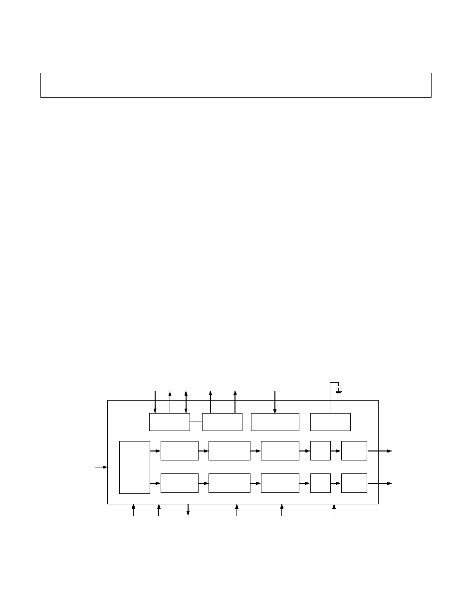
PLL/Multibit - DAC
FUNCTIONAL BLOCK DIAGRAM
OSC
PLL
CIRCUIT
SERIAL CONTROL
INTERFACE
VOLTAGE
REFERENCE
MCLK
AD1958
XIN
LOOP
FILTERS
CLOCK
OUTPUTS
CONTROL DATA
INPUT
MULTIBIT
SIGMA-DELTA
MODULATOR
INTERPOLATOR
8
f
S
ATTEN/MUTE
DAC
OUTPUT
BUFFER
SERIAL
DATA
INTERFACE
MULTIBIT
SIGMA-DELTA
MODULATOR
ATTEN/MUTE
DAC
OUTPUT
BUFFER
16-/20-/24-
BIT DIGITAL
DATA INPUT
3
L
R
ANALOG
OUTPUTS
RESET
MUTE
ZERO FLAG
PLL SUPPLY
DIGITAL SUPPLY
ANALOG SUPPLY
3
2
2
3
2
3
INTERPOLATOR
8
f
S
XOUT
FEATURES
5 V Stereo Audio DAC System
Accepts 16-/18-/20-/24-Bit Data
Supports 24 Bits, 192 kHz Sample Rate
Accepts a Wide Range of Sample Rates Including:
32 kHz, 44.1 kHz, 48 kHz, 88.2 kHz, 96 kHz, and 192 kHz
Multibit Sigma-Delta Modulator with "Perfect Differential
Linearity Restoration" for Reduced Idle Tones and
Noise Floor
Data Directed Scrambling DAC--Least Sensitive to Jitter
Single-Ended Output for Easy Use
108 dB Signal-to-Noise (Not Muted) at 48 kHz Sample
Rate (A-Weighted Stereo)
109 dB Dynamic Range (Not Muted) at 48 kHz Sample
Rate (A-Weighted Stereo)
≠96 dB THD + N (Stereo)
75 dB Stop Band Attenuation
On-Chip Clickless Volume Control
Hardware and Software Controllable Clickless Mute
Serial (SPI) Control for: Serial Mode, Number of Bits,
Sample Rate, Volume, Mute, De-Emphasis
Digital De-Emphasis Processing for 32 kHz, 44.1 kHz,
and 48 kHz Sample Rates
Programmable Dual Fractional-N PLL Clock Generator
27 MHz Master Clock Oscillator
Better than 100 ps rms Master Clock Jitter
Generated System Clocks
SCLK0: 33.8688 MHz
SCLK1: 22.5792 MHz, 24.576 MHz, 33.8688 MHz, or
36.864 MHz
SCLK2: 16.9344 MHz
Flexible Serial Data Port with Right-Justified, Left-
Justified, I
2
S-Compatible, and DSP Serial Port Modes
28-Lead SSOP Plastic Package
APPLICATIONS
DVD, CD, Home Theater Systems, Automotive Audio
Systems, Sampling Musical Keyboards, Digital Mixing
Consoles, Digital Audio Effects Processors
PRODUCT OVERVIEW
The AD1958 is a complete high-performance single-chip stereo
digital audio playback system. It is comprised of a multibit sigma-
delta modulator, digital interpolation filters, and analog output
drive circuitry with an on-board dual PLL clock generator.
Other features include an on-chip stereo attenuator and mute,
programmed through an SPI-compatible serial control port.
The AD1958 is fully compatible with all known DVD formats
including 96 kHz and 192 kHz sample frequencies and 24 bits.
It also is backwards-compatible by supporting 50
µs/15 µs
digital de-emphasis for "redbook" compact discs, as well as
de-emphasis at 32 kHz and 48 kHz sample rates.
The AD1958 has a simple but flexible serial data input port that
allows for glueless interconnection to a variety of ADCs, DSP
chips, AES/EBU receivers, and sample rate converters. The
AD1958 can be configured in left-justified, I
2
S, right-justified,
or DSP serial-port-compatible modes. It can support 16, 20,
and 24 bits in all modes. The AD1958 accepts serial audio data
in MSB first, two's-complement format, and operates from a
single 5 V power supply. It is fabricated on a single monolithic
integrated circuit and housed in a 28-lead SSOP package for
operation over the temperature range ≠40
∞C to +105∞C.

REV. 0
≠2≠
AD1958≠SPECIFICATIONS
TEST CONDITIONS UNLESS OTHERWISE NOTED
Supply Voltages
(AVDD, DVDD, PVDD)
5.0 V
Ambient Temperature
25
∞C
Input Clock
12.288 MHz (256
◊ f
S
Mode)
Input Signal
996.0938 Hz,
0 dB Full Scale
Input Sample Rate
48 kHz
Measurement Bandwidth
20 Hz to 20 kHz
Word Width
24 Bits
Load Capacitance
100 pF
Load Impedance
47 k
Input Voltage HI
2.0 V
Input Voltage LO
0.8 V
ANALOG PERFORMANCE
Min
Typ
Max
Unit
Resolution
24
Bits
Signal-to-Noise Ratio (20 Hz to 20 kHz)
No Filter (Stereo)
105
dB
With A-Weighted Filter (Stereo)
108
dB
Dynamic Range (20 Hz to 20 kHz, ≠60 dB Input)
No Filter (Stereo)
105
dB
With A-Weighted Filter (Stereo)
102
109
dB
Total Harmonic Distortion + Noise (Stereo)
≠90
≠96
dB
PLL Performance
Master Clock Input Frequency
27
MHz
Generated System Clocks
SCLK0
33.8688
MHz
SCLK1
12.288
MHz
SCLK2
22.5792
MHz
Jitter (SCLK0 and SCLK1)
110
175
ps rms
Jitter (MCLK)
60
100
ps rms
Duty Cycle (SCLK0, SCLK1)
1
50
%
Duty Cycle (MCLK)
49
50
51
%
Analog Outputs
Single-Ended Output Range (
±Full Scale)
3.17
V p-p
Output Capacitance at Each Output Pin
2
pF
Out-of-Band Energy (0.5
◊ f
S
to 100 kHz)
≠90
dB
V
REF
(FILTR)
2.39
V
DC Accuracy
Gain Error
≠5
±2.0
+5
%
Interchannel Gain Mismatch
≠0.15
±0.015
+0.15
dB
Gain Drift
150
250
ppm/
∞C
DC Offset
≠25
≠3
+20
mV
Interchannel Crosstalk (EIAJ Method)
≠120
dB
Interchannel Phase Deviation
±0.1
Degrees
Mute Attenuation
≠100
dB
De-Emphasis Gain Error
±0.1
dB
NOTES
1
In some combinations with Clock Configuration Mode = 1 (see Table III), SCLK will not be 50%.
2
Performance of right and left channels is identical (exclusive of the Interchannel Gain Mismatch and Interchannel Phase Deviation specifications).
Specifications subject to change without notice.
DIGITAL I/O (≠40
∞C to +105∞C )
Min
Typ
Max
Unit
Input Voltage HI (V
IH
)
2.0
V
Input Voltage LO (V
IL
)
0.8
V
Input Leakage (I
IH
@ V
IH
= 2.4 V)
10
µA
Input Leakage (I
IL
@ V
IL
= 0.8 V)
10
µA
High Level Output Voltage (V
OH
) I
OH
= 1 mA
3.5
V
Low Level Output Voltage (V
OL
) I
OL
= 1 mA
0.4
V
Input Capacitance
20
pF
Specifications subject to change without notice.

REV. 0
≠3≠
AD1958
TEMPERATURE RANGE
Min
Typ
Max
Unit
Specifications Guaranteed
25
∞C
Functionality Guaranteed
≠40
+105
*
∞C
Storage
≠55
+125
∞C
NOTE
*105
∞C ambient guaranteed for a 4-layer board, two 1 oz. planes, two 2 oz. signal layers. Derate to 85∞C for 2-layer board, 2 oz. layers.
Specifications subject to change without notice.
POWER
Min
Typ
Max
Unit
Supplies
Voltage, Analog Digital PLL
4.50
5
5.50
V
Analog Current
36
41
mA
Digital Current
25
29
mA
PLL Current
30
34
mA
Dissipation
Operation--All Supplies
455
540
mW
Operation--Analog Supply
180
mW
Operation--Digital Supply
125
mW
Operation--PLL Supply
150
mW
Power Supply Rejection Ratio
1 kHz 300 mV p-p Signal at Analog Supply Pins
≠60
dB
20 kHz 300 mV p-p Signal at Analog Supply Pins
≠50
dB
Specifications subject to change without notice.
DIGITAL FILTER CHARACTERISTICS
Sample Rate (kHz)
Pass Band (kHz)
Stop Band (kHz)
Stop Band Attenuation (dB)
Pass Band Ripple (dB)
44.1
DC≠20
24.1≠328.7
75
±0.0002
48
DC≠21.8
26.23≠358.28
75
±0.0002
96
DC≠39.95
56.9≠327.65
75
±0.0005
192
DC≠87.2
117≠327.65
60
0/≠0.04 (DC≠21.8 kHz)
0/≠0.5 (DC≠65.4 kHz)
0/≠1.5 (DC≠87.2 kHz)
Specifications subject to change without notice.
GROUP DELAY
Chip Mode
Group Delay Calculation
f
S
Group Delay
Unit
INT8
◊ Mode
24.625/f
S
48 kHz
513
µs
INT4
◊ Mode
15.75/f
S
96 kHz
164
µs
INT2
◊ Mode
14/f
S
192 kHz
72.91
µs
Specifications subject to change without notice.
DIGITAL TIMING (Guaranteed over ≠40
∞C to +105 C, AVDD = DVDD = PVDD = 5.0 V 10%)
Min
Unit
t
DMP
MCLK Period (FMCLK = 256
◊ FLRCLK)
54
ns
t
DML
MCLK LO Pulsewidth (All Modes)
15
ns
t
DMH
MCLK HI Pulsewidth (All Modes)
10
ns
t
DBH
BCLK HI Pulsewidth
20
ns
t
DBL
BCLK LO Pulsewidth
20
ns
t
DBP
BCLK Period
60
ns
t
DLS
LRCLK Setup
20
ns
t
DLH
LRCLK Hold (DSP Serial Port Mode Only)
20
ns
t
DDS
SDATA Setup
15
ns
t
DDH
SDATA Hold
15
ns
t
RSTL
RST LO Pulsewidth
15
ns
Specifications subject to change without notice.
REV. 0
AD1958
≠4≠
ABSOLUTE MAXIMUM RATINGS
*
DVDD to DGND . . . . . . . . . . . . . . . . . . . . . . ≠0.3 V to +6 V
AVDD to DGND . . . . . . . . . . . . . . . . . . . . . . ≠0.3 V to +6 V
Digital Inputs . . . . . . . . . . DGND ≠ 0.3 V to DVDD + 0.3 V
Analog Inputs . . . . . . . . . . AGND ≠ 0.3 V to AVDD + 0.3 V
AGND to DGND . . . . . . . . . . . . . . . . . . . . ≠0.3 V to + 0.3 V
Reference Voltage . . . . . . . . . . . . . . . . . . . . . (AVDD + 0.3)/2
Soldering (10 sec) . . . . . . . . . . . . . . . . . . . . . . . . . . . . . 300
∞C
*Stresses above those listed under Absolute Maximum Ratings may cause perma-
nent damage to the device. This is a stress rating only; functional operation of the
device at these or any other conditions above those listed in the operational
sections of this specification is not implied. Exposure to absolute maximum rating
conditions for extended periods may affect device reliability. Only one absolute
maximum rating may be applied at any one time.
PACKAGE CHARACTERISTICS
Min
Typ
Max
Unit
JA
(Thermal Resistance)
109.0
∞C/W
Junction-to-Ambient
(2-Layer Board)
JA
(Thermal Resistance)
78.58
∞C/W
Junction-to-Ambient
(4-Layer Board--
2 Signal, 2 Planes)
JA
(Thermal Resistance)
Junction-to-Case
39.0
∞C/W
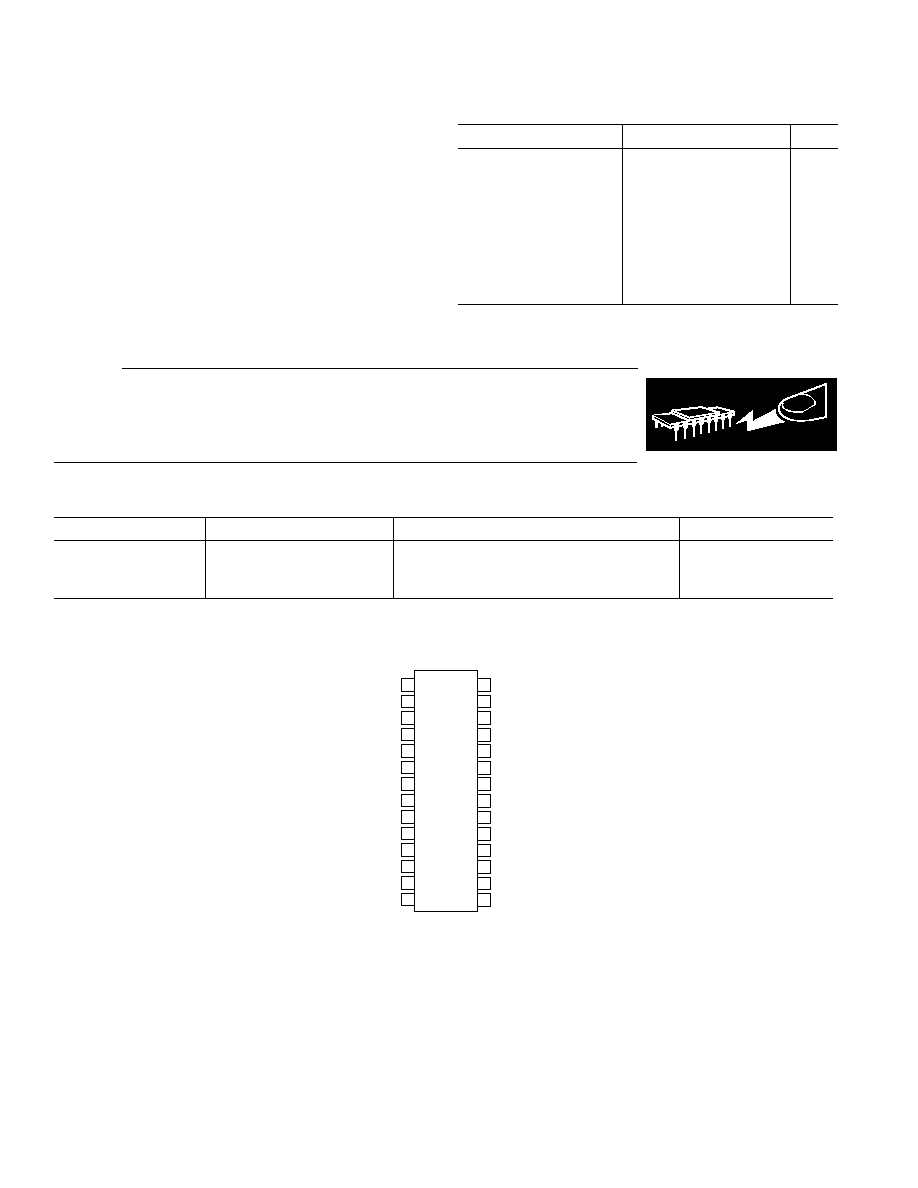
PIN CONFIGURATION
TOP VIEW
(Not to Scale)
28
27
26
25
24
23
22
21
20
19
18
17
16
15
1
2
3
4
5
6
7
8
9
10
11
12
13
14
AD1958
XIN
XOUT
MCLK
SCLK2
SCLK1
SCLK0
DGND
CCLK
CLATCH
RESET
LRCLK
DVDD
SDATA
BCLK
PVDD
PGND
LF0
LF1
AGND0
OUTR
FLTR
CDATA
MUTE
ZERO
FILTB
AGND1
OUTL
AVDD
CAUTION
ESD (electrostatic discharge) sensitive device. Electrostatic charges as high as 4000 V readily
accumulate on the human body and test equipment and can discharge without detection. Although
the AD1958 features proprietary ESD protection circuitry, permanent damage may occur on
devices subjected to high-energy electrostatic discharges. Therefore, proper ESD precautions are
recommended to avoid performance degradation or loss of functionality.
WARNING!
ESD SENSITIVE DEVICE
ORDERING GUIDE
Model
Temperature
Package Description
Package Option
AD1958YRS
≠40
∞C to +105
∞C
28-Lead Small Outline Package
RS-28
AD1958YRSRL
≠40
∞C to +105
∞C
28-Lead Small Outline Package
RS-28 on 13" Reels
EVAL-AD1958EB
Evaluation Board

REV. 0
AD1958
≠5≠
PIN FUNCTION DESCRIPTIONS
Pin
Input/Output
Mnemonic
Description
1
I
CCLK
Control Clock Input for Control Data. Control input data must be valid on
the rising edge of CCLK. CCLK may be continuous or gated.
2
I
CLATCH
Latch Input for Control Data
3
I
RESET
Reset. The AD1958 is placed in a reset mode when this pin is held LO.
The serial control port registers are reset to their default values. Set HI for
normal operation.
4
I
LRCLK
Left/Right Clock Input for Input Data. Must run continuously.
5
I
BCLK
Bit Clock Input for Input Data. Need not run continuously; may be gated
or used in a burst fashion.
6
I
SDATA
Serial input, MSB first, containing two channels of 16/20/24 bits of two's-
complement data per channel.
7
I
DVDD
Digital Power Supply Connect to Digital 5 V Supply
8
I
DGND
Digital Ground
9
O
SCLK0
33.8688 MHz Clock Output
10
O
SCLK1
256/384/512/768 f
S
Output
11
O
SCLK2
16.9344 MHz/22.5792 MHz/512 f
S
Output
12
I/O
MCLK
27 MHz Master Clock Output/256 f
S
DAC Clock Input
13
O
XOUT
27 MHz Crystal Oscillator Output
14
I
XIN
27 MHz Crystal Oscillator/External Clock Input
15
PVDD
PLL Power Supply. Connect to PLL 5 V Supply.
16
PGND
PLL Ground
17
LF0
PLL0 Loop Filter
18
LF1
PLL1 Loop Filter
19
AGND0
Analog Ground
20
O
OUTR
Right Channel Positive Line Level Analog Output
21
O
FILTR
Voltage Reference Filter Capacitor Connection. Bypass and decouple the
voltage reference with parallel 10
µF and 0.1 µF capacitors to AGND.
22
I
AGND1
Analog Ground
23
O
OUTL
Left Channel Line Level Analog Output
24
AVDD
Analog Power Supply. Connect to Analog 5 V Supply.
25
FILTB
Filter Capacitor Connection. Connect 10
µF Capacitor to AGND.
26
O
ZERO
Zero Flag Output. This pin goes HI when both channels have zero signal
input for more than 1024 L/R Clock Cycles.
27
I
MUTE
Mute. Assert HI to Mute Both Stereo Analog Outputs. Deassert LO for
normal operation.
28
I
CDATA
Serial Control Input, MSB first, containing 16 bits of unsigned data
per channel. Used for specifying channel-specific attenuation and mute.
FUNCTIONAL DESCRIPTION
DAC
The AD1958 has two DAC channels arranged as a stereo pair
with single-ended analog outputs. Each channel has its own
independently programmable attenuator, adjustable in 16384
linear steps. Digital inputs are supplied through a serial data
input pin, SDATA, a frame clock, LRCLK, and a bit clock, BLCK.
Each analog output pin sits at a dc level of V
REF
(present at
FILTR), and swings
± 1.585 V for a 0 dB digital input signal.
A single op amp third-order external low-pass filter is recom-
mended to remove high-frequency noise present on the output
pins. The output phase can be changed in an SPI control
register to accommodate inverting and noninverting filters.
Note that the use of op amps with low slew rate or low band-
width may cause high frequency noise and tones to fold down
into the audio band; care should be exercised in selecting
these components.
The FILTB and FILTR pins should be bypassed by external
capacitors to ground. The FILTB pin is used to reduce the noise
of the internal DAC bias circuitry, thereby reducing the DAC
output noise. The voltage at the V
REF
pin, FILTR (V
REF
~ 2.39 V)
can be used to bias external op amps used to filter the output signals.
The DAC master clock frequency is 256 f
S
for the 32 kHz≠48 kHz
range (8 interpolation, see Table I). For the 96 kHz range (4
interpolation) this is 128 f
S
. At 192 kHz (2 interpolation), this
is 64 f
S
. It is supplied internally from the PLL clock system when
MCLK mode is set to Output in the PLL Control Register.
When the MCLK mode is changed to Input, it must be supplied
from an external source connected to MCLK. The output from
the 27 MHz PLL clock is disabled in this case.
REV. 0
AD1958
≠6≠
Table I. DAC Control Register
Bit 11:10
Bit 9:8
Bit 7
Bit 6
Bit 5:4
Bit 3:2
Bit 1:0
Interpolation
Serial Data
Serial Data
De-Emphasis
SPI Register
Factor
Width
Output Phase
Soft Mute
Format
Filter
Address
00 = 8
◊*
00 = 24 Bits
*
0 = Noninverted
*
0 = No Mute
*
00 = I
2
S
*
00 = None
*
01
01 = 4
◊
01 = 20 Bits
1 = Inverted
1 = Muted
00 = Right Justified
01 = 44.1 kHz
10 = 2
◊
10 = 16 Bits
10 = DSP
10 = 32 kHz
11 = Not Allowed
11 = 16 Bits
11 = Left Justified
11 = 48 kH
z
*Default Setting
Table III. PLL Control Register
Bit 11
Bit 10
Bit 9
Bit 8
Bit 7:6
Bit 5
Bit 4
Bit 3
Bit 2
Bit 1:0
PLL2
PLL1
XTAL
SPI
Power-
Power-
Power-
Clock
SCLK1
Frequency
SCLK2
MCLK
Register
Down
Down
Down
Configuration
f
S
Select
Double
2
Select
Mode
Address
0 = On
1
0 = On
1
0 = On
1
0 = Mode 0
1
SCLK1 =
Reserved
Reserved
0 = Output
1
11
1 = PD
1 = PD
1 = PD
000: 36.864 MHz
1
Set to 0
Set to 0
1 = Input
100: 24.576 MHz
110: 33.8688 MHz
111: 22.5792 MHz
Other combinations reserved
SCLK2 = 16.9344 MHz
1 = Mode 1
00 = 48 kHz
0 = 256 f
S
0 = Normal
0 = 22.5792 MHz
01 = Not
1 = 384 f
S
1 =
1 = 512 f
S
2
Allowed
f
NOMINAL
2
10 = 32 kHz
11 = 44.1 kHz
NOTES
1
Default Setting
2
In Mode 1, Frequency Double affects SCLK1 always and SCLK2 in 512 f
S
mode.
PLL CLOCK SYSTEM
The PLL clock system is expected to be run from a 27 MHz
master clock supplied by the on-board crystal oscillator or an
external source connected to XIN. With the MCLK mode set
to Output, the 27 MHz clock is buffered out to the MCLK
pin. When set to Input, this pin is the 256 f
S
master clock input
for the DAC. SCLK0 is always set to 33.8688 MHz. SCLK1 is
intended to be used as a master audio clock and will be a multiple
of the sample rate set in the PLL control register (see Table III).
In Mode 0 (Bit 8), it can be set to 512 or 768 times either
44.1 kHz or 48 kHz. SCLK2 will be 16.3944 MHz (384
44.1 kHz). In Mode 1, SCLK1 can be set to 256, 384, 512,
or 768 times 32 kHz, 44.1 kHz, or 48 kHz. SCLK2 can be
set to a constant 22.5792 MHz (512 44.1 kHz) or 512 f
S
.
There are two loop filter pins, LF0 and LF1. They should each
be bypassed to PVDD by a network consisting of a 33 nF capaci-
tor in series with a 750
resistor, paralleled with a 1.8 nF capacitor.
The 27 MHz Master Clock oscillator should have a crystal cut for
an 18 pF load connected between XIN and XOUT, with 22 pF
capacitors connected from XIN and XOUT to PGND.
Table II. DAC Volume Registers
Bit 15:2
Bit 1:0
Volume
SPI Register Address
14 Bits, Unsigned
00 = Left Volume
14 Bits, Unsigned
10 = Right Volume
Default is full volume
RESET/POWER-DOWN
RESET will set the control registers to their default settings. The
chip should be reset on power-up. After reset is deasserted, the
part will come out of reset on the next rising LRCLK.
SERIAL CONTROL PORT
The AD1958 has an SPI-compatible control port to permit
programming the internal control registers for the PLL and DAC.
The DAC output levels may be independently programmed
by means of an internal digital attenuator adjustable in 16384
linear steps.
REV. 0
AD1958
≠7≠
CLATCH
CCLK
CDATA
D0
D15
D14
Figure 1. Format of SPI Signal
LRCLK
BCLK
SDATA
LEFT CHANNEL
RIGHT CHANNEL
MSB
MSB
MSB
MSB
MSB
MSB
LSB
LSB
LSB
LSB
LSB
MSB
MSB
LSB
LSB
LEFT-JUSTIFIED MODE--16 TO 24 BITS PER CHANNEL
1
2
S MODE--16 TO 24 BITS PER CHANNEL
RIGHT-JUSTIFIED MODE--SELECT NUMBER OF BITS PER CHANNEL
DSP MODE--16 TO 24 BITS PER CHANNEL
1/f
S
NOTES
1. DSP MODE DOES NOT IDENTIFY CHANNEL.
2. LRCLK NORMALLY OPERATES AT f
S
EXCEPT FOR DSP MODE WHICH IS 2
f
S
.
3. BCLK FREQUENCY IS NORMALLY 64
LRCLK BUT MAY BE OPERATED IN BURST MODE.
LRCLK
BCLK
SDATA
LRCLK
BCLK
SDATA
LRCLK
BCLK
SDATA
LEFT CHANNEL
RIGHT CHANNEL
LEFT CHANNEL
RIGHT CHANNEL
LSB
Figure 2. Stereo Serial Modes
The SPI control port is a 3-wire serial control port. The format
is similar to the Motorola SPI format except the input data word
is 16 bits wide. Max serial bit clock frequency is 8 MHz and
may be completely asynchronous to the PLL system or the
DAC. Figure 1 shows the format of the SPI signal. Note that
the CCLK can be gated or continuous,
CLATCH should be
low during the 16 active clocks.
POWER SUPPLY AND VOLTAGE REFERENCE
The AD1958 is designed for five-volt supplies. Separate power
supply pins are provided for the analog, digital, and PLL sec-
tions. These pins should be bypassed with 100 nF ceramic
chip capacitors, as close to the pins as possible, to minimize
noise. A bulk aluminum electrolytic capacitor of at least 22
µF
should also be provided on the same PC board. For best perfor-
mance it is recommended that the analog supply be separate
from the digital and PLL supply. It is recommended that all
supplies be isolated by ferrite beads in series with each supply. It
is expected that the digital and PLL sections will be run from a
common supply but isolated from one another. It is important
that the analog supply be as clean as possible.
The internal voltage reference is brought out on Pin 21 (FILTR)
and should be bypassed as close as possible to the chip with a
parallel combination of 10
µF and 100 nF. The reference volt-
age may be used to bias external op amps to the common-mode
voltage of the analog output signal pins. The current drawn
from the FILTR pin should be limited to less than 50
µA.
SERIAL DATA PORTS--DATA FORMAT
The DAC serial data input mode defaults to I
2
S. By changing
Bits 4 and 5 in the DAC control register, the mode can be
changed to RJ, DSP, or LJ. The word width defaults to 24 bits
but can be changed by programming Bits 8 and 9 in the DAC
Control Register.
Figure 2 shows the serial mode formats.

REV. 0
≠8≠
C02708≠0≠10/01(0)
PRINTED IN U.S.A.
AD1958
28-Lead Small Outline Package (SSOP)
(RS-28)
0.009 (0.229)
0.005 (0.127)
0.03 (0.762)
0.022 (0.558)
8
0
0.008 (0.203)
0.002 (0.050)
0.07 (1.79)
0.066 (1.67)
0.078 (1.98)
0.068 (1.73)
0.015 (0.38)
0.010 (0.25)
SEATING
PLANE
0.0256
(0.65)
BSC
0.311 (7.9)
0.301 (7.64)
0.212 (5.38)
0.205 (5.21)
28
15
14
1
0.407 (10.34)
0.397 (10.08)
PIN 1
CONTROLLING DIMENSIONS ARE IN MILLIMETERS; INCH DIMENSIONS
ARE ROUNDED-OFF MILLIMETER EQUIVALENTS FOR REFERENCE
ONLY AND ARE NOT APPROPRIATE FOR USE IN DESIGN
OUTLINE DIMENSIONS
Dimensions shown in inches and (mm).