 | –≠–ª–µ–∫—Ç—Ä–æ–Ω–Ω—ã–π –∫–æ–º–ø–æ–Ω–µ–Ω—Ç: AD1983 | –°–∫–∞—á–∞—Ç—å:  PDF PDF  ZIP ZIP |
Document Outline
- ˛ˇ
- ˛ˇ
- ˛ˇ
- ˛ˇ
- ˛ˇ
- ˛ˇ
- ˛ˇ
- ˛ˇ
- ˛ˇ
- ˛ˇ
- ˛ˇ
HD Audio SoundMAX
Æ
Codec
AD1983
Rev. 0
Information furnished by Analog Devices is believed to be accurate and reliable. However, no
responsibility is assumed by Analog Devices for its use, nor for any infringements of patents or other
rights of third parties that may result from its use. Specifications subject to change without notice. No
license is granted by implication or otherwise under any patent or patent rights of Analog Devices.
Trademarks and registered trademarks are the property of their respective owners.
One Technology Way, P.O. Box 9106, Norwood, MA 02062-9106, U.S.A.
Tel: 781.329.4700
www.analog.com
Fax: 781.461.3113
©2006 Analog Devices, Inc. All rights reserved.
FEATURES
2 DAC channels: 16-, 20-, or 24-bit
2 ADC channels: 16- or 20-bit
HD audio sample rates
8 kHz, 11.025 kHz, 16 kHz, 22.05 kHz, 32 kHz,
44.1 kHz, 48 kHz
Greater than 90 dB dynamic range
S/PDIF output: 32 kHz, 44.1 kHz, or 48 kHz, 16- or 24-bit
Digital BEEP generator
Integrated headphone amplifiers
Selectable microphone inputs with preamplifiers
Stereo line level inputs
Full analog mixer
2 GPIOs for external circuit control, jack sense
32-lead, Pb-free LFCSP_VQ (QFN) package
ENHANCED FEATURES
No AFILT pins, results in BOM savings
Jack sensing autoconfiguration options
Mute line output and monaural output (MONO_OUT)
when headphones are used
Mute MONO_OUT when a device is in the line out jack
Selectable sense trip level: high/low supports all jack types
Peripheral identification/enumeration
Jack presence detection: HD Audio SENSE and GPIOs
Microphone to MONO_OUT for speakerphone
Advanced power management modes
2 software-controlled microphone bias pins
Stereo microphone array capture
Source from two different ports
0 dB, 10 dB, 20 dB, and 30 dB boost options
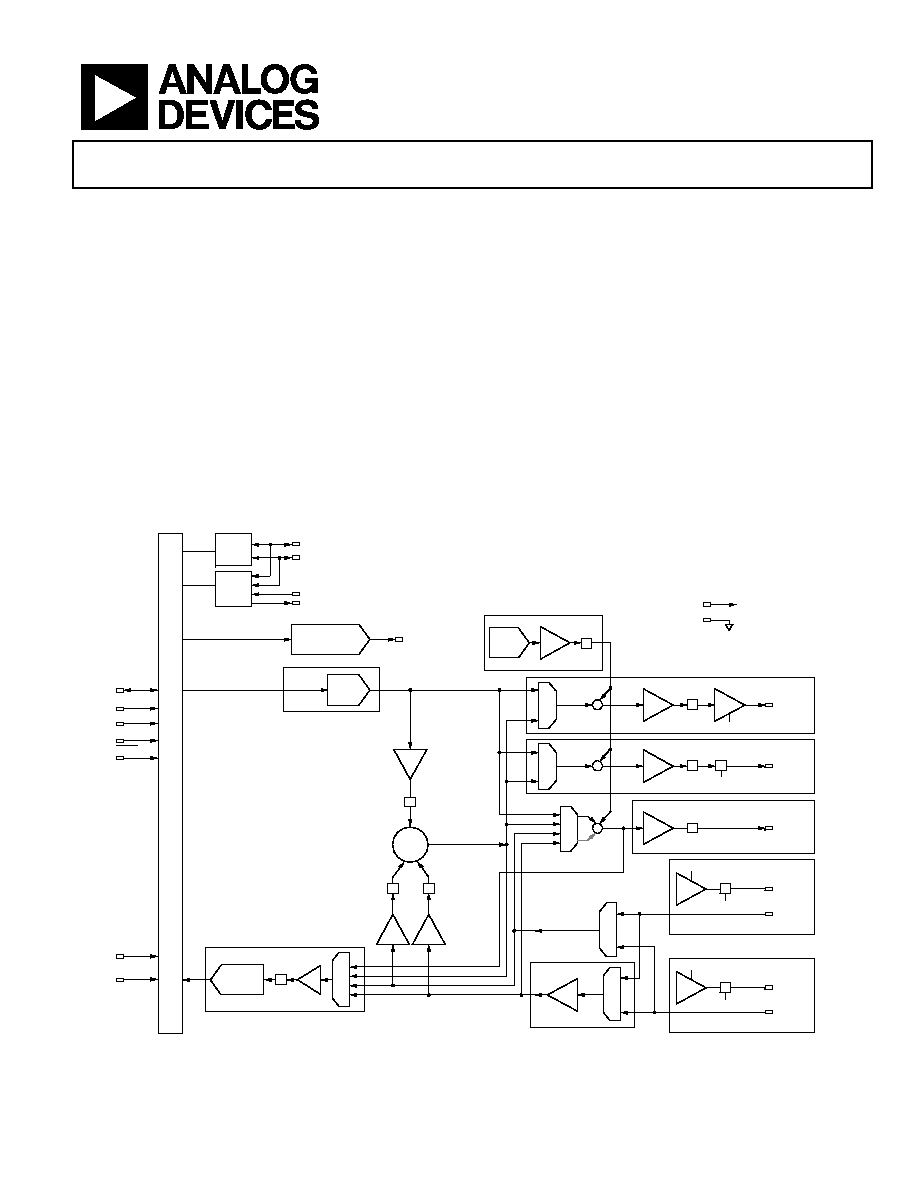
FUNCTIONAL BLOCK DIAGRAM
GPIO_0/JS_1
GPIO_1/JS_0
SENSE_A
S/PDIF_OUT
SENSE_SRC
GPIO
JACK
SENSE
DV
SS
DV
DD
AV
SS
AV
DD
20-BIT
48kHz
PCM/FLOAT32
- ADC
NID: 04
NID: 0C
NID: 0D
SELEC
T
O
R
4:
1
SE
L
E
C
T
O
R
2:
1
SE
L
E
C
T
O
R
4:
1
G
NID: 01
+3.3V
0dB TO +22.5dB
≠34.5dB TO +12dB
SDATA_IN
BIT_CLK
RESET
SYNC
SDATA_OUT
GA
NID: 11
NID: 0E
GA
NID: 12
GA
NID: 13
NID: 09
MIC
BIAS
BIAS_EN
Z
MIC_BIAS-C
PORT-C
LINE IN
NID: 0F
NID: 0B
SELEC
T
O
R
2:
1
GA
M
NID: 07
MONO_OUT
OUTPUT_EN
≠46.5dBTO +3dB
GA
M
NID: 05
PORT-D
FRONT
≠46.5dBTO +3dB
BOOST
0dB, 10dB, 20dB, 30dB
SE
L
E
C
T
O
R
2:
1
NID: 10
DIGITAL
PCBEEP
0dB TO ≠45.0dB
3dB STEPS
G
M
M
M
≠34.5dB TO +12dB
M
≠34.5dB TO +12dB
M
NID: 03
NID: 02
NID: 0A
24-BIT
48kHz
PCM
- DAC
16-, 20-, 24-BIT
32kHz, 44.1kHz, 48kHz
PCM/AC3
S/PDIF TX
Z
SELE
C
T
O
R
2:
1
OUTPUT_EN
GA
M
NID: 06
PORT-A
HEADPHONE
≠46.5dBTO +3dB
+5.0V
HP
NID: 08
MIC
BIAS
BIAS_EN
Z
MIC_BIAS-B
PORT-B
MIC
0
5205-
0
01
HD
AU
DI
O
I
N
T
E
RF
AC
E
BIAS_SEL
BIAS_SEL
Figure 1.

AD1983
Rev. 0 | Page 2 of 16
TABLE OF CONTENTS
Features .............................................................................................. 1
Enhanced Features............................................................................ 1
Functional Block Diagram .............................................................. 1
Revision History ............................................................................... 2
Specifications..................................................................................... 3
Test Conditions............................................................................. 3
Power Down Dissipation............................................................. 5
Absolute Maximum Ratings............................................................ 6
Environmental Conditions ..........................................................6
ESD Caution...................................................................................6
Pin Configuration and Function Descriptions..............................7
HD Audio Codec Information ........................................................9
Verb Support ............................................................................... 12
Jack Presence Detection................................................................. 14
Outline Dimensions ....................................................................... 15
Ordering Guide .......................................................................... 15
REVISION HISTORY
4/06--Revision 0: Initial Version

AD1983
Rev. 0 | Page 3 of 16
SPECIFICATIONS
TEST CONDITIONS
Test conditions for the AD1983 are as follows, unless otherwise noted.
General Test Conditions
Temperature at 25∞C
Digital supply (DV
DD
) at 3.3 V ± 10%
Analog supply (AV
DD
) at 5.0 V ± 10%
Sample rate (F
S
) at 48 kHz
Input signal at 1.0 kHz
Analog output pass band at 20 Hz to 20,000 Hz
V
IH
at 2.0 V
V
IL
at 0.8 V
V
IH
at 2.4 V
V
IL
at 0.6 V
DAC Test Conditions
Calibrated
Output -3 dB relative to full scale
10 k output load, Port D, and MONO_OUT
32 output load, Port A
ADC Test Conditions
Calibrated
0 dB PGA gain
Input -3.0 dB relative to full scale
Table 1.
Parameter
Conditions
Min
Typ
Max
Unit
ANALOG INPUT
Port-B, Port-C
0 dB
1
V rms
1
2.83
V
p-p
Port-B, Port-C
10 dB
0.316
V rms
0.894
V
p-p
Port-B, Port-C
20 dB
0.1
V rms
0.283
V
p-p
Port-B, Port-C
30 dB
0.032
V rms
0.089
V
p-p
Input Impedance
2
20
k
Input Capacitance
2
5
7.5
pF
MASTER VOLUME
Step Size
Port-A, Port-D, MONO_OUT
1.5
dB
Output Gain Range
≠46.5
+3
dB
Mute Attenuation of 0 dB Fundamental
80
dB
PROGRAMMABLE GAIN AMPLIFIER--
ADC
Step Size
1.5
dB
PGA Gain Range
0.0
22.5
dB
ANALOG MIXER--INPUT
GAIN/AMPLIFIERS/ATTENUATORS
Signal-to-Noise Ratio (SNR)
Line In to Line Out
85
dB
Microphone In to Line Out
2
80
dB
Step Size
All mixer inputs except digital PC BEEP
1.5
dB
Step Size: Digital PC Beep
3.0
dB
Input Gain Range
All mixer inputs except digital PC BEEP
-34.5
+12.0
dB
Digital PC Beep
-45.0
0.0
dB
DIGITAL DECIMATION AND
INTERPOLATION FILTERS
2
Pass Band
0
0.4 ◊ F
S
Hz
Pass-Band Ripple
±0.09
dB
Transition Band
0.4 ◊ F
S
0.6 ◊ F
S
Hz
Stop Band
0.6 ◊ F
S
Hz
Stop-Band Rejection
-74
dB

AD1983
Rev. 0 | Page 4 of 16
Parameter
Conditions
Min
Typ
Max
Unit
Group Delay
16/F
S
sec
Group Delay Variation over Pass Band
0
s
ANALOG-TO-DIGITAL CONVERTERS
Resolution
+20
Bits
Total Harmonic Distortion (THD)
-92
dB
Dynamic Range
-60 dB input, THD + N referenced to F
S
,
A-weighted
-85
dB
Crosstalk
2
Line inputs: Input L, Ground R, Read R; Input R,
Ground L, Read L
-80
dB
Line inputs and other inputs
-100
-80
dB
Gain Error
Full-
scale span relative to nominal input voltage
±10
%
Interchannel Gain Mismatch
Difference of gain errors
±0.5
dB
ADC Offset Error
2
±5
mV
DIGITAL-TO-ANALOG CONVERTERS
Resolution
+24
Bits
Total Harmonic Distortion (THD)
Line out
-86
dB
Headphone
out
-76
dB
Dynamic Range
-60 dB input, THD + N referenced to F
S
,
A-weighted
-90
dB
Gain Error
Full-scale span relative to nominal input voltage
±10
%
Interchannel Gain Mismatch
Difference of gain errors
±0.7
dB
DAC Crosstalk
2
Input L, Zero R, Read R out; Input R, Zero L,
Read L out
-80
dB
ANALOG OUTPUT
Full-Scale Output Voltage
Port-D and MONO_OUT
1
V rms
2.83
V
p-p
Output Impedance
2
300
External Load Impedance
2
10
k
Output Capacitance
2
15
pF
External Load Capacitance
1000
pF
Full-Scale Output Voltage
Port-A: headphone out
1
V rms
2.83
V
p-p
External Load Impedance
2
32
Output Capacitance
2
15
pF
External Load Capacitance
2
1000
pF
VREF_FILT
2.050
2.250
2.450
V
MIC_BIAS (Port-B and Port-C)
At 50% setting
2.250
V
At 80% setting
3.700
V
At 0% setting
0.0
V
Current Drive
5
mA
Mute Click
Muted output, unmuted midscale DAC output
±5
mV
STATIC DIGITAL SPECIFICATIONS
High Level Input Voltage (V
IH
), Digital
Inputs
0.65 ◊ DV
DD
V
Low Level Input Voltage (V
IL
)
0.35 ◊ DV
DD
V
High Level Output Voltage (V
OH
) I
OH
= 2 mA
0.90 ◊ DV
DD
V
Low Level Output Voltage (V
OL
) I
OL
= 2 mA
0.10 ◊ DV
DD
V
Input Leakage Current
-10
+10
A
Output Leakage Current
-10
+10
A
Input/Output Pin Capacitance
7.5
pF
AD1983
Rev. 0 | Page 5 of 16
Parameter
Conditions
Min
Typ
Max
Unit
POWER
SUPPLY
Power Supply Range
Analog
(AV
DD
) ±10%
4.5
5.5
V
Digital
(DV
DD
) ±10%
2.97
3.63
V
Power Dissipation--Analog
(AV
DD
)/Digital (DV
DD
)
165/125
mW
Analog Supply Current--Analog
(AV
DD
)
33
mA
Digital Supply Current--Digital
(DV
DD
)
38
mA
Power Supply Rejection
100 mV p-p signal @ 1 kHz
40
dB
1
RMS values assume sine wave input.
2
Guaranteed by design; not production tested.
POWER DOWN DISSIPATION
Table 2.
Parameter
DV
DD
AV
DD
Unit
FUNCTION NODE
1
0
1.8
mA
DAC 30
26
mA
ADC 28
26
mA
MIXER 37
17
mA
1
BIT_CLK off.
AD1983
Rev. 0 | Page 6 of 16
ABSOLUTE MAXIMUM RATINGS
Table 3.
Parameter Rating
Digital (DV
DD
)
-0.3 V to +3.6 V
Analog (AV
DD
)
-0.3 V to +6.0 V
Input Current (Except Supply Pins)
±10.0 mA
Analog Input Voltage (Signal Pins)
-0.3 V to AV
DD
+ 0.3 V
Digital Input Voltage (Signal Pins)
-0.3 V to DV
DD
+ 0.3 V
Ambient Temperature (Operating)
Commercial Range
0∞C to 70∞C
Industrial Range
-40∞C to +85∞C
Storage Temperature Range
-65∞C to +150∞C
Stresses above those listed under Absolute Maximum Ratings
may cause permanent damage to the device. This is a stress
rating only; functional operation of the device at these or any
other conditions above those indicated in the operational
section of this specification is not implied. Exposure to absolute
maximum rating conditions for extended periods may affect
device reliability.
ENVIRONMENTAL CONDITIONS
Table 4. Thermal Resistance
Package
JA
1
JC
2
(bottom)
JC
2
(top) Unit
LFCSP_VQ 58.8
1.52
23.69
∞C/W
1
JA
is the thermal resistance (junction-to-ambient). Bottom pad not soldered.
2
JC
is the thermal resistance (junction-to-case). Bottom pad not soldered.
ESD CAUTION
ESD (electrostatic discharge) sensitive device. Electrostatic charges as high as 4000 V readily accumulate on the
human body and test equipment and can discharge without detection. Although this product features
proprietary ESD protection circuitry, permanent damage may occur on devices subjected to high energy
electrostatic discharges. Therefore, proper ESD precautions are recommended to avoid performance
degradation or loss of functionality.
AD1983
Rev. 0 | Page 7 of 16
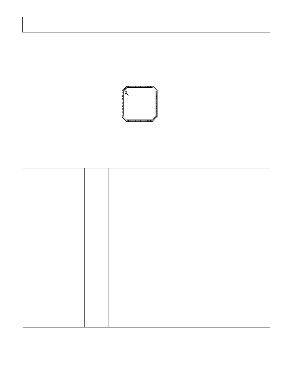
PIN CONFIGURATION AND FUNCTION DESCRIPTIONS
PIN 1
INDICATOR
NC = NO CONNECT
1
NC (Reserved)
2
SDATA_OUT
3
BIT_CLK
4
DV
SS
5
SDATA_IN
6
DV
DD
7
SYNC
8
RESET
24 PORT-D_R (Line Out)
23 PORT-D_L (Line Out)
22 AV
DD
(Optional)
21 SENSE_SRC
20 MIC_BIAS-C
19 MIC_BIAS-B
18 VREF_FILT
17 AV
SS
9
S
E
N
S
E
_
A
1
0
N
C
1
1
N
C
1
2
N
C
1
3
P
O
R
T
-
B
_
L
(
M
I
C
)
1
4
P
O
R
T
-
B
_
R
(
M
I
C
)
1
5
P
O
R
T
-
C
_
L
(
L
i
n
e
I
n
)
1
6
P
O
R
T
-
C
_
R
(
L
i
n
e
I
n
)
3
2
S
/
P
D
I
F
_
O
U
T
3
1
G
P
I
O
_
1
/
J
S
_
0
3
0
G
P
I
O
_
0
/
J
S
_
1
2
9
A
V
S
S
2
8
P
O
R
T
-
A
_
R
(
H
e
a
d
p
h
o
n
e
)
2
7
P
O
R
T
-
A
_
L
(
H
e
a
d
p
h
o
n
e
)
2
6
A
V
D
D
2
5
M
O
N
O
_
O
U
T
TOP VIEW
(Not to Scale)
AD1983
05
20
5-
0
02
Figure 2. Pin Configuration
Table 5. Pin Function Descriptions
Mnemonic
Pin
No. I/O
1
Description
SDATA_OUT
2
I
HD Audio Link Serial Data Output. Codec input stream.
BIT_CLK
3
I
HD Audio Link Bit Clock Input. 24 MHz.
SDATA_IN
5
I/O
HD Audio Link Serial Data Input. Codec output stream.
SYNC
7
I
HD Audio Link Frame Sync.
RESET
8
I
HD Audio Link Reset. Master hardware reset.
GPIO_1/JS_0
31
Digital I/O
GPIO_1: General Purpose Input/Output Pin. Digital signal used for circuit control.
JS_0: Classical (DC) Jack Sense for Line_Out Pins. Low = jack not present, high = jack
present.
GPIO_0/JS_1
30
Digital I/O
GPIO_0: General Purpose Input/Output Pin. Digital signal used circuit control.
JS_1: Classical (DC) Jack Sense for Headphone. Low = jack not present, high = jack
present.
SENSE_A 9
Digital
I
Jack Sense Input for Presence Detect on Port A Through Port D. Used with isolated
switches on audio jacks.
SENSE_SRC 21
Digital
O
Connect via 2.67 k 1% resistor to Pin 9 (SENSE_A) when using the SENSE_A functionality.
This reduces the current draw of the jack presence tree during idle states. Remove the
resistor between Pin 9 and AV
DD
in this mode.
PORT-B_L (MIC)
13
Analog I
Microphone or Line-In Left Input.
PORT-B_R (MIC)
14
Analog I
Microphone or Line-In Right Input.
PORT-C_L (Line In)
15
Analog I
Line-In or Microphone Left Input.
PORT-C_R (Line In)
16
Analog I
Line-In or Microphone Right Input.
PORT-D_L (Line Out)
23
Analog O
Line-Out-(Front)-Left Channel.
PORT-D_R (Line Out)
24
Analog O
Line-Out-(Front)-Right Channel.
MONO_OUT
25
Analog O
Monaural Output to Telephony Subsystem Speakerphone.
PORT-A_L (Headphone)
27
Analog O
Headphone-Out-Left Channel.
PORT-A_R (Headphone)
28
Analog O
Headphone-Out-Right Channel.
VREF_FILT
18
O
Voltage Reference Filter.
MIC_BIAS-B
19
O
Programmable Microphone Bias Output. Intended for connection to Port-B.

AD1983
Rev. 0 | Page 8 of 16
Mnemonic
Pin
No. I/O
1
Description
MIC_BIAS-C
20
O
Programmable Microphone Bias Output. Intended for connection to Port-C.
DV
SS
4
I
Digital Supply Return (Ground).
DV
DD
6
I
Digital Supply Voltage (3.3 V).
AV
SS
17, 29
I
Analog Supply Return (Ground).
AV
DD
22, 26
I
Analog Supply Voltage (5.0 V). AV
DD
supplies should be well filtered because supply noise
degrades audio performance. Connection to Pin 22 is optional.
S/PDIF_OUT
32
Digital O
Supports S/PDIF Output.
NC
1, 10
to 12
1
I refers to input and O refers to output.
AD1983
Rev. 0 | Page 9 of 16
HD AUDIO CODEC INFORMATION
Table 6. Widget List and Descriptions
NID
(Hex) Name
Type
ID Type
Description
00 ROOT
x
Root
Device
identification.
01
FUNCTION
x
Function
Designates this device as an audio codec.
02
S/PDIF
0
Audio output
Designates the codec S/PDIF digital stream output interface.
03
Front DAC
0
Audio output
Designates the playback channel digital/audio converters.
04
Record ADC
1
Audio input
Designates the record channel audio/digital converters.
05
Port-D (Line Out)
4
Pin complex
Port-D pin drivers. Typically used as rear panel line output.
06
Port-A (Headphone Out)
4
Pin complex
Port-A pin drivers. Typically used as front panel headphone output.
07 MONO_OUT
4
Pin
complex Monaural output pin driver. Typically used to drive an internal
speaker or as a microphone selector on a telephony system.
08
Port-B (Front Microphone)
4
Pin complex
Port-B pin drivers. Typically used as front panel microphone.
09
Port-C (Line In)
4
Pin complex
Port-C pin drivers. Typically used as rear panel line input.
0A
S/PDIF_OUT
4
Pin complex
S/PDIF output digital interface.
0B
Mono Selector
3
Audio selector
Chooses the signals that drive the mono output mixer and pin.
0C
Microphone Selector/Boost
3
Audio mixer
Allows microphone source port selection and boost preamplifier
setting.
0D
Line In Selector
3
Audio selector
Allows line in source port selection.
0E
Analog Mixer
2
Audio mixer
Selectively mixes analog input signals into a single signal.
0F
Mono Mixer
2
Audio mixer
Stereo-to-Mono mixer.
10
Digital PC Beep
7
Beep generator
Digital PC beep generator.
11
Front Mix Amp
3
Audio selector
Individual gain control for the DAC (front) input to the analog mixer.
12
Port-B Mix Amp
3
Audio selector
Individual gain control for the Port-B (front microphone) input to the
analog mixer.
13
Port-C Mix Amp
3
Audio selector
Individual gain control for the Port-C (line in) input to the analog
mixer.
14
Record Selector
3
Audio selector
Chooses the signal that is recorded by the record ADC. Also contains
the record gain controls.
15 Analog
Power-Down
5
Power
widget
Controls power on analog mixer and associated amplifiers. This
controls the power of all widgets in its connection list.
Table 7. Root and Function Node Parameters
1
Type
Vendor ID
Revision ID
Sub Node
Count
Function Group
Type
Audio
F.G. Caps
GPIO Caps
NID (Hex)
Name
ID
Type
PID 00
2
PID
02
2
PID
04
2
PID
05
2
PID
08
2
PID
11
2
00 ROOT
X
Root
11D41983
00100400
00010001
01 FUNCTION
X
Function
00020014
00000001 00010C0C
40000002
1
Default SSID: BFD30000.
2
PID = parameter ID.

AD1983
Rev. 0 | Page 10 of 16
Table 8. Widget Parameters
NID
Widget
Caps
PCM Size,
Rate
Stream
Format
Pin
Caps
Input
Amp Caps
Con. List
Len
Power
States
Processing
Caps
GPIO
Caps
Vendor-
Specific
(Hex) Name
PID 09
1
PID
0A
1
PID
0B
1
PID
0C
1
PID
0D
1
PID
0E
1
PID
0F
1
PID
10
1
PID
11
1
PID
F0
1
01 FUNCTION
000004C0
000E007F
00000001
00000000
00000009 00000001 80053F3D 00000084
02 S/PDIF
00030311
00020060
00000005
00000002
03 Front
DAC
00000441
000E007F
00000001
00000000 00000009 00004601
00000010
04 Record
ADC
00100501
000E007F
00000001
00000001 00000009
05
Port-D (Line Out) 00400185
00000017
00000002
80053F3D 00000008
06
Port-A
(Headphone Out)
00400185
0000001F
00000002
80053F3D 00000008
07 MONO_OUT 00400104
00000010
00000001
80053F3D
08
Port-B (Front
Microphone)
00400081
00001727
00000000
00000008
09
Port-C (Line In)
00400081
00001727
00000000
00000008
0A S/PDIF_OUT
00400301
00000010
00000001
0B Mono
Selector 00300101
00000004
0C
Microphone
Selector/Boost
0030010D
00000002
00270300
0D
Line In Selector
00300101
00000002
0E Analog
Mixer 00200101
00000003
0F Mono
Mixer
00200100
00000001
00000002
10
Digital PC Beep
0070000C
00000000
800B0F0F
11
Front Mix Amp
0030010D
00000001
80051F17
12
Port-B Mix Amp 0030010D
00000001
80051F17
13
Port-C Mix Amp 0030010D
00000001
80051F17
14 Record
Selector
0030010D
00000004
80050F00
15
Analog Power-
Down
00500500
00000004 00000009
1
PID = parameter ID.
AD1983
Rev. 0 | Page 11 of 16
Table 9. Default Configuration Parameters
Bit
31 29 27 23 19
15 8 7
3
Bit
30 28 24 20 16
12 8 4
0
Location
Misc.
Node
ID
(Hex) Name
Type
ID Value Connect
Chassis
Position
Def.
Device
Conn.
Type Color Ovrrd.
Def.
Assn. Sequence
05 Line
Out 4 01014010
Jack External
Rear Line
Out
1/8"
Jack
Green 0 1 0
06
HP Out
4
0221401F
Jack
External
Front
HP Out
1/8"
Jack
Green 0 1 F
07
Mono Out
4
991301F0
Fixed
Internal
Special 3
Speaker
ATAPI
Unknown
1
F
0
08
Microphone
In
4 02A19020
Jack External
Front Mic
In
1/8"
Jack
Pink 0 2 0
09
Line In
4
0181302E
Jack
External
Rear
Line In
1/8"
Jack
Blue 0 2 E
0A S/PDIF
Out
4 014511F0
Jack External
Rear SPDIF
Out
Optical Black
1
F
0
Table 10. Widget Connection List
Index
0
1
2
3
NID (Hex)
Name
NID (Hex)
NID (Hex)
NID (Hex)
NID (Hex)
02
S/PDIF
01
04
03
Front DAC
04
Record ADC
14
05
Port-D (Line Out)
03
0E
06
Port-A (Headphone Out)
03
0E
07 MONO_OUT
0F
08
Port-B (Front Microphone)
09
Port-C (Line In)
0A S/PDIF_OUT
02
0B Mono
Selector
03
0C 0D 0E
0C
Microphone Selector/Boost
08
09
0D
Line In Selector
09
08
0E
Analog Mixer
11
12
13
0F
Mono Mixer
0B
10
Digital PC Beep
11
Front Mix Amp
03
12
Port-B Mix Amp
0C
13
Port-C Mix Amp
0D
14 Record
Selector
0C
0D 0E 0F
15 Analog
Power-Down
05
09 0B 14
AD1983
Rev. 0 | Page 12 of 16
VERB SUPPORT
Table 11 and Table 12 list only those HD audio verbs that are supported.
Table 11. Widget Verb Support
Stream
Format
A
m
plif
i
e
r
Gai
n/Mute
Processi
ng
Coef
fic
i
ent
Coff
ici
e
nt
Index
P
a
ram
e
te
r
Connectio
n
Select
Connectio
n
List Entry
Processi
ng
State
SDI Select
Power State
Chann
e
l /
Stream ID
Pin W
i
dg
et
Control
Unsoli
ci
ted
Enable
Pin Se
nse
Beep
Ge
ne
ra
tor
Di
gi
tal
Conv
erter 1
Di
gi
tal
Conv
erter 2
Get
(Hex)
Axx Bxx Cxx Dxx F00 F01 F02 F03 F04 F05 F06 F07 F08 F09 F0A
F0D
Node
ID
(Hex)
Name
Set
(Hex)
2xx 3xx 4xx 5xx --- 701 --- 703 704 705 706 707 708 709 70A 70D 70E
00
ROOT
01 FUNCTION
S
1
S
1
U
2
02 S/PDIF
S
1
U
2
03 Front
DAC
U
2
04 Record
ADC
U
2
05 Line
Out
06 HP
Out
07
Mono Out
08
Microphone In
09
Line In
0A
S/PDIF Out
0B
Mono Selector
0C
Microphone
Selector
0D
Line In Selector
0E
Analog Mixer
0F
Mono Mixer
10
Digital PCBeep
11
Front MixAmp
12
Microphone
MixAmp
13
Line In MixAmp
14
ADC Selector
15
Analog Power
Down
1
S = supports ADI specific functionality. Refer to the Programming Guide for more details (available from your assigned Applications Engineer).
2
U = unsupported in the AD1983; the get verb always returns 0, the set verbs are ignored.
AD1983
Rev. 0 | Page 13 of 16
Table 12. Widget Extended Verb Support
GPI/O Da
ta
GPI/O
Enable
GPI/O
Dir
e
c
t
ion
GPI/O W
a
k
e
Mas
k
GPI/O
Unsolicited
GPI/O
Sticky Mas
k
Co
n
f
i
g
D
e
f
Byte1
Co
n
f
i
g
D
e
f
Byte2
Co
n
f
i
g
D
e
f
B
y
te
3
Co
n
f
i
g
D
e
f
B
y
te
4
Subsy
st
e
m
ID B
y
te
1
Subsy
st
e
m
ID B
y
te
2
Subsy
st
e
m
ID B
y
te
3
Subsy
st
e
m
ID B
y
t
e
4
Get
(Hex) F15 F16 F17 F18 F19 F1A
F1C
F20
Node ID
Name
Set
(Hex) 715 716 717 718 719 71A 71C 71D 71E 71F 720 721 722 723
01
1
FUNCTION
U
2
U
2
05
Line
Out
06
HP
Out
07
Mono
Out
08
Microphone
09
Line
In
0A S/PDIF
Out
1
Only the FUNCTION node (Node ID 01) supports the RESET Verb 7FF (set verb only).
2
U = unsupported in the AD1983. The get verb always returns 0, and the set verbs are ignored.
AD1983
Rev. 0 | Page 14 of 16
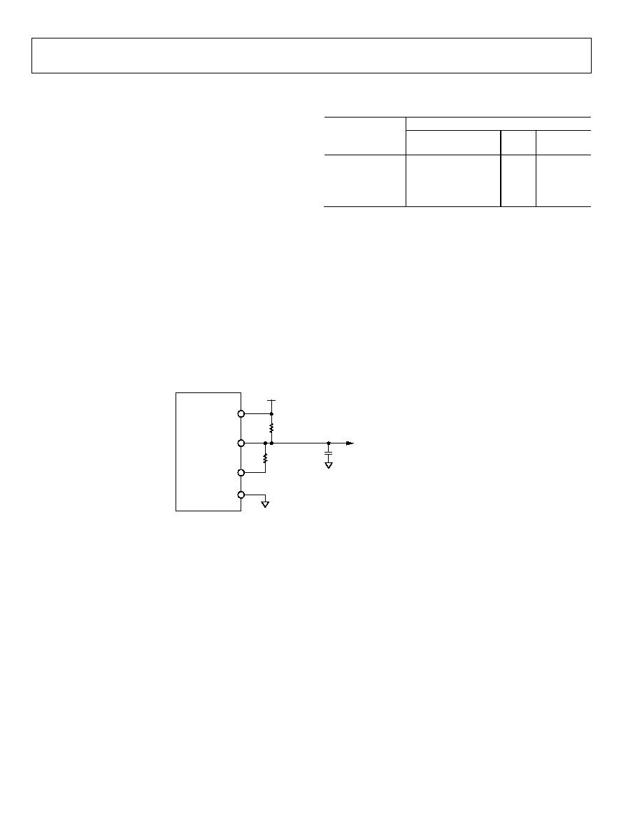
JACK PRESENCE DETECTION
The AD1983 uses one jack sense line for presence detection on
up to four external jacks. This enables software to determine if
there is a device plugged into a jack; then, the AD1983 sensing
engine can determine what type of device it is. Jack presence is
detected using a resistor tree arrangement outlined in the HD
Audio specification. Up to four jacks can be sensed on a single
sense line by using a different value resistor for each between
the sense line and ground (AV
SS
). Jacks must have normally-
open, isolated switches to use this method of jack presence
detection.
For proper operation there must be a 2.67 k 1% resistor
connected between SENSE_A and AV
DD
. For this configuration
R1 and C1 should be installed; R2 should not be installed
(see Figure 3).
The specific resistor values for each jack are shown in Table 13.
To ensure accurate detection, use 1% tolerance resistors for all
jack presence circuitry.
Table 13. Jack Sense Mapping
SENSE_A
Resistor (1%)
Name
Port
Node ID
(Hex)
5.1 k
Line Out
D
05
10.0 k
Line In
C
09
20.0 k
Microphone
B
08
39.2 k
Headphone Out
A
06
An alternate method reduces the current for sensing by
connecting a single 2.67 k 1% resistor between the SENSE_A
and SENSE_SRC pins. For this configuration R1 and C1 are not
installed; however, R2 is installed (see Figure 3).
It is recommended that designers place circuitry for both
sensing methods and only install one of the two options.
SENSE_A/SRC_B
TO JACKS FOR
PORT A THROUGH PORT D
AD1983
C1
1µF
SENSE_SRC
AV
SS
22, 26
21
17, 29
9
AV
DD
AV
DD
R1
2.67k, 1%, 1/8W
R2 (DNE)
2.67k, 1%, 1/8W
05
20
5-
0
03
Figure 3. Jack Presence Detection
AD1983
Rev. 0 | Page 15 of 16
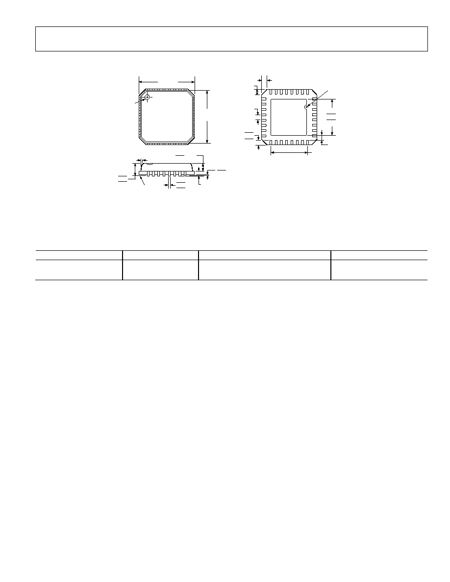
OUTLINE DIMENSIONS
COMPLIANT TO JEDEC STANDARDS MO-220-VHHD-2
0.30
0.23
0.18
0.20 REF
0.80 MAX
0.65 TYP
0.05 MAX
0.02 NOM
12∞ MAX
1.00
0.85
0.80
SEATING
PLANE
COPLANARITY
0.08
1
32
8
9
25
24
16
17
0.50
0.40
0.30
3.50 REF
0.50
BSC
PIN 1
INDICATOR
TOP
VIEW
5.00
BSC SQ
4.75
BSC SQ
3.65
3.50 SQ
3.35
PIN 1
INDICATOR
0.60 MAX
0.60 MAX
0.25 MIN
EXPOSED
PAD
(BOTTOM VIEW)
Figure 4. 32-Lead Lead Frame Chip Scale Package [LFCSP_VQ]
5 mm ◊ 5 mm Body, Very Thin Quad
(CP-32-4)
Dimensions shown in millimeters
ORDERING GUIDE
Model
Temperature Range
Package Description
Package Option
AD1983JCPZ
1
0
∞C to +70∞C
32-Lead LFCSP_VQ, Tray
CP-32-4
AD1983JCPZ-REEL
1
0
∞C to +70∞C
32-Lead LFCSP_VQ, Reel
CP-32-4
1
Z = Pb-free part.

AD1983
Rev. 0 | Page 16 of 16
NOTES
©2006 Analog Devices, Inc. All rights reserved. Trademarks and
registered trademarks are the property of their respective owners.
D05205-0-4/06(0)