Äîêóìåíòàöèÿ è îïèñàíèÿ www.docs.chipfind.ru
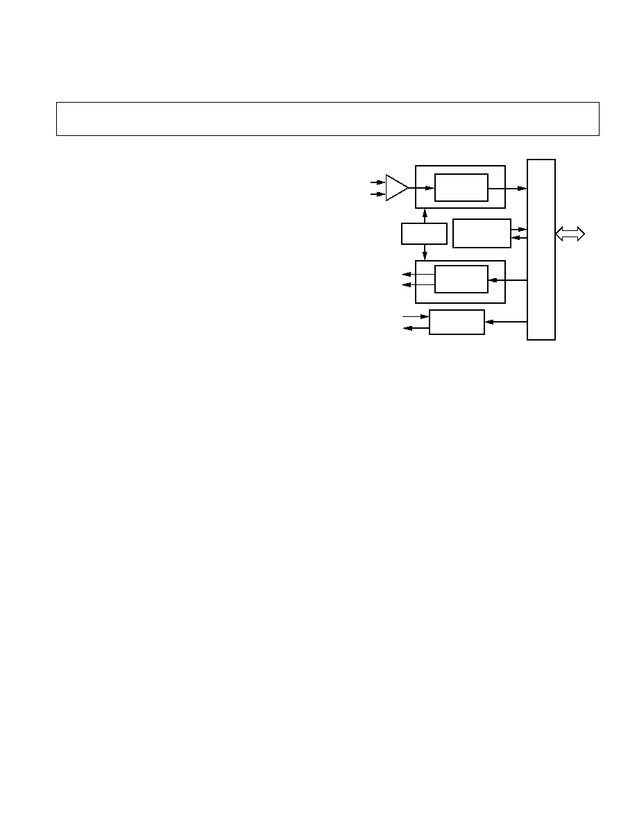
FUNCTIONAL BLOCK DIAGRAM
16-BIT
SIGMA-DELTA
DAC
ANALOG
INPUTS
RESAMPLING
INTERPOLATION
FILTER
DIFFERENTIAL
ANALOG
OUTPUT
CLOCK INPUTS
CLOCK OUTPUTS
CLOCK
GENERATION
SERIAL
PORT
DIGITAL
DATA AND
CONTROL
VOLTAGE
REFERENCE
16-BIT
SIGMA-DELTA
ADC
REV. A
Information furnished by Analog Devices is believed to be accurate and
reliable. However, no responsibility is assumed by Analog Devices for its
use, nor for any infringements of patents or other rights of third parties
which may result from its use. No license is granted by implication or
otherwise under any patent or patent rights of Analog Devices.
a
PSTN Signal Port
AD28msp01
One Technology Way, P.O. Box 9106, Norwood, MA 02062-9106, U.S.A.
Tel: 617/329-4700
Fax: 617/326-8703
FEATURES
Complete Analog l/O Port for DSP-Based FAX/MODEM
Applications
Linear-Coded 16-Bit Sigma-Delta ADC
Linear-Coded 16-Bit Sigma-Delta DAC
On-Chip Anti-Alias and Anti-lmage Filters
Digital Resampling/lnterpolation Filter
7.2 kHz, 8.0 kHz, and 9.6 kHz Sampling Rates
8/7 Mode for 8.23 kHz, 9.14 kHz, and 10.97 kHz
Sampling Rates
Synchronous and Asynchronous DAC/ADC Modes
Bit and Baud Clock Generation
Transmit Digital Phase-Locked Loop for Terminal
Synchronization
Independent Transmit and Receive Phase Adjustment
Serial Interface to DSP Processors
+5 V Operation with Power-Down Mode
28-Pin Plastic DlP/44-Lead PLCC/28-Lead SOIC
APPLICATIONS
High Performance DSP-Based Modems
V.32ter, V.32bis, V.32, V.22bis, V.22, V.21,
Bell 212A, 103
Fax and Cellular-Compatible Modems
V.33, V.29, V.27ter, V.27bis, V.27, V.26bis
Integrated Fax, Modem, and Speech Processing
GENERAL DESCRIPTION
The AD28msp01 is a complete analog front end for high perfor-
mance DSP-based modems. The device includes all data conver-
sion, filtering, and clock generation circuitry needed to imple-
ment an echo-cancelling modem with a single host digital signal
processor. Software-programmable sample rates and clocking
modes support all established modem standards. The AD28msp01
simplifies overall system design by requiring only +5 volts.
The inclusion of on-chip anti-aliasing and anti-imaging filters
and 16-bit sigma-delta ADC and DAC ensures a highly inte-
grated and compact solution for FAX or data MODEM applica-
tions. Sigma-delta conversion technology eliminates the need for
complex off-chip anti-aliasing filters and sample-and-hold circuitry.
The AD28msp01 utilizes advanced sigma-delta technology to
move the entire echo-cancelling modem implementation into the
digital domain. The device maintains a 72 dB SNR throughout
all filtering and data conversion. Purely DSP-based echo cancel-
lation algorithms can thereby maintain robust bit error rates
under worst-case signal attenuation and echo amplitude condi-
tions. The AD28msp01's on-chip interpolation filter resamples
the received signal after echo cancellation in the DSP, freeing
the processor for other voice or data communications tasks.
On-chip bit and baud clock generation circuitry provides for
either synchronous or asynchronous operation of the transmit
(DAC) and receive (ADC) paths. Each path features indepen-
dent phase advance and retard adjustments via software control.
The AD28msp01 can also synchronize modem operation to an
external terminal bit clock.
The AD28msp01's serial I/O port provides an easy interface to
host DSP microprocessors such as the ADSP-2101, ADSP-2105,
and ADSP-2111. Packaged in a 28-pin plastic DIP, 44-lead
PLCC, 44-pin TQFP, or 28-lead SOIC, the AD28msp01 pro-
vides a compact solution for space-constrained environments.
The device operates from a +5 V supply and offers a low power
sleep mode for battery-powered systems.
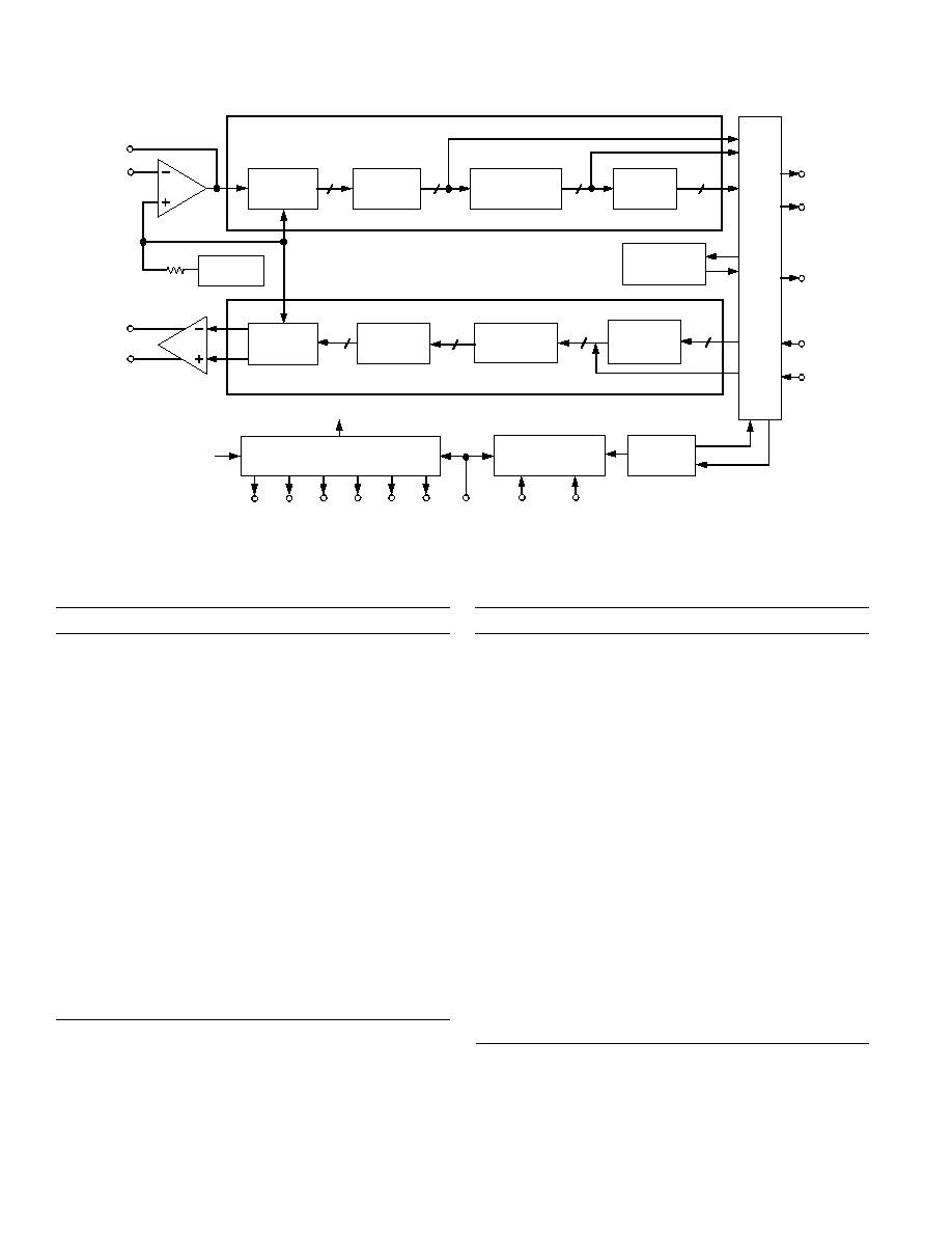
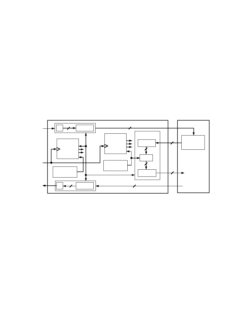
A detailed block diagram of the AD28msp01 is shown in
Figure 1.
AD28msp01
REV. A
2
CS
t
CONV
t
BAUD
t
BIT
M
CLK
RESET
ANALOG
SIGMA-DELTA
MODULATOR
DIGITAL
DECIMATION
FILTER
DIGITAL
ANTI-ALIASING
LOW-PASS FILTER
DIGITAL
HIGH-PASS
FILTER
RESAMPLING
INTERPOLATION
FILTER
SERIAL
PORT
1
1.728 MHz
16
28.8/32.0/38.4 kHz
16
7.2/8.0/9.6 kHz
16
7.2/8.0/9.6 kHz
SDI
SDIFS
SDO
SDOFS
SCLK
V
IN
VOLTAGE
REFERENCE
ANALOG
SMOOTHING
FILTER
DIGITAL
SIGMA-DELTA
MODULATOR
DIGITAL
INTERPOLATION
FILTER
DIGITAL
ANTI-IMAGING
LOW-PASS
FILTER
1
1.728 MHz
16
1.728 MHz
16
28.8/32.0/38.4 kHz
16
7.2/8.0/9.6 kHz
V
OUT+
V
OUT
V
FB
OUTPUT
DIFF.
AMP
TSYNC
r
CONV
r
BAUD
r
BIT
CLOCK GENERATION
CONTROL
REGISTERS
INTERNAL CLOCK
CONTROL CIRCUITRY
AND
SEQUENCER
500k
16-BIT SIGMA-DELTA ADC
16-BIT SIGMA-DELTA DAC
INPUT
AMP
Figure 1. AD28msp01 Block Diagram
PIN DESCRIPTIONS
Name
Type Description
Analog Interface
V
IN
I
Analog input to the inverting terminal of the
input amplifier.
V
FB
O
Feedback terminal of the input amplifier.
V
OUTP
O
Analog output from the noninverting terminal
of the output differential amplifier.
V
OUTN
O
Analog output from inverting terminal of the
output differential amplifier.
Serial Interface
SCLK
O/Z
Serial clock used for clocking data or control
bits to/from the serial port (SPORT). The
frequency of this clock is 1.7280 MHz. This
pin is 3-stated when the CS is low.
SDI
I
Serial data input of the SPORT. Both data
and control information are input on this pin.
This pin is ignored when CS is low.
SDO
O/Z
Serial data output of the SPORT. Both data
and control information are output on this
pin. This pin is 3-stated when CS is low.
SDIFS
I
Framing synchronization signal for serial data
transfers to the AD28msp01 (via the SDI
pin). This pin is ignored when CS is low.
Name
Type Description
SDOFS
O/Z
Framing synchronization signal for serial data
transfers from the AD28msp01 (via the SDO
pin). This pin is 3-stated when CS is low.
Clock Generation
TSYNC
I
Transmit synchronization clock. This signal is
used to synchronize the transmit clocks and
the converter clocks to an external terminal/
bit-rate clock. It is used in the V.32 TSYNC
and Asynchronous TSYNC modes and is
ignored in other operating modes. The
frequency of the external clock must be
programmed in Control Register 0. This pin
must be tied high or low if it is not being
used.
TBIT
O
Transmit bit rate clock. This is an output
clock whose frequency is programmable via
Control Register 3. It is synchronized with
the TCONV clock.
TBAUD O
Transmit baud rate clock. This is an output
clock whose frequency is programmable via
Control Register 3. It is synchronized with
the TCONV clock.

AD28msp01
REV. A
3
PIN DESCRIPTIONS (Continued)
Name
Type Description
TCONV O
Transmit conversion clock. This clock indicates
when the ADC has finished a sampling cycle.
The frequency of TCONV is programmed by
setting the sample rate field in Control Register
0. The programmed TCONV rate can be scaled
by a factor of 8/7 by setting Bit 9 in Control
Register 1. The phase of TCONV can be
adjusted by writing the Transmit Phase Adjust
Register (Control Register 5).
RBIT
O
Receive bit rate clock. This is an output clock
whose frequency is programmable via Control
Register 2. It is synchronized with the RCONV
clock.
RBAUD O
Receive baud rate clock. This is an output clock
whose frequency is programmable via Control
Register 2. It is synchronized with the RCONV
clock.
RCONV O
Receive conversion clock. This clock indicates
when the DAC has finished a sampling cycle.
The frequency of RCONV is programmed by
setting the sample rate field in Control Register
0. The programmed RCONV rate can be scaled
by a factor of 8/7 by setting Bit 9 in Control
Register 1. The phase of RCONV can be
adjusted by writing the Receive Phase Adjust
Register (Control Register 4).
Miscellaneous
MCLK
I
AD28msp01 master clock input. The frequency
of this clock must be 13.824 MHz to guarantee
listed specifications.
RESET
I
Active-low chip reset. This signal sets all
AD28msp01 control registers to their default
values and clears the device's digital filters.
SPORT output pins are 3-stated when RESET
is low. SPORT input pins are ignored when
RESET
is low.
CS
I
Active-high chip select. This signal 3-states all
SPORT output pins and forces the AD28msp01
to ignore all SPORT input pins. If CS is
deasserted during a serial data transfer, the
16-bit word being transmitted is lost.
Power Supplies
V
CC
Analog supply voltage (nominally +5 V)
GND
A
Analog ground
V
DD
Digital supply voltage (nominally +5 V)
GND
D
Digital ground
FUNCTIONAL DESCRIPTION
A/D Conversion
The A/D conversion circuitry of the AD28msp01 consists of an
analog input amplifier and a sigma-delta analog-to-digital con-
verter (ADC). The analog input signal to the AD28msp01 must
be ac coupled.
Analog Input Amplifier
The analog input amplifier is internally biased by an on-chip
voltage reference in order to allow operation of the AD28msp01
with a +5 V power supply.
Input signal level to the sigma-delta modulator should not ex-
ceed V
INMAX
, which is specified under "Analog Interface Electri-
cal Characteristics." Refer to "Analog Input" in the "Design
Considerations" section of this data sheet for more information.
ADC
The ADC consists of a 3rd-order analog sigma-delta modulator,
a decimation filter, an anti-aliasing low-pass filter, and a high-
pass filter. The analog input is applied to the input amplifier.
The output of this amplifier is applied to an analog sigma-delta
modulator which noise-shapes it and produces 1-bit samples at
a 1.7280 MHz rate. This bit stream is fed to the decimation
filter, which increases the resolution to 16-bits and decreases the
sampling frequency. The parallel data stream is then processed
by the anti-aliasing low-pass filter which further reduces the
sampling rate. Finally, the high-pass filter removes input fre-
quency components at the low end of the spectrum.
Either the high-pass filter alone or the high-pass/anti-aliasing
low-pass filter combination can be bypassed by setting the
appropriate bits in Control Register 1, thus producing samples
at 7.2/8.0/9.6 kHz or 28.8/32.0/38.4 kHz, respectively. The gain
and the frequency response of the AD28msp01 are altered when
these filters are bypassed. The DSP processor that receives
samples from the AD28msp01 may need to compensate for this
change.
Decimation Filter
The decimation filter is a sinc
4
digital filter that increases resolu-
tion to 16 bits and reduces the sample rate to 28.8, 32.0, or
38.4 kHz (depending on the input sample rate). The 16 bit, par-
allel data stream output of the decimation filter is then pro-
cessed by the anti-aliasing low-pass filter.
Anti-Aliasing Low-Pass Filter
The anti-aliasing low-pass filter further reduces the sampling
rate by a factor of four to 7.2 kHz, 8.0 kHz, or 9.6 kHz (de-
pending on the output sample rate of the decimation filter). The
output is fed to the high-pass filter. The low-pass/high-pass filter
combination can be bypassed by setting the appropriate bits in
Control Register 1. If the filters are bypassed, the signal must be
scaled by the following multipliers to achieve normal levels:
2.046 for 9.6 kHz, 0.987 for 8.0 kHz, and 0.647 for 7.2 kHz.
When the filters are bypassed, the host DSP must be able to re-
ceive data at the 28.8/32.0/38.4 kHz rates. In this case,
resampling interpolation should be disabled because of insuffi-
cient bandwidth to transmit both ADC and resampled data to
the SPORT.
High-Pass Filter
The digital high-pass filter removes frequency components at
the low end of the spectrum. The high pass filter can be by-
passed by setting the appropriate bits in Control Register 1.
AD28msp01
REV. A
4
The output of the ADC is transferred to the AD28msp01's se-
rial port (SPORT) for transmission to the host DSP processor.
D/A CONVERSION
The D/A conversion circuitry of the AD28msp01 consists of a
sigma-delta digital-to-analog converter (DAC) and a differential
output amplifier.
DAC
The DAC consists of an anti-imaging low-pass filter, an interpo-
lation filter, a digital sigma-delta modulator, and an analog
smoothing filter. These filters have the same characteristics as
the ADC's anti-aliasing filter and decimation filter.
The DAC receives 16-bit samples from the host DSP processor
via AD28msp01's SPORT. If the host processor fails to write a
new value to the serial port, the existing (previous) data is read
again. The data stream is filtered first by the DAC's anti-
imaging low-pass filter and then by the interpolation filter. The
output of the interpolation filter is fed to the DAC's digital
sigma-delta modulator, which converts the 16-bit data to 1-bit
samples. The output of the sigma-delta modulator is fed to the
AD28msp01's analog smoothing filter where it is converted into
a low-pass filtered, analog voltage.
Anti-lmaging Low-Pass Filter
The anti-imaging low-pass filter filters the 7.2 kHz, 8.0 kHz, or
9.6 kHz data stream form the SPORTs, and raises the sampling
rate to 28.8 kHz, 32.0 kHz, or 38.4 kHz.
The anti-imaging low-pass filter can be bypassed by setting the
appropriate bit in Control Register 1. This results in a gain
change. If the filter is bypassed, the signal must be scaled by the
following multipliers to achieve normal levels: 2.046 for 9.6 kHz,
0.987 for 8.0 kHz, and 0.647 for 7.2 kHz.
When the filter is bypassed, the host DSP must be able to trans-
mit data at the 28.8/32.0/38.4 kHz rates. In this case, re-
sampling interpolation should be disabled because of
insufficient bandwidth to transmit both ADC and resampled
data to the SPORT.
Interpolation Filter
The interpolation filter contains is a sinc
4
digital filter which
raises the sampling rate to 1.7280 MHz by interpolating be-
tween the samples. These 16-bit samples are then processed by
the digital sigma-delta modulator which noise-shapes the data
stream and reduces the sample width to a single bit stream.
Analog Smoothing Filter
The AD28msp01's analog smoothing filter consists of a 2nd-
order Sallen-Key continuous-time filter and a 3rd-order switched
capacitor filter. The Sallen-Key filter has a 3 dB point at
approximately 80 kHz.
The analog smoothing filter converts the 1.7280 MHz bit
stream output of the sigma-delta modulator into a low-pass
filtered, differential analog signal.
Differential Output Amplifier
The differential output amplifier produces the AD28msp01's
analog output (V
OUTP
, V
OUTN
). It can drive loads of 2 k
or
greater and has a maximum differential output voltage swing of
6.312 V peak-to-peak. The output signal is dc biased to the
AD28msp01's on-chip voltage reference (2.5 V nominal) and
can be ac coupled directly to a load or dc coupled to an external
amplifier. Refer to "Analog Output" in the "Design Consider-
ations" section of this data sheet for more information.
The V
OUTP
and V
OUTN
outputs must be used as differential out-
puts; do not use either as a single-ended output.
SERIAL PORT
The AD28msp01 includes a full-duplex synchronous serial port
(SPORT) used to communicate with a host processor. The
SPORT is used to read and write all data and control registers
in the AD28msp01. The SPORT transfers 16-bit words, MSB
first, at a serial clock rate of 1.7280 MHz.
When the AD28msp01 exits reset, both the analog circuitry and
the digital circuitry are powered down. The serial port will not
transmit data to the host until the host sets the digital power-
down bit (PWDD) to 1 in Control Register 1. All control regis-
ters should be initialized before this bit is set.
The SPORT is configured for an externally generated receive
frame sync (SDIFS), an internally generated serial clock
(SCLK), and an internally generated transmit frame sync
(SDOFS). The host processor should be configured for an ex-
ternal serial clock and receive frame sync and an internal trans-
mit frame sync.
DSP Processor Interface
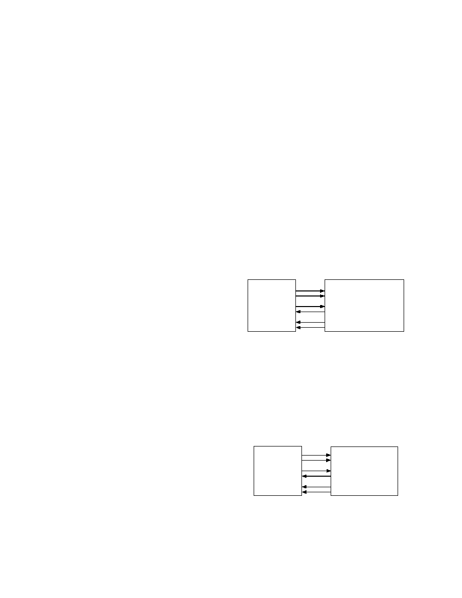
The AD28msp01-to-host processor interface is shown in
Figure 2.
SDO
SDOFS
SCLK
CS
SDI
SDIFS
SERIAL DATA RECEIVE
RECEIVE FRAME SYNC
SERIAL CLOCK
FLAG
SERIAL DATA TRANSMIT
TRANSMIT FRAME SYNC
DSP PROCESSOR
AD28msp01
Figure 2. AD28msp01-to-DSP Processor Interface
The AD28msp01's chip select (CS) must be held high to enable
SPORT operation. CS can be used to 3-state the SPORT pins
and disable communication with the host processor.
To use the ADSP-2101 or ADSP-2111 as host DSP processor
for the AD28msp01, refer to Figure 3.
Note that the ADSP-2101's SPORT0 communicates with the
AD28msp01's SPORT while the ADSP-2101's Flag Output
(FO) is used to signal the AD28msp01's CS input. SPORT1 on
the ADSP-2101 must be configured for flags and interrupts in
this system.
SDO
SDOFS
SCLK
CS
SDI
SDIFS
DR0
RFS0
SCLK0
FO
DT0
TFS0
ADSP-2101
AD28msp01
Figure 3. AD28msp01-to-ADSP-2101 Interface
Figure 4 shows an ADSP-2101 assembly language program that
initializes the AD28msp01 and implements a digital loopback
through the processor.

AD28msp01
REV. A
5
{This ADSP-2101 program initializes the AD28msp01}
{and executes a loopback, or talk-through, routine.}
. MODULE/RAM/BOOT = 0 MSP01;
. VAR/DM/CIRC rec[2];
{Receive word buffer}
. VAR/DM/CIRC trans[2];
{Transmit word buffer}
{lnterrupt Vectors}
rset:
JUMP start;
RTI; RTI; RTI;
irq2v:
RTI; RTI; RTI; RTI;
sprt0t:
AX0 = 0x25; DM(0x3ff3) = AX0;
{Disable TX autobuffer}
RTI; RTI;
sprt0r:
JUMP receive;
RTI; RTI; RTI;
sprt1t:
RTI; RTI; RTI; RTI;
sprt1r:
RTI; RTI; RTI; RTI;
timerv:
RTI; RTI; RTI; RTI;
{Initialize DAGs}
start:
I2 = ^ re c ;
L2 = %rec;
I3 = ^ trans;
L3 = %trans;
M0 = 0;
M1 = 1;
S1 = 0;
DM(0x3000) = SI;
{Reset the AD28msp01}
{Initialize the ADSP-2101}
init dsp:
AX0 = 0x2a0f;
{Ext RFS, Int TfS, Ext SCLK, SLEN = 15}
DM(0x3ff6) = AX0;
{SPORT0 control register}
AX0 = 0x101f;
{Enable SPORT0}
DM(0x3fff) = AX0;
{System control register}
{Initialize AD28msp01 control register}
init msp01:
{Note: This section could be autobuffered.}
IMASK = 0x10;
{Enable SPORT0 TX interrupt}
AR = 0;
CNTR = 6;
DO initi UNTIL CE;
TX0 = AR;
{Transmit address}
IDLE;
TX0 = SI;
{Transmit control word}
IDLE;
AY0 = AR;
initi:
AR = AY0 +1;
{Increment address}
AX1 = 1;
AR = 0x18;
{Power up AD28msp01}
TX0 = AX1;
IDLE;
TX0 = AR;
AR = B#0025;
{Enable RX autobuffering with I2, M1}
DM(0x3ff3) = AR;
{Autobuffer control register}
IMASK = 0x18;
{Enable RX and TX interrupt}
wait:
JUMP wait;
{Wait for receive interrupt}
{Receive Interrupt Routine}
receive:
DM(0x3ff3) = SI;
{Disable autobuffering}
AX1= DM(I2, M1);
{Read first receive word from buffer}

AD28msp01
REV. A
6
and receive timing as well as an additional clock signal for serial
port timing.
The receive clocks are the RCONV, RBIT and RBAUD signals.
The individual clock rates are programmable and are all syn-
chronized with RCONV.
The transmit clocks are the TCONV, TBIT and TBAUD sig-
nals. The individual clock rates are programmable and are all
synchronized with TCONV.
Depending on the operating mode, the converter clocks can be
synchronized to an external clock signal (TSYNC) or can be
generated internally. The clocks can be adjusted in phase by set-
ting the appropriate phase adjust register. All the AD28msp01
Bit/Baud clocks have a 50% duty cycle except the 1600 Hz baud
rate. This baud rate has a 33%66% duty cycle.
Resampling Interpolation Filter
The resampling interpolation filter interpolates the data from
the TCONV rate to 1.7280 MHz. The data is then resampled
(decimated) in phase with the RCONV clock. The frequency re-
sponse characteristics of the resampling interpolation filter are
identical to the frequency response characteristics of the anti-
imaging, low-pass filter/interpolation filter combination.
Figure 5 illustrates the effects of a resampling interpolation
filter.
ANALOG SIGNAL
SAMPLED AT 9600 Hz
OUTPUT OF
INTERPOLATION
FILTER
OUTPUT OF
RESAMPLING
FILTER
Figure 5. Effects of Interpolation Filter
AX0 = DM(I2, M1);
{Read data word}
AY0 = 8;
{Verify AD28msp01 address = 8}
AR = AX1 AY0;
IF EQ JUMP goodstuff;
RTI;
goodstuff;
MODIFY (I3, M1);
{Point to second word of TX buffer}
DM(I3, M0) = AX0;
MX1 = 6;
{Load address word into MX1}
AR = 0x06a7;
{Enable TX and RX autobuffer}
DM(0x3ff3) = AR;
{Write to SPORT control Register}
TX0 = MX1;
{Autobuffer start}
RTI;
.ENDMOD;
Figure 4. AD28msp01 Initialization and ADSP-2101 Loopback Routine
Serial Data Output
When the digital power-down bit (PWDD) of Control Register 1
is set to 1, the AD28msp01's SPORT begins transmitting data to
the host processor. All transfers between the host processor and
the AD28msp01 consist of a serial data output frame sync
(SDOFS) followed by a 16-bit address word, then a second
frame sync followed by a 16-bit data word. Address/data word
pairs are transmitted whenever they become available. The
ADC takes precedence over the Interpolator output data. If a
new word becomes available while a serial transfer is in progress,
the current serial transfer is completed before the new word starts
transmission.
Serial Data Input
The host processor must initiate data transfers to the
AD28msp01 by asserting the serial data input frame sync
(SDIFS) high. Each of the 16-bit address word and 16-bit data
word transfers begins one serial clock cycle after SDIFS is as-
serted. The address word always precedes the data word. The
second serial data input frame sync for the data word can be as-
serted as early as the last bit of the address word is transmitted,
or any time after.
The host processor must assert SDIFS shortly after the rising
edge of SCLK and must maintain SDIFS high for one cycle be-
cause SDIFS is clocked by the SCLK falling edge. Data is then
driven from the host processor shortly after the rising edge of
the next SCLK and is clocked into the AD28msp01 on the fall-
ing edge of SCLK in that cycle. Each bit of a 16-bit address and
16-bit data word is thus clocked into the AD28msp01 on the
falling edge of SCLK (MSB first).
If SDIFS is asserted high again before the end of the present
data word transfer, it is not recognized until the falling edge of
SCLK in the last (LSB) cycle.
When the serial port receives an interpolator or DAC input
word, it writes the value to an internal register which is read by
the AD28msp01 when it is needed. This allows the host to send
data words at any time during the sample period.
NOTE: Exact SPORT timing requirements are defined in the
"Specifications" section of this data sheet.
Clock Generation
The AD28msp01 generates all transmit and receive clocks
necessary to implement standard voice-grade modems. The
AD28msp01 can generate six different clock signals for transmit
AD28msp01
REV. A
7
Since the resample phase is locked to RCONV, it can be ad-
vanced or slipped by writing a signed-magnitude value to the
Receive Phase Adjust Register (Control Register 2). The phase
advance or slip is equal to the master clock period (13.824 MHz)
multiplied by the signed-magnitude 9-bit value in Control
Register 4.
The change in phase requires a maximum of two RCONV
cycles to complete. If the value written to Control Register 4 is
less than the oversampling ratio, then the change will complete
in one RCONV cycle.
Control Registers
The AD28msp01's six control registers configure the device for
various operating modes including filter bypass and power-
down. The AD28msp01's host processor can read and write to
the control register through the AD28msp01's serial port
(SPORT).
The control registers should be set up for the desired mode of
operation before bringing the AD28msp01 out of power-down
(by writing ones to the PWDA and PWDD bits in Control
Register 1).
The control registers are cleared (set to 0x0000) when the
AD28msp01 is reset.
The sampling rate should be set before writing ones to the
power-down bits. Changing the sampling rate at any other time
will force a soft reset. For more information about soft resets,
refer to the end of this section of the data sheet.
NOTE: Reserved bits should always be cleared to 0.
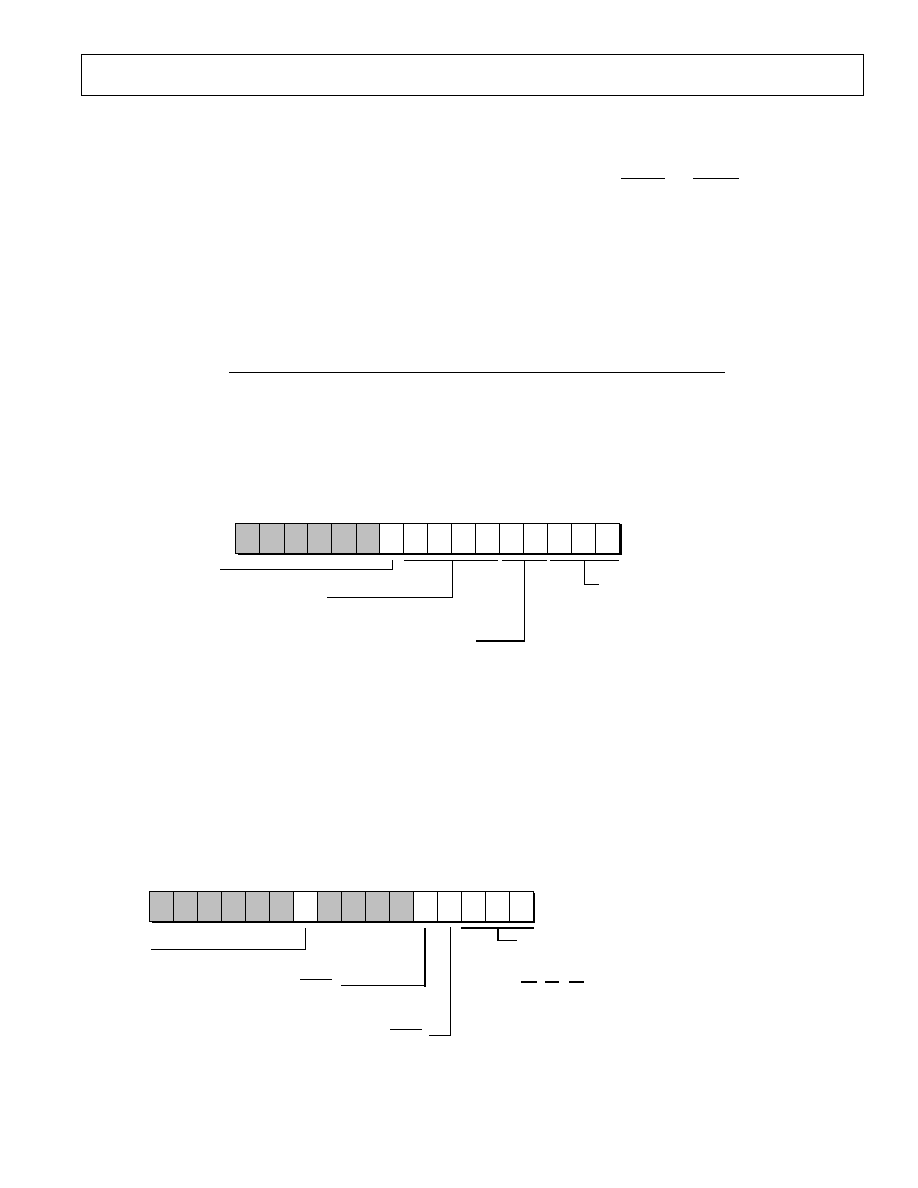
Control Register 0
address = 0x00
This register is used to:
· Enable/disable the resampling interpolation filter
· Set the external TSYNC clock rate
· Select the sampling rate
· Select the operating mode
15
14
13
12
11
10
9
8
7
6
5
4
3
2
1
0
0
0
0
0
0
0
0
0
0
0
0
0
0
0
0
0
TS3-0
TSYNC Rate (Hz)
0000 = 9600
0001 = 8000
0010 = 7200
0011 = 4800
0100 = 2400
0101 = 1200
0110 = 600
0111 = 19200
1000 = 14400
1001 = 12000
SR1-0
Sampling Rate (kHz)
00 = 9.6
01 = 8.0
10 = 7.2
11 = Reserved
OP2-0
Operating Modes
000 = Asynchronous fallback mode
001 = Reserved
010 = Reserved
011 = Reserved
100 = V.32 TSYNC
101 = V.32 Internal Sync
110 = V.32 Loopback
111 = Async. fallback mode TSYNC
INTEN
Interpolation filter enable
1 = enabled; 0 = disabled
Control Register 1
address = 0x01
This register is used to:
· Increase the sampling rate to 8/7 the rate selected in Control Register 0
· Power down the device
· Bypass the digital filters
0
0
0
0
0
0
0
0
0
0
0
0
0
0
0
15
14
13
12
11
10
9
8
7
6
5
4
3
2
1
0
0
FB2
FB1
FB0
FB2-0
Filter Bypass
Configuration
0 0 0 = No filter bypass (default)
0 0 1 = Reserved
0 1 0 = ADC Hi pass filter bypassed
0 1 1 = ADC Hi and Lo pass filter bypassed
1 0 0 = DAC filter bypassed
1 0 1 = Reserved
1 1 0 = DAC and ADC Hi pass filters bypassed
1 1 1 = DAC, ADC Hi and ADC Lo pass filters
FB2 FB1 FB0
bypassed
PWDA
Power Down Analog
1 = Standard Operation
0 = Low Power
SA87
When set to a 1, this bit increases the
sampling rate to 8/7 of the programmed
rate:
(8/7) 9.6 kHz = 10.97 kHz,
(8/7) 8.0 kHz = 9.14 kHz,
(8/7) 7.2 kHz = 8.23 kHz
PWDD
Power Down Digital
1 = Standard Operation
0 = Low Power
AD28msp01
REV. A
8
If any low-pass filter is bypassed, the resampling interpolation filter should be disabled (in Control Register 0.)
Control Register 2
address = 0x02
This register is used to:
· Select the frequency of the Receive baud clock (RBAUD)
· Select the frequency of the Receive bit clock (RBIT)
BI3-0
Receive bit rate clock selection
0000 = 9600 (default)
0001 = 8000
0010 = 7200
0011 = 4800
0100 = 2400
0101 = 1200
0110 = 600
0111 = 19200
1000 = 14400
1001 = 12000
1010 = 19200 with SA87 in
control register 1 set
(not scaled by 8/7)
0
0
0
0
0
0
0
0
0
0
0
0
0
0
0
15
14
13
12
11
10
9
8
7
6
5
4
3
2
1
0
0
BA2-0
Receive baud rate clock selection
000 = 2400 (default)
001 = 1600
010 = 1200
011 = 600
100 = Reserved
101 = Reserved
110 = Reserved
111 = Reserved
Control Register 3
address = 0x03
This register is used to:
· Select the frequency of the Transmit baud clock (TBAUD)
· Select the frequency of the Transmit bit clock (TBIT)
BI3-0
Transmit bit rate clock selection
0000 = 9600 (default)
0001 = 8000
0010 = 7200
0011 = 4800
0100 = 2400
0101 = 1200
0110 = 600
0111 = 19200
1000 = 14400
1001 = 12000
1010 = 19200 with SA87 in
control register 1 set
(not scaled by 8/7)
0
0
0
0
0
0
0
0
0
0
0
0
0
0
0
15
14
13
12
11
10
9
8
7
6
5
4
3
2
1
0
0
BA2-0
Transmit baud rate clock
selection
000 = 2400 (default)
001 = 1600
010 = 1200
011 = 600
100 = Reserved
101 = Reserved
110 = Reserved
111 = Reserved
AD28msp01
REV. A
9
Control Register 4
address = 0x04
This register is the Receive Phase Adjust Register and it is used to:
· Change the phase of the receive clocks (RBAUD, RBIT, RCONV)
0
0
0
0
0
0
0
0
0
0
0
0
0
0
0
15
14
13
12
11
10
9
8
7
6
5
4
3
2
1
0
0
0 Phase advance
1 Phase retard
P7-0
Phase Shift Magnitude
The amount of time slipped
or advanced is defined as
this number represented by
P7-P0 times the master
clock period.
Once you have written a value to the register, subsequent writes are ignored until the register is finished incrementing/decrementing
to zero.
The phase advance or slip is equal to the master clock period (13.824 MHz) multiplied by the signed-magnitude 9-bit value in
Control Register 4. The AD28msp01 decrements Control Register 4 as it adjusts the phase of RCONV. Control Register 4 will equal
zero when the phase shift is complete.
Control Register 5
address = 0x05
This register is the Transmit Phase Adjust Register and it is used to:
· Change the phase of the Transmit clocks (TBAUD, TBIT, TCONV)
0
0
0
0
0
0
0
0
0
0
0
0
0
0
0
15
14
13
12
11
10
9
8
7
6
5
4
3
2
1
0
0
0 Phase advance
1 Phase retard
P7-0
Phase Shift Magnitude
The amount of time slipped
or advanced is defined as
this number represented by
P7-P0 times the master
clock period.
This register must be equal to zero before its value can be
changed. Once you have written a value to the register, subse-
quent writes are ignored until the register is finished incrementing/
decrementing to zero.
The phase advance or slip is equal to the master clock period
(13.824 MHz) multiplied by the signed-magnitude 9-bit value in
Control Register 5. The AD28msp01 decrements Control Regis-
ter 5 as it adjusts the phase of TCONV. Control Register 5 will
equal zero when the phase shift is complete.
Soft Resets
Certain conditions cause the AD28msp01 to perform a soft reset;
the DSP is reset but the control register values do not change.
Table I shows when a soft reset is caused by changing the values
of certain control register bits while the device is operating.
When these bits are modified, the AD28msp01 will perform a
soft reset and start up again in the new configuration. Reserved
bits in the control registers should always be set to zero.
Table I. Soft Reset
Bits
Configures
Control Register 0, SR1SR0
Sampling rate
Control Register 0, OP2OP0
Clock generation operating modes
(async-to-V.32 or V.32-to-async)
Control Register 0, TS3TS0
TSYNC rate
Control Register 1, FB2FB0
Filter bypass configuration
Control Register 1, SA87
Sampling rate scaling by 8/7
Data Registers
The AD28msp01 contains four data registers.
Data Register 0
address = 0x06
DAC Input Register (write-only): The 16-bit twos complement
values written to this register are input to the AD28msp01's
digital-to-analog converter.
AD28msp01
REV. A
10
Data Register 1
address = 0x07
Interpolation Filter Input Register (write-only): The 16-bit twos
complement values written to this register are input to the
resampling interpolation filter.
Data Register 2
address = 0x08
ADC Output Register (read-only): The 16-bit twos complement
values read from this register are the output of the AD28msp01's
analog-to-digital converter.
Data Register 3
address = 0x09
Interpolation Filter Output Register (read-only): The 16-bit
twos complement values read from this register are the output of
the resampling interpolation filter.
Addresses 0x0A--0x1F are reserved.
Table II contains the register addresses.
Table II. Register Addresses
Address
Bits 40 Register
Description
00000
Control Register 0 Data rate and synchronization
rate selects, interpolation filter
enable
00001
Control Register 1 Filter bypass, test, power-down
mode bits, V.32ter mode select
bits
00010
Control Register 2 ADC bit and baud rate selects
00011
Control Register 3 DAC bit and baud rate selects
00100
Control Register 4 Receive phase adjust
00101
Control Register 5 Transmit phase adjust
00110
Data Register 0
DAC input register
00111
Data Register 1
Interpolation filter input register
01000
Data Register 2
ADC output register
01001
Data Register 3
Interpolation filter output register
01010
Reserved
. . . .
. . . . . . . .
. . . .
. . . . . . . .
11111
Reserved
Transferring Data and Control Words to the AD28msp01
Data and control word transfers to the AD28msp01 can only be
initiated by the host processor. When transferring data to the
AD28msp01, the host processor specifies the destination regis-
ter by first transmitting a 16-bit address word (Figure 6) and
then transmitting the 16-bit data word. The read/write bit in the
address word must be deasserted. The serial data stream from
the host processor will consist of a sequence of alternating ad-
dress and data words. The AD28msp01 will not write the target
register until both the address word and data word are com-
pletely transferred.
0
0
0
0
0
0
0
0
0
0
0
0
0
0
0
15
14
13
12
11
10
9
8
7
6
5
4
3
2
1
0
0
READ/WRITE
1 = read
0 = write
Address bits [4...0]
See Table I.
Figure 6. Address Word
Example
Transferring the following 16-bit words to the AD28msp01 will
initialize Control Registers 03.
Word Transferred
Description
0x0000
Control Register 0 Address Word
0x0254
Write this value to Control Register 0
0x0002
Control Register 2 Address Word
0x0031
Write this value to Control Register 2
0x0003
Control Register 3 Address Word
0x0032
Write this value to Control Register 3
0x0001
Control Register 1 Address Word
0x0018
Write this value to Control Register 1
Note that in this example the power-down bits in Control Regis-
ter 1 are released (set to 1) only after the AD28msp01 is fully
configured by writing to Control Registers 0, 2, and 3.
Transferring Data from the AD28msp01 to the Host
Data transfers to the host processor can only be initiated by the
AD28msp01. When transferring data the AD28msp01 first
specifies the source register by transferring a 16-bit address
word and then transfers the contents of the source register. Bits
514 of the address word will always be forced to zero. When
transferring data, the serial data stream from the AD28msp01
will consist of a sequence of alternating address and data words.
Transferring Control Words from the AD28msp01 to the Host
All control registers in the AD28msp01 are host-readable. To
read a control register, the host must transmit a 16-bit address
word with the Read/ Write bit set, then transmit a dummy data
word. The AD28msp01 will respond by first completing any
AD28msp01-to-Host transfer in progress. As soon as the
dummy data word is received, the device will transfer a 16-bit
word with the control register address and then transmit the
contents of the control register.
Example
The following data streams show how a host can read the con-
tents of an AD28msp01 control register:
Host
AD28msp01
Transfer
Transfer
Description
0x8001
Read Control Register 1
0x1234
Dummy data word
0x
AD28msp01 completes data
0x
Transfer in progress
0x0001
Address word
0x0023
Contents of Control Register 1
Serial Port Timing
All serial transfers are synchronous. The receive data (SDI) and
receive frame sync (SDIFS) are clocked into the device on the
falling edge of SCLK. The receive frame sync (SDIFS) must be
asserted one SCLK cycle before the first data bit is transferred.
When receiving data, the AD28msp01 ignores the receive frame
sync pin until the least significant bit is being received.
When transmitting data, the AD28msp01 asserts transmit frame
sync (SDOFS) and transmit data (SDO) synchronous with the
rising edge of SCLK. Transmit frame sync is transmitted one
SCLK cycle before the first data bit is transferred.
Operating Modes
The AD28msp01 is capable of operating in several different
modes, as described below.
AD28msp01
REV. A
11
V.32 TSYNC Mode
In V.32 TSYNC Mode, shown in Figure 7, the AD28msp01's
transmit circuitry is synchronized to an external TSYNC signal.
The AD28msp01 receive circuitry is sampled synchronous to
the transmit circuitry, but the data can be resampled at a differ-
ent phase by using the resampling interpolation filter.
TCONV, TBIT and TBAUD are generated internally but are
phase-locked to the external TSYNC input signal with the digi-
tal phase-locked loop. RCONV, RBIT and RBAUD are gener-
ated internally (but frequency locked to TSYNC) and can be
phase adjusted with the Receive Phase Adjust Register (Control
Register 4).
TCONV initiates a new DAC sample update, loads the ADC
register (Data Register 2), and loads the DAC register (Data
Register 0) with a new sample.
The digital resampling interpolation filter can be used for digital
resampling of the received signal. Enable this function by setting
Bit 9 in Control Register 0. The phase of the resampled signal is
adjusted with the Receive Phase Adjust Register. Samples are
loaded into the interpolator at the TCONV rate and are resampled
at the RCONV rate.
When entering V.32 TSYNC Mode, RCONV is locked to
TCONV before TCONV is locked to TSYNC. If this mode is
entered from a non-V.32 mode, the device performs a soft reset.
The time required to lock TCONV to RCONV is dependent on
the phase difference between RCONV and TCONV when en-
tering the mode.
This mode is entered by setting the Operating Mode field in
Control Register 0. The RCONV/TCONV rate can be set to
9.6 kHz, 8.0 kHz or 7.2 kHz by setting the sample rate bit field
in Control Register 0. The TBIT and TBAUD clock rates are
set by adjusting the appropriate bits in Control Register 3. The
RBIT and RBAUD clock rates are set by adjusting the appropri-
ate bits in Control Register 2. The bit rates, baud rates and
TSYNC rate can be set to any combination of clock rates listed
in the control register descriptions. The TSYNC field on Con-
trol Register 0 must be set to the frequency of the input pin.
Example
Transferring the following word sequence to the AD28msp01
will configure the device for V.32 TSYNC Mode at the clock
rates indicated:
Word
Transferred
Description
0x0000
Control Register 0 address word
0x0254
Enable interpolation filter, TSYNC = 7200,
sample rate = 7200, mode = V.32 TSYNC
0x0002
Control Register 2 address word
0x0002
RBAUD = 2400, RBIT = 7200
0x0003
Control Register 3 address word
0x0023
TBAUD = 1200, TBIT = 4800
0x0001
Control Register 1 address word
0x0018
Configure and power-up device
ECHO
CANCELLATION
TO MODEM RX
FROM MODEM TX
DATA
REGISTER 1
DATA
REGISTER 3
PHASE
ADJUST
INTERPOLATION
FILTER
AD28msp01
A/D
DATA
REGISTER 2
CONTROL
REGISTER 4
RX PHASE ADJUST
RX CLOCKS
ANALOG IN
TX CLOCKS
MCLK
TCONV
TBIT
TBAUD
PHASE ADJUST
D/A
DATA
REGISTER 0
16
ANALOG OUT
CONVERT
START
16
16
16
16
16
16
16
DSP Processor
DIGITAL PHASE
LOCKED LOOP
RCONV
RBIT
RBAUD
PHASE ADJUST
RX CLOCKS
TX CLOCKS
TSYNC
Figure 7. V.32 TSYNC Mode Block Diagram
AD28msp01
REV. A
12
V.32 Internal Sync Mode
In V.32 Internal Sync Mode, shown in Figure 8, the AD28msp01's
transmit clocks are generated internally. The receive circuitry
operates synchronous to the transmit circuitry, but the data can
be resampled at a different phase through the resampling inter-
polation filter.
TCONV, TBIT and TBAUD are generated internally and can
be phase adjusted with the Transmit Phase Adjust Register
(Control Register 5). RCONV, RBIT and RBAUD are also gen-
erated internally and can be phase adjusted with the Receive
Phase Adjust Register (Control Register 4).
TCONV initiates a new ADC sample update, loads the ADC
register (Data Register 2), and loads the DAC register (Data
Register 0) with a new sample.
The digital resampling interpolation filter can be used for digital
resampling of the received signal. Enable this function by setting
Bit 9 in Control Register 0. The phase of the resampled signal is
adjusted with the Receive Phase Adjust Register. Samples are
loaded into the interpolator at the TCONV rate and are
resampled at the RCONV rate.
When entering V.32 Internal Sync Mode, RCONV is first
locked to TCONV. RCONV is then phase adjusted whenever a
new value is written to the Receive Phase Adjust Register (Con-
trol Register 4). If this mode is entered from a non-V.32 mode,
the device performs a soft reset. The time required to lock
TCONV to RCONV is dependent on the phase difference be-
tween RCONV and TCONV when entering the mode.
This mode is entered by setting the Operating Mode field in
Control Register 0. The RCONV/TCONV rate can be set to
9.6 kHz, 8.0 kHz or 7.2 kHz by setting the sample rate bit field
in Control Register 0. The TBIT and TBAUD clock rates are
set by adjusting the appropriate bits in Control Register 3. The
RBIT and RBAUD clock rates are set by adjusting the appropri-
ate bits in Control Register 2. The bit and baud rates can be set
to any combination of clock rates listed in the control register
descriptions.
ECHO
CANCELLATION
TO MODEM RX
FROM MODEM TX
DATA
REGISTER 1
DATA
REGISTER 3
PHASE
ADJUST
INTERPOLATION
FILTER
AD28msp01
A/D
DATA
REGISTER 2
CONTROL
REGISTER 4
RX PHASE ADJUST
RX CLOCKS
ANALOG IN
TX CLOCKS
MCLK
TCONV
TBIT
TBAUD
PHASE ADJUST
D/A
DATA
REGISTER 0
16
ANALOG OUT
CONVERT
START
16
16
16
16
16
16
16
DSP Processor
RCONV
RBIT
RBAUD
PHASE ADJUST
RX CLOCKS
TX CLOCKS
CONTROL
REGISTER 5
TX PHASE ADJUST
Figure 8. V.32 Internal Sync Mode Block Diagram
AD28msp01
REV. A
13
V.32 Loopback Mode
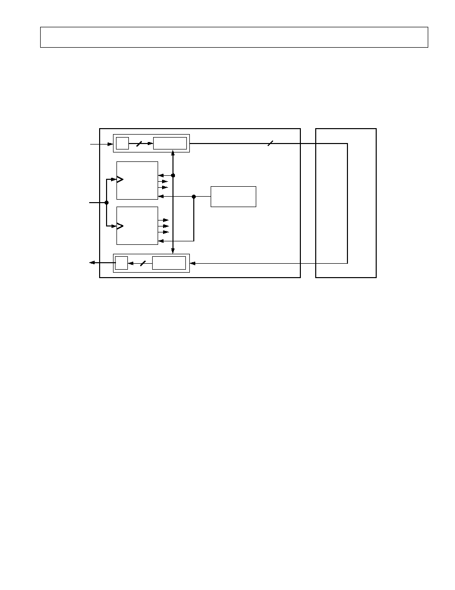
In V.32 Loopback Mode, shown in Figure 9, the AD28msp01's
receive circuitry and transmit circuitry are locked together.
RCONV is generated internally and can be phase adjusted with
the Receive Phase Adjust Register (Control Register 4). RBIT,
RBAUD, TCONV, TBIT and TBAUD are all locked to
RCONV.
RCONV initiates a new DAC sample update and loads Data
Register 2 with a new sample. The RCONV rate can be set to
9.6 kHz, 8.0 kHz or 7.2 kHz by setting the sample rate bit field
in Control Register 0. The bit and baud rates can be set to
any combination of clock rates listed in the control register
descriptions.
Figure 9. Loopback Mode Block Diagram
AD28msp01
A/D
DATA
REGISTER 2
CONTROL
REGISTER 4
RX PHASE ADJUST
ANALOG IN
MCLK
16
16
DSP Processor
D/A
DATA
REGISTER 0
16
ANALOG OUT
TCONV
TBIT
TBAUD
PHASE ADJUST
TX CLOCKS
TX CLOCKS
RCONV
RBIT
RBAUD
PHASE ADJUST
CONVERT
START
RX CLOCKS
V.32ter TSYNC Mode
This mode is identical to V.32 TSYNC Mode except all clocks
are scaled by a factor of 8/7 over the corresponding V.32
TSYNC rate. In this mode, the maximum value to which the re-
ceive and transmit phase adjust registers (Control Registers 4
and 5) may be set is +192.
Both TBIT and RBIT can be set to a 19,200 Hz rate that will
not be scaled by a factor of 8/7, by setting the appropriate fields
in Control Registers 2 and 3.
V.32ter Internal Sync Mode
This mode is identical to V.32 TSYNC Mode except all clocks
are scaled by a factor of 8/7 over the corresponding V.32
TSYNC rate. In this mode, the maximum value to which the
phase adjust registers (Control Registers 4 and 5) may be set is
+192.
Both TBIT and RBIT can be set to a 19,200 Hz rate that will
not be scaled by a factor of 8/7, by setting the appropriate fields
in Control Registers 2 and 3.
AD28msp01
REV. A
14
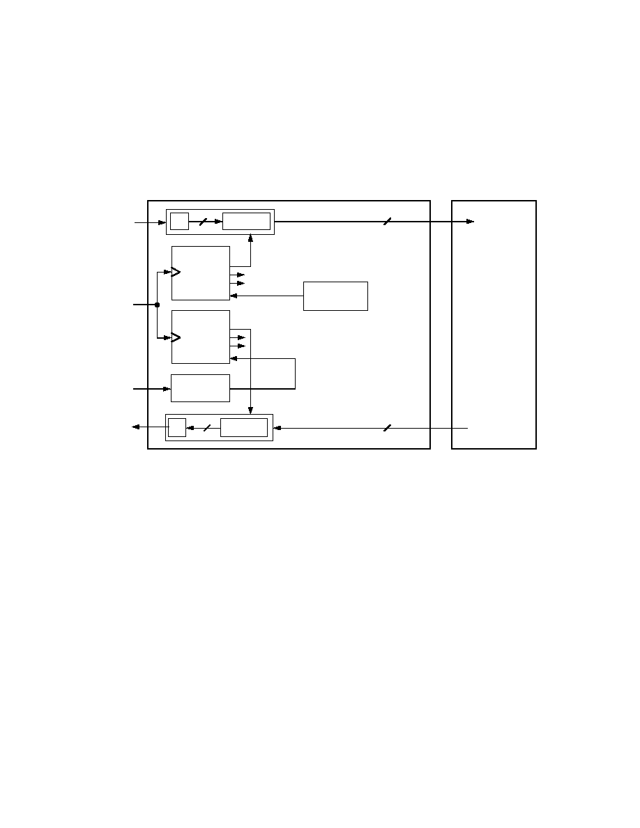
Asynchronous Fallback TSYNC Mode
The Asynchronous Fallback TSYNC Mode is shown in Figure
10. TCONV, TBIT and TBAUD are generated internally but
phase locked to the external TSYNC input signal. RCONV,
RBIT and RBAUD are generated internally and can be phase
adjusted with the Receive Phase Adjust Register (Control
Register 4).
This mode is entered by setting the Operating Mode field in
Control Register 0. The RCONV/TCONV rate can be set to
9.6 kHz, 8.0 kHz or 7.2 kHz by setting the sample rate bit field
in Control Register 0. The TBIT and TBAUD clock rates are
set by adjusting the appropriate bits in Control Register 3. The
RBIT and RBAUD clock rates are set by adjusting the appropri-
ate bits in Control Register 2. The bit rates, baud rates and
TSYNC rate can be set to any combination of clock rates listed
in the control register descriptions.
AD28msp01
A/D
DATA
REGISTER 2
CONTROL
REGISTER 4
RX PHASE ADJUST
ANALOG IN
MCLK
16
16
DSP Processor
D/A
DATA
REGISTER 0
16
ANALOG OUT
TCONV
TBIT
TBAUD
PHASE ADJUST
TX CLOCKS
TX CLOCKS
RCONV
RBIT
RBAUD
PHASE ADJUST
CONVERT
START
RX CLOCKS
DIGITAL PHASE
LOCKED LOOP
TSYNC
FROM MODEM TX
TO MODEM RX
16
Figure 10. Asynchronous Fallback TSYNC Driven Mode Block Diagram
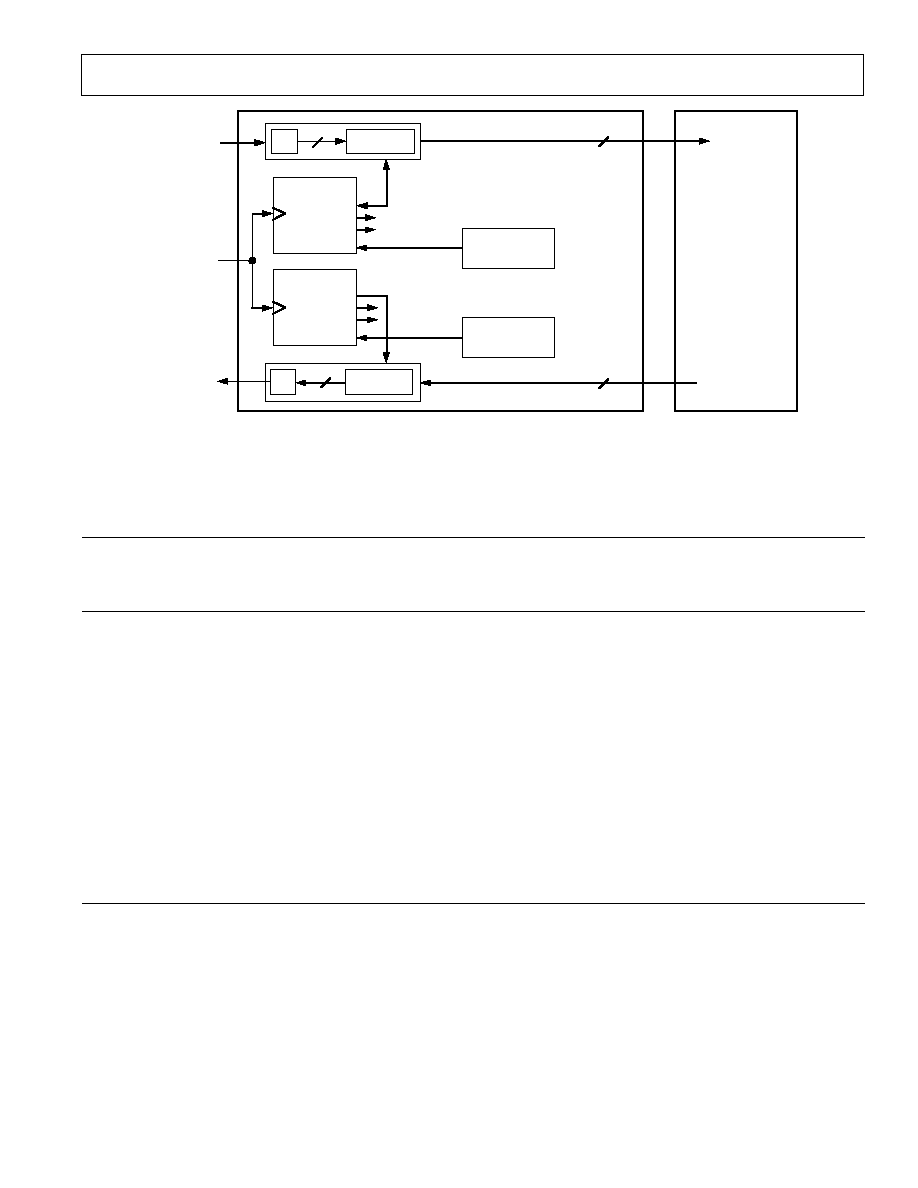
Asynchronous Fallback Mode
The Asynchronous Fallback Mode is shown in Figure 11.
TCONV, TBIT and TBAUD are generated internally and can
be phase adjusted with the Transmit Phase Adjust Register
(Control Register 5). RCONV, RBIT and RBAUD are gener-
ated internally and can also be phase adjusted with the Receive
Phase Adjust Register (Control Register 4). The digital phase-
locked is not used in this operating mode.
This mode is entered by setting the Operating Mode field in
Control Register 0. The RCONV/TCONV rate can be set to
9.6 kHz, 8.0 kHz or 7.2 kHz by setting the sample rate bit field
in Control Register 0. The TBIT and TBAUD clock rates are
set by adjusting the appropriate bits in Control Register 3. The
RBIT and RBAUD clock rates are set by adjusting the appropri-
ate bits in Control Register 2. The bit and baud rates can be set
to any combination of clock rates listed in the control register
descriptions.
AD28msp01
REV. A
15
FROM MODEM TX
TO MODEM RX
AD28msp01
A/D
DATA
REGISTER 2
CONTROL
REGISTER 4
RX PHASE ADJUST
ANALOG IN
MCLK
16
16
DSP Processor
D/A
DATA
REGISTER 0
16
ANALOG OUT
TCONV
TBIT
TBAUD
PHASE ADJUST
TX CLOCKS
TX CLOCKS
RCONV
RBIT
RBAUD
PHASE ADJUST
CONVERT
START
RX CLOCKS
FROM MODEM TX
TO MODEM RX
CONVERT
START
CONTROL
REGISTER 5
TX PHASE ADJUST
16
Figure 11. Asynchronous Fallback Mode Block Diagram
Operating Mode Summary
Table III summarizes the operating modes.
Table III. Operating Mode Summary
Internal Filter
Initial Phase
Phase Adjust
Operation
Control
Lock After
Normal DPLL* Register
Resampling
Synchronous To:
Register 0
Mode
Entering Mode
Operation
Programmable
Interpolator
ADC
DAC
OP 2-0
Async Fallback
no phase lock
no phase lock
RCV, TX
not used
RCONV
TCONV
0 0 0
Async TSYNC
TCONV lock
TCONV lock
RCV
not used
RCONV
TCONV
1 1 1
to TSYNC
to TSYNC
V.32 TSYNC
RCONV lock
TCONV lock
RCV
Input synchronous
TCONV
TCONV
1 0 0
to TCONV
to TSYNC
and in phase with
TCONV, Output
synchronous and in
phase with RCONV
V.32 Internal Sync RCONV lock
no phase lock
RCV, TX
Input synchronous
TCONV
TCONV
1 0 1
to TCONV
and in phase with
TCONV, Output
synchronous and in
phase with RCONV
V.32 Loopback
TCONV lock
no phase lock
RCV
not used
TCONV
TCONV
1 1 0
to RCONV
NOTES
*DPLL--Digital Phase-Locked loop.
RCV phase adjusted via Control Register 4, TX phase adjusted via Control Register 5.
Adjusting RCV phase also adjusts TX phase in this mode.
Note: All receive clocks: RBIT, RBAUD are synchronous to RCONV. All transmit clocks: TBIT, TBAUD are synchronous to TCONV.
AD28msp01
REV. A
16
DESIGN CONSIDERATIONS
Analog Input
The analog input signal to the AD28msp01 must be ac coupled.
Figure 12 shows the recommended input circuit for the
AD28msp01's analog input pin (V
IN
). The circuit of Figure 12
implements a first-order low-pass filter with a 3 dB point at
20 kHz; this is the only filter that must be implemented external
to the AD28msp01 to prevent aliasing of the sampled signal.
Since the AD28msp01's ADC uses a highly oversampled ap-
proach that transfers the bulk of the anti-aliasing filtering into
the digital domain, the off-chip anti-aliasing filter need only be
of low order.
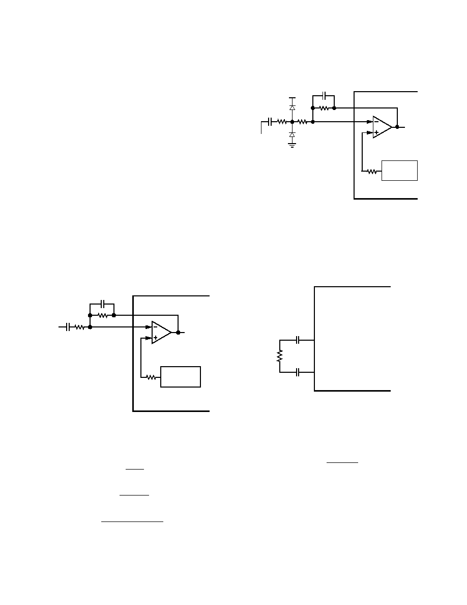
In the circuit shown in Figure 12, scaling of the analog input is
achieved by the resistors R
IN
and R
FB
. The input signal gain,
R
FB
/R
IN
, can be adjusted by varying the values of these resis-
tors. Total gain must be configured to ensure that a full-scale in-
put signal (at C
IN
in Figure 12) produces a signal level at the
input to the sigma-delta modulator of the ADC that does not
exceed V
INMAX
, which is specified under "Analog Interface Elec-
trical Characteristics." If the total gain is increased above unity
(i.e., gain >1), signal-to-noise (SNR + THD) performance may
not meet the listed specifications.
The dc offsetting of the analog input signal is accomplished with
an on-chip voltage reference which nominally equals 2.5 V. The
input signal must be ac coupled with an external coupling ca-
pacitor (C
IN
). C
IN
and R
IN
should be chosen to ensure a cou-
pling corner frequency of 30 Hz. C
IN
should be 0.1
µ
F or larger.
VOLTAGE
REFERENCE
AD28msp01
C
FB
C
IN
INPUT
SIGNAL
R
IN
R
FB
V
FB
V
IN
Figure 12. Recommended Analog Input Circuit
To select values for the components shown in Figure 12, use the
following equations:
Gain
=
R
FB
R
IN
C
IN
=
1
60
R
IN
C
FB
=
1
(2
)(20 *10
3
) R
FB
10 k
R
FB
, R
IN
50 k
150 pF
C
FB
600 pF
Figure 13 shows an example of a typical input circuit configured
for 0 dB gain. The circuit's diodes are used to prevent the input
signal from exceeding maximum limits.
INPUT
SIGNAL
10k
1.0
µ
F
V
CC
10k
20k
330pF
GND
A
VOLTAGE
REFERENCE
AD28msp01
V
FB
V
IN
Figure 13. Typical Input Circuit (0 dB Gain)
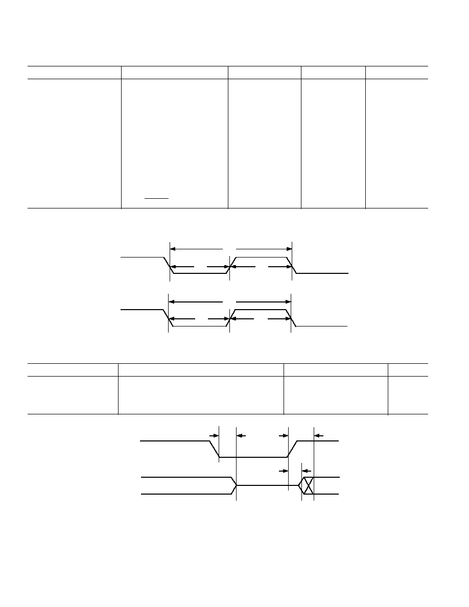
Analog Output
The AD28msp01's differential analog output (V
OUTP
, V
OUTN
) is
produced by an on-chip differential amplifier. The differential
amplifier can drive a minimum load of 2 k
(R
L
2 k
) and
has a maximum differential output voltage swing of 6.312 V
peak-to-peak (3.17 dBm0). The differential output can be ac-
coupled directly to a load or dc-coupled to an external amplifier.
AD28msp01
V
OUTP
V
OUTN
C
OUT
C
OUT
R
L
Figure 14. Example Circuit for Differential Output with AC
Coupling
Figure 14 shows a simple circuit providing a differential output
with ac coupling. The capacitor of this circuit (C
OUT
) is op-
tional; if used, its value can be chosen as follows:
C
OUT
=
1
(60
) R
L
The V
OUTP
V
OUTN
outputs must be used as differential outputs;
do not use either as a single-ended output. Figure 15 shows an
example circuit which can he used to convert the differential
output to a single-ended output. The circuit uses a differential-
to-single-ended amplifier, the Analog Devices SSM2141.
AD28msp01
REV. A
17
V
OUTP
V
OUTN
12V
4
7
SSM-214
GND
A
SSM2141
5
1
V
OUT
0.1
µ
F
GND
A
+12V
AD28msp01
0.1
µ
F
GND
A
Figure 15. Example Circuit for Single-Ended Output
Single Power Supply Operation
Use of a single +5 V power supply is possible with the
AD28msp01. If a single supply is used, the analog power supply
input to the device must be properly filtered. The proper filter is
dependent on the noise present in your system.
PC Board Layout Considerations
Separate analog and digital ground planes should be provided
for the AD28msp01 in order to assure the characteristics of the
device's ADC and DAC. The two ground planes should be con-
nected only at a single point. The point of connection may be at
the system power supply, at the PC board power connection, or
at any other appropriate location. Multiple connections between
the analog and digital ground planes should be avoided.
The ground planes should be designed such that all noise-
sensitive areas are isolated from one another and critical signal
traces (such as digital clocks and analog signals) are as short as
possible.
Each +5 V supply pin of the AD28msp01 should be bypassed to
ground with a 0.1
µ
F capacitor. These capacitors should be low
inductance, monolithic, ceramic, and surface-mount. The ca-
pacitor leads and PC board traces should be as short as possible
to minimize inductive effects. In addition, a 10
µ
F capacitor
should be connected between V
DD
and ground, near the PC
board power connection.
MCLK Frequency
The sigma-delta converters and digital filters of the AD28msp01
are specifically designed to operate at a master clock (MCLK)
frequency of 13.824 MHz. MCLK must equal 13.824 MHz to
guarantee the filter characteristics and sample rate of the ADC
and DAC. The AD28msp01 is not tested or characterized at
any other clock frequency.
DEFINITION OF SPECIFICATIONS
Typical (Typ) specifications represent nominal performance at
+25
°
C with V
CC
and V
DD
set to +5 V.
Minimum (Min) and Maximum (Max) specifications are guar-
anteed across the full operating range, however, devices are
tested only at the indicated test conditions.
Absolute Gain
Absolute gain is a measure of converter gain for a known signal.
Absolute gain is measured with a 1.0 kHz sine wave at 0 dBm0.
The absolute gain specification is used as a reference for gain
tracking error specification.
Gain Tracking Error
Gain tracking error measures changes in converter output for
different signal levels relative to an absolute signal level. The ab-
solute signal level is 1 kHz at 0 dBm0 (equal to absolute gain).
Gain tracking error at 0 dBm0 is 0 dB by definition.
SNR
Signal-to-noise ratio is defined to be the ratio of the rms value of
the measured input signal to the rms sum of all the spectral
components in the specified passband, excluding dc and har-
monic components.
THD
Total harmonic distortion is defined to be the ratio of the rms
value of the measured input signal to the rms sum of the har-
monic components in the specified passband.
Intermodulation Distortion
With inputs consisting of sine waves at two frequencies, f
a
and
f
b
, any active device with nonlinearities will create distortion
products at sum and difference frequencies of mf
a
±
nf
b
where
m, n = 0, 1, 2, 3, etc. Intermodulation terms are those for which
neither m nor n are equal to zero. This specification contains
the second order terms include (f
a
+ f
b
) and (f
a
f
b
), and the
third order terms include (2f
a
+ f
b
), (2f
a
f
b
), (f
a
+ 2f
b
), and
(f
a
2f
b
).
Idle Channel Noise
Idle channel noise is defined as the total signal energy measured
at the output of the device when the input is grounded (mea-
sured in the specified passband).
Crosstalk
Crosstalk is defined as the ratio of the amplitude of a 0 dB sig-
nal appearing on one channel to the amplitude of the same sig-
nal coupled onto the other, idle channel. Crosstalk is expressed
in dB.
Power Supply Rejection
Power supply rejection measures the susceptibility of a device to
noise on the power supply. Power supply rejection is measured
by modulating the power supply with a 1 kHz, 100 mV p-p sine
wave and measuring the relative level at the output.
Group Delay
Group delay is defined as the derivative of radian phase with re-
spect to radian frequency,
()/
. Group delay is a measure
of the linearity of the phase response of a linear system. A linear
system with a constant group delay has a linear phase response.
The deviation of the group delay away from a constant indicates
the degree of nonlinear phase response of the system.

AD28msp01SPECIFICATIONS
RECOMMENDED OPERATING CONDITIONS
K Grade
Symbol
Parameter
Min
Max
Unit
V
DD
, V
CC
Supply Voltage
4.75
5.25
V
T
AMB
Ambient Operating Temperature
0
+70
°
C
Refer to Environmental Conditions for information on case temperature and thermal specifications.
REV. A
18
ESD SENSITIVITY
The AD28msp01 features proprietary input protection circuitry to dissipate high-energy discharges
(Human Body Model). Per Method 3015 of MIL-STD-883 the AD28msp01 has been classified as a
Class 1 device.
Proper ESD precautions are strongly recommended to avoid functional damage or performance
degradation. Charges readily accumulate on the human body and test equipment and discharge without
detection. Unused devices must be stored in conductive foam, trays, or tubes, and the foam should be
discharged to the destination socket before devices are removed.
WARNING!
ESD SENSITIVE DEVICE
ABSOLUTE MAXIMUM RATINGS*
Supply Voltage . . . . . . . . . . . . . . . . . . . . . . . . . 0.3 V to +7 V
Input Voltage . . . . . . . . . . . . . . . . . . . . 0.3 V to V
DD
+ 0.3 V
Output Voltage Swing . . . . . . . . . . . . . 0.3 V to V
DD
+ 0.3 V
Operating Temperature Range (Ambient) . . . . . 0
°
C to +70
°
C
Storage Temperature Range . . . . . . . . . . . . 55
°
C to +150
°
C
Lead Temperature (5 seconds) SOIC . . . . . . . . . . . . +280
°
C
*Stresses above those listed under "Absolute Maximum Ratings" may cause
permanent damage to the device. These are stress rating only and functional
operation of the device at these or any other conditions above those indicated in
the operational sections of this specification is not implied. Exposure to absolute
maximum rating conditions for extended periods may affect device reliability.
Test Conditions Unless Otherwise Noted
Temperature
+25
°
C
Sample Rate (F
S
)
9.6 kHz
Input Signal Frequency
993.75 Hz
Input Signal Level
0.0 dBm0
Analog Input Gain
Unity
Analog Output Passband
220 Hz to 3.4 kHz

AD28msp01
REV. A
19
DIGITAL INTERFACE ELECTRICAL CHARACTERISTICS
Symbol
Parameter
Min
Typ
Max
Unit
Test Condition
V
IH
Input High Voltage
2.4
V
V
DD
= max
V
IL
Input Low Voltage
0.8
V
V
DD
= min
V
OH
Output High Voltage
2.4
V
V
DD
= min, I
OH
= 0.5 mA
V
OL
Output Low Voltage
0.4
V
V
DD
= min, I
OL
= 2 mA
I
IH
High Level Input Current
10
µ
A
V
DD
= max, V
IN
= max
I
IL
Low Level Input Current
10
µ
A
V
DD
= max, V
IN
= 0 V
I
OZL
Low Level Output 3-State Leakage Current
10
µ
A
V
DD
= max, V
IN
= max
I
OZH
High Level Output 3-State Leakage Current
10
µ
A
V
DD
= max, V
IN
= 0 V
C
I
Digital Input Capacitance
1
10
pF
1
Guaranteed but not tested.
ANALOG INTERFACE ELECTRICAL CHARACTERISTICS
Symbol
Parameter
Min
Typ
Max
Unit
ADC:
I
L
Input Leakage Current at V
IN
10
nA
R
I
Input Resistance at V
IN
100
M
C
IL
Input Load Capacitance at V
FB
10
pF
VIN
MAX
Maximum Input Range
1
3.156
V p-p
DAC:
Ro
Output Resistance
1
V
OFF
Output DC Offset
2
400
400
mV
C
OL
Output Load Capacitance
100
pF
V
O
Maximum Voltage Output Swing (p-p) Across R
L
Single-Ended
3.156
V
Differential
6.312
V
R
L
Load Resistance
2
k
Test Conditions for all analog interface tests: Unity input gain, no load on analog output (V
OUTP
V
OUTN
).
1
At unity gain on input.
2
Between V
OUTP
and V
OUTN
.
POWER DISSIPATION
Symbol
Parameter
Min
Typ
Max
Unit
V
CC
Analog Operating Voltage
4.75
5.0
5.25
V
V
DD
Digital Operating Voltage
4.75
5.0
5.25
V
I
CC
Analog Operating Current Active
1
24
35
mA
I
DD
Digital Operating Current Active
1
11
20
mA
P
1
Power Dissipation Active'
350
mW
I
CC
Analog Operating Current Inactive
2
300
µ
A
I
DD
Digital Operating Current Inactive
2
200
µ
A
P
0
Power Dissipation Inactive
2
4.0
mW
Test conditions: V
DD
= V
CC
= 5.0 V, MCLK frequency 13.824 MHz, no load on digital pins, analog inputs ac-coupled to ground, no load on analog output
(V
OUTP
V
OUTN
).
1
Active: AD28msp01 operational (PWDD and PWDA set to 1 in Control Register 1).
2
Inactive: AD28msp01 in power-down state (PWDD and PWDA set to 0 in Control Register 1) and MCLK tied to V
DD
.
AD28msp01
REV. A
20
TIMING PARAMETERS
Parameter
Min
Max
Unit
Clock Signals
Timing Requirement:
F
MCK
MCLK Frequency
13.824
13.824
MHz
±
50 ppm
t
MCK
MCLK Period
72.34
72.34
ns
t
MKL
MCLK Width Low
0.5t
MCK
10
0.5t
MCK
+ 10
ns
t
MKH
MCLK Width High
0.5t
MCK
10
0.5t
MCK
+ 10
ns
Switching Characteristic:
t
SCK
SCLK Period
8t
MCK
10
8t
MCK
+ 10
ns
t
SKL
SCLK Width Low
4t
MCK
10
4t
MCK
+ 10
ns
t
SKH
SCLK Width High
4t
MCK
10
4t
MCK
+ 10
ns
Control Signals
Timing Requirement:
t
RSP
RESET
Width Low
5t
MCK
1
ns
NOTE
1
Applies after power-up sequence is complete. Internal phase lock loop requires no more than 1000 processor cycles assuming stable CLKIN (not including
crystal oscillator start-up time).
MCLK
SCLK
t
MCK
t
MKL
t
MKH
t
SKH
t
SCK
t
SKL
Figure 16. Clock Signals
Serial Port 3-State
Parameter
Min
Max
Unit
Switching Characteristic:
t
SPD
CS Low to SDO, SDOFS, SCLK Disable
20
ns
t
SPE
CS High to SDO, SDOFS, SCLK Enable
0
ns
t
SPV
CS High to SDO, SDOFS, SCLK Valid
25
ns
CS
t
SPD
t
SPV
t
SPE
SDO
SDOFS
SCLK
Figure 17. Serial Port 3-State
AD28msp01
REV. A
21
Output Disable Time
Output pins are considered to be disabled when they have
stopped driving and started a transition from the measured out-
put high or low voltage to a high-impedance state. The output
disable time (t
DIS
) is the difference of t
MEASURED
and t
DECAY
, as
shown in the Output Enable/Disable diagram. The time,
t
MEASURED
, is the interval from when a reference signal reaches a
high or low voltage level to when the output voltages have
changed by 0.5 V from the measured output high or low volt-
age. The decay time, t
DECAY
, is dependent on the capacitive
load, C
L
, and the current load, i
L
, on the output pin. It can be
approximated by the following equation:
t
DECAY
=
C
L
×
0.5 V
i
L
from which
t
DIS
= t
MEASURED
t
DECAY
is calculated. If multiple pins (such as the data bus) are dis-
abled, the measurement value is that of the last pin to stop
driving.
Output Enable Time
Output pins are considered to be enabled when they have made
a transition from a high-impedance state to when they start driv-
ing. The output enable time (t
ENA
) is the interval from when a
reference signal reaches a high or low voltage level to when the
output has reached a specified high or low trip point, as shown
in the Output Enable/Disable diagram. If multiple pins (such as
the data bus) are enabled, the measurement value is that of the
first pin to start driving.
V
+ 0.5V
OL
(MEASURED)
V
OH
0.5V
(MEASURED)
REFERENCE
SIGNAL
OUTPUT
V
OH
(MEASURED)
HIGH-IMPEDANCE STATE. TEST CONDITIONS CAUSE THIS
VOLTAGE LEVEL TO BE APPROXIMATELY 1.5 V.
t
ENA
OUTPUT STOPS
DRIVING
OUTPUT STARTS
DRIVING
MEASURED
t
2.0V
1.0V
DECAY
t
OH
(MEASURED)
V
(MEASURED)
OL
V
t
DIS
V
OL
(MEASURED)
Figure 18. Output Enable/Disable
Serial Ports
Parameter
Min
Max
Unit
Timing Requirement:
t
SCS
SDI/SDIFS Setup before SCLK Low
10
ns
t
SCH
SDI/SDIFS Hold after SCLK Low
15
ns
Switching Characteristic:
t
RD
SDOFS Delay from SCLK High
30
ns
t
RH
SDOFS Hold after SCLK High
0
ns
t
SCDH
SDO Hold after SCLK High
0
ns
t
SCDD
SDO Delay from SCLK High
30
ns
SCLK
SDIFS
SDI
MSB
2ND MSB
3RD MSB
SDOFS
SDO
t
RD
t
SCS
t
SCH
t
SCK
t
RH
t
SCDD
t
SCS
t
SCH
t
SCDH
Figure 19. Serial Ports
AD28msp01
REV. A
22
DIGITAL TEST CONDITIONS
3.0V
1.5V
0.0V
2.0V
1.5V
0.8V
DIGITAL INPUT
DIGITAL OUTPUT
Figure 20. Voltage Reference Levels for AC Measurements
(Except Output Enable/Disable)
50pF
+
1.5V
I
OL
I
OH
TO DIGITAL
OUTPUT PIN
Figure 21. Equivalent Device Loading for AC Measurements
(Includes ALI Fixtures)
GAIN
Parameter
Min
Typ
Max
Unit
Test Conditions
ADC Absolute Gain
0.5
0
0.5
dBm0
1.0 kHz, 0 dBm0
ADC Gain Tracking Error
0.1
0
0.1
dBm0
1.0 kHz, +3 and 60 dBm0
DAC Absolute Gain
0.5
0
0.5
dBm0
1.0 kHz, 0 dBm0
DAC Gain Tracking Error
0.1
0
0.1
dBm0
1.0 kHz, +3 and 60 dBm0
FREQUENCY RESPONSE*
ADC
9.6 kHz
8.0 kHz
7.2 kHz
Passband Ripple
<0.2 dB
<0.2 dB
<0.2 dB
Low-Pass Passband Cutoff Frequency
3.4 kHz
3.4 kHz
3.3 kHz
Low-Pass Stopband Cutoff Frequency
4.8 kHz
4.0 kHz
3.6 kHz
High-Pass Passband Cutoff Frequency
220 Hz
220 Hz
220 Hz
High-Pass Stopband Cutoff Frequency
60 Hz
60 Hz
60 Hz
Low-Pass Stopband Rejection
50 dB
50 dB
50 dB
High-Pass Stopband Rejection
50 dB
50 dB
50 dB
DAC
9.6 kHz
8.0 kHz
7.2 kHz
Passband Ripple
<0.2 dB
<0.2 dB
<0.2 dB
Passband Cutoff Frequency
3.4 kHz
3.4 kHz
3.4 kHz
Low-Pass Stopband Cutoff Frequency
4.8 kHz
4.0 kHz
3.6 kHz
Stopband Rejection
50 dB
50 dB
50 dB
*Frequency Response is guaranteed but not tested.
AD28msp01
REV. A
23
NOISE AND DISTORTION
Parameter
Min
Typ
Max
Unit
ADC Signal-to-Noise Ratio
+72
+80
dB
ADC Total Harmonic Distortion
72
dB
DAC Signal-to-Noise Ratio
+72
+80
dB
DAC Total Harmonic Distortion
72
dB
ADC Idle Channel Noise
80
72
dBm0
DAC Idle Channel Noise
80
72
dBm0
ADC Crosstalk
1
72
dB
DAC Crosstalk
1
72
dB
ADC Intermodulation Distortion
1
dB
DAC Intermodulation Distortion
1
72
dB
ADC Digital Power Supply Rejection
1
45
dB
DAC Digital Power Supply Rejection
1
45
dB
ADC Analog Power Supply Rejection
1
35
dB
DAC Analog Power Supply Rejection
1
35
dB
1
Guaranteed but not tested
V
IN
dBm0
SNR dB
17dB
80
10
3.17
10
0
55
60
20
30
40
50
60
70
0
5
10
15
20
30
35
40
45
50
25
Figure 22. Typical SNR vs. V
IN
GROUP DELAY*
9.6 kHz
8.0 kHz
7.2 kHz
Unit
ADC Group Delay
12
13
15
ms
ADC Low-Pass Filter Group Delay
2
3
5
ms
ADC High-Pass Filter Group Delay
10
10
10
ms
DAC Group Delay
2
3
5
ms
Resampling Filter Group Delay
2
3
5
ms
*Group Delay is guaranteed but not tested.
AD28msp01
REV. A
24
PIN CONFIGURATIONS
28-Pin DIP and 28-Lead SOIC
1
2
3
7
28
27
26
22
8
9
10
21
20
19
11
12
18
17
4
5
25
24
6
23
TOP VIEW
(Not to Scale)
13
14
16
15
AD28msp01
V
CC
V
OUTP
V
OUTN
V
CC
NC
GND
A
GND
A
GND
D
GND
D
RESET
NC
TSYNC
TCONV
NC
NC = NO CONNECT
NC
GND
D
GND
D
GND
A
V
IN
V
FB
CS
SDI
SDIFS
SDOFS
SDO
SCLK
V
DD
V
DD
44-Lead Plastic Leaded Chip Carrier (PLCC)
AD28msp01
(Not to Scale)
TOP VIEW
2
1
44
3
4
5
6
42
41
40
43
18
19
20
21
22
23
24
25
26
27
28
39
38
37
36
35
34
33
32
31
30
29
7
8
9
10
11
12
13
14
15
16
17
14
V
CC
V
CC
V
DD
V
OUTP
V
OUTN
NC
GND
A
NC
GND
A
NC
V
FB
V
IN
RBIT
MCLK
RBAUD
GND
D
RCONV
SCLK
NC
GND
D
GND
A
GND
D
CS
NC
SDI
SDIFS
NC
SDOFS
SDO
NC
GND
A
GND
D
RESET
NC
TSYNC
TCONV
NC
TBIT
TBAUD
NC
GND
D
NC = NO CONNECT
GND
D
V
DD
V
DD
AD28msp01
REV. A
25
44-Lead Thin Quad Flat Pack
GND
A
11
12
23
22
1
44
34
33
TOP VIEW
(Pins Down)
GND
D
GND
D
CS
NC
SDI
SDIFS
NC
SDOFS
SDO
NC
GND
A
GND
D
GND
D
NC
TSYNC
TCONV
NC
TBIT
TBAUD
NC
GN
D
A
NC
V
OU
T
N
V
OU
T
P
V
CC
V
CC
NC
V
IN
V
FB
NC
GN
D
A
RCO
NV
RBIT
RBAUD
MC
L
K
GN
D
D
GN
D
D
V
DD
V
DD
V
DD
NC
SC
L
K
NC = NO CONNECT
RESET
OUTLINE DIMENSIONS
Dimensions shown in inches and (mm).
N-28
28-Pin Plastic DIP
28
1
14
15
1.450 (36.830)
1.440 (35.580)
0.550 (13.970)
0.530 (13.470)
PIN 1
0.020 (0.508)
0.015 (0.381)
0.060 (1.580)
0.020 (0.508)
0.175 (4.450)
0.120 (3.050)
SEATING
PLANE
0.200
(5.080)
MAX
0.105 (2.670)
0.096 (2.420)
0.012 (0.306)
0.008 (0.203)
0.606 (15.400)
0.594 (15.090)
15°
0°
AD28msp01
REV. A
26
P-44A
44-Lead Plastic Leaded Chip Carrier (PLCC)
6
PIN 1
IDENTIFIER
7
40
39
17
18
29
28
TOP VIEW
(PINS DOWN)
0.695 (17.65)
0.685 (17.40)
SQ
0.656 (16.66)
0.650 (16.51)
SQ
0.048 (1.21)
0.042 (1.07)
0.048 (1.21)
0.042 (1.07)
0.020
(0.50)
R
0.021 (0.53)
0.013 (0.33)
0.050
(1.27)
BSC
0.63 (16.00)
0.59 (14.99)
0.032 (0.81)
0.026 (0.66)
0.180 (4.57)
0.165 (4.19)
0.040 (1.01)
0.025 (0.64)
0.025 (0.63)
0.015 (0.38)
0.110 (2.79)
0.085 (2.16)
0.056 (1.42)
0.042 (1.07)
R-28
28-Lead Wide-Body SOIC
28
15
14
1
0.7125 (18.10)
0.6969 (17.70)
0.4193 (10.65)
0.3937 (10.00)
0.2992 (7.60)
0.2914 (7.40)
PIN 1
SEATING
PLANE
0.0118 (0.30)
0.0040 (0.10)
0.0192 (0.49)
0.0138 (0.35)
0.1043 (2.65)
0.0926 (2.35)
0.0500
(1.27)
BSC
0.0125 (0.32)
0.0091 (0.23)
0.0500 (1.27)
0.0157 (0.40)
8
°
0
°
0.0291 (0.74)
0.0098 (0.25)
x 45
°
AD28msp01
REV. A
27
ST-44
44-Lead Metric Thin Plastic Quad Flat Pack (TQFP)
SEATING
PLANE
0.063 (1.60)
MAX
0.030 (0.75)
0.019 (0.50)
0.004
(0.10)
MAX
0.057 (1.45)
0.053 (1.35)
0.006 (0.15)
0.002 (0.05)
TOP VIEW
(PINS DOWN)
1
33
34
44
11
12
23
22
0.640 (16.25)
0.620 (15.75)
0.553 (14.05)
0.549 (13.95)
0.397 (10.07)
0.391 (9.93)
0.553 (14.05)
0.549 (13.95
0.397 (10.07)
0.391 (9.93)
0.640 (16.25)
0.620 (15.75)
0.016 (0.40)
0.012 (0.30)
0.042 (1.07)
0.037 (0.93)
ORDERING GUIDE
Part Number
Temperature Range
Package
Package Option*
AD28msp01KP
0
°
C to +70
°
C
44-Pin PLCC
P-44A
AD28msp01KN
0
°
C to +70
°
C
28-Pin Plastic DIP
N-28
AD28msp01KR
0
°
C to +70
°
C
28-Lead SOIC
R-28
AD28msp01KST
0
°
C to +70
°
C
44-Lead TQFP
ST-44
NOTES
*P = PLCC, N = Plastic DIP, R = Small Outline (SOIC), ST = TQFP.
In Development.

C1726a48/93
PRINTED IN U.S.A.
28
Document Outline
- Specifications
- Pinout
- Package drawings
- Ordering Guide
- Features
- Applications
- Product Description
- Absolute Maximum Ratings
- Functional Block Diagram
- PIN DESCRIPTIONS
- FUNCTIONAL DESCRIPTION
- D/A CONVERSION
- DAC
- SERIAL PORT
- DESIGN CONSIDERATIONS
- DEFINITION OF SPECIFICATIONS
- RECOMMENDED OPERATING CONDITIONS
- ESD SENSITIVITY
- DIGITAL INTERFACE ELECTRICAL CHARACTERISTICS
- ANALOG INTERFACE ELECTRICAL CHARACTERISTICS
- POWER DISSIPATION
- TIMING PARAMETERS
- DIGITAL TEST CONDITIONS
- GAIN
- FREQUENCY RESPONSE*
- NOISE AND DISTORTION
- GROUP DELAY*
- DIAGRAMS
- Block Diagram
- AD28msp01-to-DSP Processor Interface
- AD28msp01-to-ADSP-2101 Interface
- V.32 TSYNC Mode Block Diagram
- V.32 Internal Sync Mode Block Diagram
- Loopback Mode Block Diagram
- Asynchronous Fallback TSYNC Driven Mode Block Diagram
- Asynchronous Fallback Mode Block Diagram
- Recommended Analog Input Circuit
- Typical Input Circuit (0 dB Gain)
- Example Circuit for Single-Ended Output
- Clock Signals
- Serial Port 3-State
- Output Enable/Disable
- Serial Ports
- Voltage Reference Levels for AC Measurements
- Equivalent Device Loading for AC Measurements