 | ÐлекÑÑоннÑй компоненÑ: AD5011 | СкаÑаÑÑ:  PDF PDF  ZIP ZIP |
Äîêóìåíòàöèÿ è îïèñàíèÿ www.docs.chipfind.ru
REV PrA
Information furnished by Analog Devices is believed to be accurate and
reliable. However, no responsibility is assumed by Analog Devices for its
use, nor for any infringements of patents or other rights of third parties
which may result from its use. No license is granted by implication or
otherwise under any patent or patent rights of Analog Devices.
a
2 Pair/1 Pair ETSI Compatible
HDSL Analog Front End
Preliminary Technical Data
AD5011
One Technology Way, P.O. Box 9106, Norwood, MA 02062-9106, U.S.A.
Tel: 781/329-4700
Fax: 781/326-8703
World Wide Web Site: hppt://www.analog.com
FEATURES
Integrated front End for Single Pair or Two Pair HDSL
Systems
Meets ETSI Specifications
Supports 1168 kbps and 2.32 Mbps
Programmable Filtering Supports Adaptive HDSL
Transmit and Receive Signal Path Functions
Receive Hybrid Amplifier, PGA, ADC and Adaptable
Filter
Transmit DAC, Adaptable Filter and Differential
Outputs
Normal Loopback
Serial Interface to Digital Transceivers
Single 3 V Power Supply
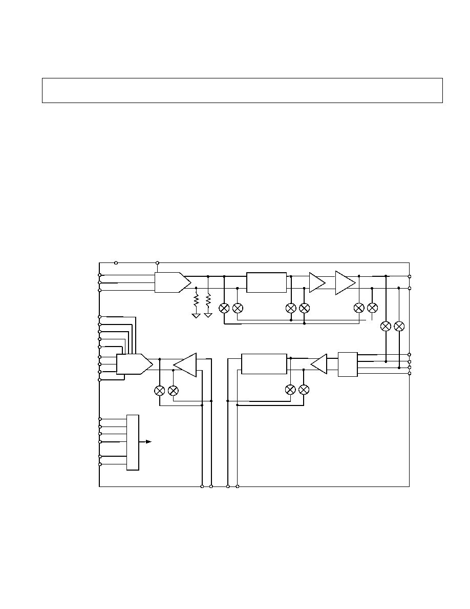
FUNCTIONAL BLOCK DIAGRAM
GENERAL DESCRIPTION
The AD5011 is an analog front end for two pair or single
pair HDSL applications that use 1168 kbps or 2.32 Mbps
data rates. The device integrates all the transmit and receive
functional blocks. A standard serial interface is used to
communicate with the DAC and ADC. The filters in both
the transmit and receive paths are programmable which
allows adaptive HDSL to be performed also. The part is
available in a 48-pin LQFP package and is specified for a
temperature range of -40
o
C to +85
o
C.
1 4-B it D A C
6 P ole A da ptive
B esse l Filte r
P G A
L in e
D rive r
H ybrid
P G A
4 P ole A da ptive
B utterw orth Filter
A D C
B uffer
1 2-B it A D C
S P I
S P IC LK
T FS
D T
D R
R E S E T B
P W R D O W N B
T xD A T A
T xS Y N C
T xC LK
A D C C LK
S C L K
S D O
D R
C A P -T
C A P -B
R E F -C O M
V R E F
T x-D E C O U P
D R V -O U T P
H Y B IN -2 B
AD
CI
NN
AD
CI
NP
FI
LO
U
T
P
FI
LO
U
T
N
0 dB
-6 dB
-6 dB
-3 dB
0 dB
+3 d B
+6 d B
D R V -O U T N
H Y B IN -2 A
H Y B IN -1 A
H Y B IN -1 B
V D R IV E
C M -L V L
C on trol/
C on figu ratio n
PRELIMINARY TECHNICAL DATA
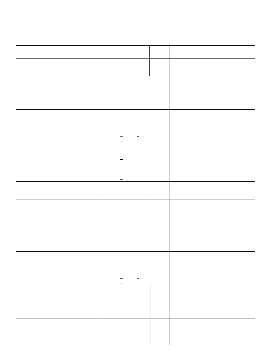
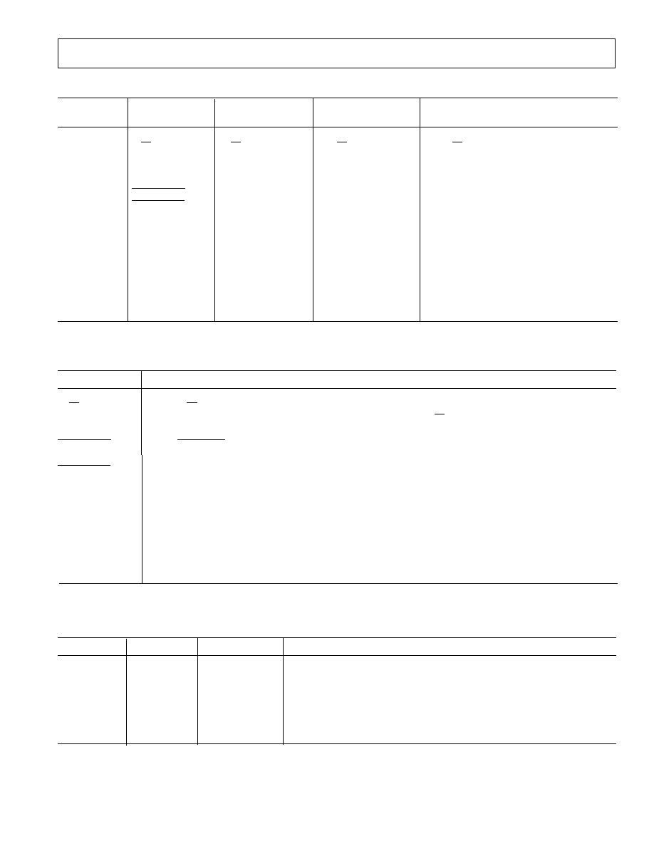
Parameter
AD5011B
Units
Test Conditions/Comments
Min
Typ
Max
TRANSMIT CHANNEL
Signal to Noise
2
68
71
dB
F
OUT
= 73 kHz
Total Harmonic Distortion
2
66
71
dB
F
OUT
= 73 kHz
TRANSMIT DAC
Resolution
14
Bits
Clock Frequency
18.688
MHz
Coding
2s Complement
Output Update Rate
3
1168
kHz
Output Voltage
1
Vpp Diff
TRANSMIT FILTER
Cutoff Frequency
4
49 - 120.8
kHz
Bottom Range (8 kHz steps)
108 - 265
kHz
Mid Range (18 kHz steps)
235 - 580
kHz
Top Range (40.5 kHz steps)
Corner Frequency Accuracy
+5
+10
%
Adjacent Corner Step
+40
% nom
LINE DRIVER
5
VCM
1.5
V
Common Mode Voltage Error
+100
mV
Output Power
13.5
dBm
Output Voltage
4
Vpp Diff
Tx-GAIN = 0
2
Vpp Diff
Tx-GAIN = 1
Channel Gain Accuracy
+1
dB
RECEIVE CHANNEL
Signal to (Noise + Distortion)
6
66
68
dB
F
IN
= 73 kHz
Total Harmonic Distortion
68
71
dB
F
IN
= 73 kHz
HYBRID INTERFACE
Input Voltage Range
5
Vpp Diff
PGA = 0 dB
Common Mode Input Voltage
1.5
V
Input Impedance
10
k
W
Input Offset Voltage
80
mV
PGA = 0 dB
PROGRAMMABLE GAIN AMPLIFIER
7
For all Gain Settings from -6 dB to +9 dB
Overall Gain Accuracy
+1
dB
Gain Step
3
dB
Gain Step Accuracy
+0.25
dB
RECEIVE FILTER
Cutoff Frequency
4
49 - 120.8
kHz
Bottom Range (8 kHz steps)
108 - 265
kHz
Mid Range (18 kHz steps)
235 - 580
kHz
Top Range (40.5 kHz steps)
Accuracy
+5
+10
%
Adjacent Corner Step
+40
% nom
Output Load Capacitance
20
pF
Output Load Resistance
TBD
W
RECEIVE ADC
Resolution
12
Bits
Coding
2s Complement
Sample Rate
2.32
MHz
LOGIC INPUTS
Input Logic High, V
INH
8
2
3
V
Input Logic Low, V
INL
0
0.2
V
I
IN
, Input Current
+10
m
A
V
IN
= 0 V to DVDD
C
IN
, Input Capacitance
10
pF
REV PrA
2
AD5011SPECIFICATIONS
1
(V
DD
= +3.15 V to +3.45 V; AGND = DGND = 0 V; T
A
= T
MIN
to T
MAX
unless otherwise
noted)
PRELIMINARY TECHNICAL DATA

AD5011
3
REV PrA
PRELIMINARY TECHNICAL DATA
Parameter
AD7346B
Units
Test Conditions/Comments
Min
Typ
Max
LOGIC OUTPUTS
Output Logic High, V
OH
9
VDD - 0.3
V
I
OUT
= 200
m
A
Output Logic Low, V
OL
0.3
V
I
OUT
= 200
m
A
POWER SUPPLIES
AVDD, DVDD
3.15
3.3
3.45
V
IDD
Normal Mode (excluding Driver)
32
mA
Line Driver
75
mA
33
W
Differential Load
1
Operating temperature range is as follows: B Version: 40°C to +85°C.
2
The complete transmit path spectrum and pulse shape comply with ETSI requirements. SNR and THD are measured within a 547 kHz bandwidth. Noise and Spurious
tones beyong 540 kHz are therefore excluded.
3
The transmit DAC maximum update rate is half the maximum output data rate i.e. 1168 kHz. The maximum transmit clock is 16 x 1168 = 18.688 MHz.
4
There are three ranges (bottom range, mid range, top range), each range being divided into eight steps. The transmit filter corner frequency can be set independently from
the receive filter corner frequency. the filter tuning circuit requires a continuous 16.384 MHz clock applied to the Fclk pin.
5
Transformer turns ratio = 1:2:3 at 50 kHz when loaded by ETSI (RTR/TM3036) HDSL test loops.
6
With 547 kHz filter snd 0 dB PGA gain selected.
7
The PGA gain is set by setting the PGA-GC bits in the control register.
8
The input switching threshold voltage is approximately 1.2 V to allow interfacing to 2.5 V and 3.3 V logic.
9
The output level is determined by the voltage on the logic supply pin V
DRIVE
.
Specifications subject to change without notice.
AD5011
4
REV PrA
PRELIMINARY TECHNICAL DATA
TIMING CHARACTERISTICS
(V
DD
= +2.7 V to +5.5 V; AGND = DGND = 0 V, unless otherwise noted)
Limit at
T
MIN
to T
MAX
Parameter
(B Version)
Units
Test Conditions/Comments
ADCCLK <= 1160kHz
t
1
1.5*t
3
ns min
ADCCLK Rising Edge to SCLK Rising Edge Delay
2*t
3
ns typ
t
2
2.5*t
3
ns min
SCLK Rising Edge to ADCCLK Falling Edge Delay
3*t
3
ns typ
t
3
26.939
ns min
SCLK Period (1/32*ADCCLK Period)
t
4
5
ns min
Data Setup Time Before SCLK Falling Edge
t
5
10
ns min
Data Hold Time After SCLK Falling Edge
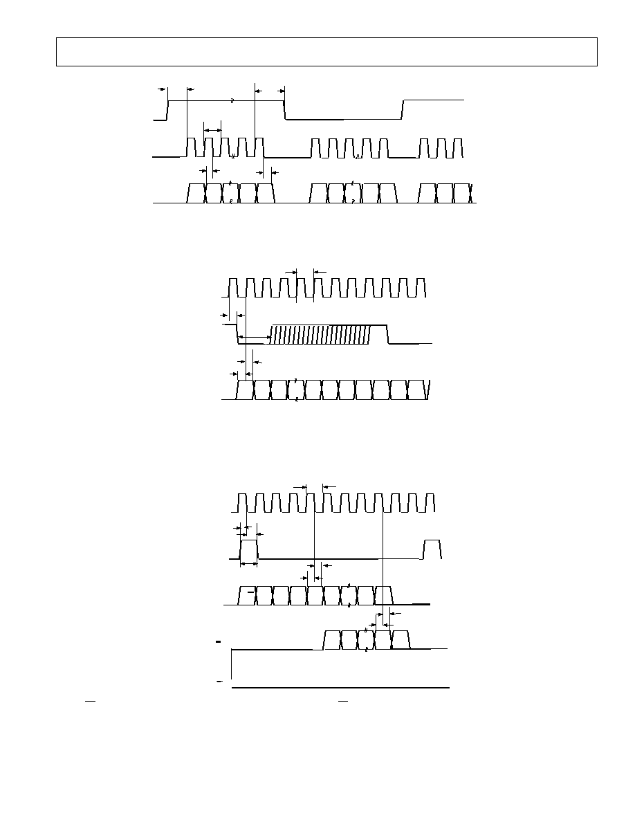
1160 kHz < ADCCLK <= 2320 kHz
t
6
20
ns min
ADCCLK Rising Edge to SCLK Rising Edge Delay
1*t
8
ns typ
t
7
1.5*t8
ns min
SCLK Rising Edge to ADCCLK Falling Edge Delay
2*t
8
ns typ
t
8
26.939
ns min
SCLK Period (1/16*ADCCLK Period)
t
9
5
ns min
Data Setup Time Before SCLK Falling Edge
t
10
10
ns min
Data Hold Time After SCLK Falling Edge
TRANSMIT DAC
t
11
53.5
ns min
TxCLK Period (1/18.688 MHz)
t
12
12
ns min
Data Setup Time Before TxCLK Rising Edge
t
13
10
ns min
Data Hold Time After TxCLK Rising Edge
t
14
t
11
ns min
TxSYNC Low Time
t
15
3
ns min
TxCLK Rising Edge to TxSYNC Falling Edge Delay
t11/2
ns max
CONTROL REGISTER
t
16
50
ns min
SPICLK Period
76
ns typ
t
17
15
ns min
TFS Setup Time Before SPICLK Falling Edge
t
16
- 15
ns max
t
18
15
ns min
TFS Hold Time After SPICLK Falling Edge
t
16
- 15
ns max
t
19
t
16
ns typ
TFS High Time
t
20
7
ns min
DT Setup Time Before SPICLK Falling Edge
t
21
10
ns min
DT Hold Time After SPICLK Falling Edge
t
22
7
ns min
DR Setup Time Before SPICLK Falling Edge (R/
W = 1)
t
23
10
ns min
DR Hold Time After SPICLK Falling Edge (R/
W = 1)
Guaranteed by design but not production tested.
D 1 1
D 1 0
D 1
D 0
AD C CL K
t
1
t
5
D 1 1
D 1 0
D 9
S CL K
S DO
t
2
t
3
t
4
Figure 1. ADC Timing (ADCCLK <= 1160 kHz)
SCLK activity and serial output data activity does not coincide with the sesitive ADCCLK clock edges
AD5011
5
REV PrA
PRELIMINARY TECHNICAL DATA
D 1 1
D 1 0
D 1
D 0
AD C CL K
t
6
t
10
D 1 1
D 1 0
D 9
S CL K
S DO
t
7
t
8
t
9
D 1 1
D 1 0
D 1
D 0
D 1 3
D 1 2
D 1
D 0
T xC LK
t
14
t
11
T xS Y NC
t
13
X
t
12
X
D 1 1
D 2
D 1 3
D 1 2
T xD AT A
t
15
Figure 2. ADC Timing (1160 kHz < ADCCLK <= 2320 kHz)
Figure 3. DAC Timing
Figure 4. Control Interface
R /W S E L 2
D 1 0
D 1
D O
S E L 1
D 1 1
S E L 0
S P ICL K
t
17
t
18
T FS
t
20
t
19
DT
t
16
t
21
D 1 0
D 1
D O
D 1 1
DR
(R/W = 1)
DR
(R/W = 0
t
22
t
23
SCLK activity and serial output data activity does not coincide with the sesitive ADCCLK clock edges
The rising edge of TxSYNC can occur anywhere as long at the TxSYNC low time exceeds one TxCLK period. The TxSYNC falling edge
must occur after the TxCLK rising edge which captures the LSB of the previous word. This ensures correct loading into the DAC. The
first 14 bits are loaded into the DAC, the 2 LSBs being don't cares.
If R/
W = 1, the selected register's contents will be output on DR. If R/W = 0, no data will be output on DR. The SEL bits identify
which of the four register banks is being written to. The 12 LSBs contain the word. When the AD5011 is reset using RESETB, the
registers are reset to zero.

AD5011
6
REV PrA
PRELIMINARY TECHNICAL DATA
PIN DESCRIPTION
Mnemonic
Function
POWER SUPPLY
VDRIVE
Digital output drive level.
A G N D
Analog power supply.
A G N D
Analog Ground.
D V D D
Positive power supply for the digital section.
D G N D
Digital Ground.
TRANSMIT CHANNEL
T x D A T A
Transmit data input.
T x S Y N C
Transmit data frame synchronization, logic input.
TxCLK
Transmit serial clock, logic input.
T x D E C O U P
Transmit DAC reference decoupling pin. The reference which supplies the DAC needs some
external decoupling.
D R V - O U T P
Differential line driver positive output.
D R V - O U T N
Differential line driver negative output.
EXTERNAL INTERFACE
SPICLK
Serial interface clock, logic input.
T F S
Serial Interface frame synchronisation, logic input.
D T
Serial interface data input.
D R
Serial interface data output.
R E S E T B
Master Reset. This is an active low logic input.
P W R D W N B
Master powerdown. When PWRDWNB is taken low, the complete AD5011 device is placed in a
sleep mode.
F C L K
Filter tuning clock. The clock for the filter tuning circuit in both the transmit and receive paths is
supplied to FCLK. A 16.384 MHz should be connected to this pin to obtain the specified
frequencies.
T E S T
Test Mode. When TEST is tied to DVDD, the AD5011 is placed in a test mode. For normal
operation, this pin should be tied to DGND.
RECEIVE CHANNEL
HYBIN-2B
Hybrid non-inverting input.
HYBIN-2A
Hybrid inverting input.
HYBIN-1B
Hybrid inverting input.
HYBIN-1A
Hybrid non-inverting input.
F I L T O U T P
Positive differential output of the antialiasing filter.
F I L T O U T N
Negative differential output of the antialiasing filter.
ADCINP
Positive differential input to the ADC.
A D C I N N
Negative differential input to the ADC.
CAP-T
Receive ADC reference decoupling pin. The reference which supplies the ADC needs some external
decoupling.
CAP-B
Receive ADC reference decoupling pin. The reference which supplies the ADC needs some external
decoupling.
V R E F
Voltage Reference. The external reference is applied to this pin.
R E F - C O M
Reference common.
C O M - L V L
Common mode level.
A D C C L K
ADC Sample clock, logic input. This clock also operates as the frame synchronization.
SCLK
ADC serial interface clock, logic input.
S D O
ADC serial data out.
AD5011
7
REV PrA
PRELIMINARY TECHNICAL DATA
Control Register Functions
Mnemonic
Function
R /
W
When R/
W is high, the register bank addressed by SEL[2:0] is loaded into the output shift register.
Serial data will subsequently be output onto the DR pin. If R/
W is low, the serial input data located
at D[11:0] will be written into the register bank addressed by SEL[2:0].
PWDN-Tx
When
PWDN-Tx is low, the entire transmit channel is powered down. The line driver output is
high impedance when the transmit channel is powered down.
PWDN-Rx
When this bit is low, the entire receive channel is powered down.
L O O P B A C K
When this bit is high, analog loopback is selected.
AA-BUF-BP
When this bit equals 1, the ADC buffer is bypassed.
AA-FLTR-BP
When this bit equals 1, the receive filter is bypassed.
Tx-GAIN-SEL
When Tx-GAIN-SEL equals 1, the output of the transmit filter is attenuated by 6 dB.
W R B O T H
The transmit and receive programmable filter corner frequencies are addressed by the 11-bits words
TPFD and RPFD respectively. TPFD data is loaded from the serial input register to the transmit
filter register if SEL[2:0] = 010. RPFD data is written to the receive filter register if SEL[2:0] =
010. If WRBOTH equals 1 during either of the above conditions, the word in the serial input
register is loaded into both the TFPD and RFPD registers.
Table 1. Control Register
Serial Register SEL[2:0]=000
SEL[2:0]=001
SEL[2:0]=010
SEL[2:0]=011
Control Reg
Tx Prog Filt Reg
Rx Prog Filt Reg
Test Purposes Only
D[15]
R/
W = 0
R/
W = 0
R/
W = 0
R/
W = 0
D[14]
SEL[2] = 0
SEL[2] = 0
SEL[2] = 0
SEL[2] = 0
D[13]
SEL[1] = 0
SEL[1] = 0
SEL[1] = 1
SEL[1] = 1
D[12]
SEL[0] = 0
SEL[0] = 1
SEL[0] = 0
SEL[0] = 1
D[11]
PWDN-Tx
W R B O T H
W R B O T H
Reserved
D[10]
PWDN-Rx
TPFD[10]
RPFD[10]
Reserved
D[9]
LOOPBACK
TPFD[9]
RPFD[9]
Reserved
D[8]
AA-BUF-BP
TFPD[8]
RPFD[8]
Reserved
D[7]
AA-FLTR-BP
TFPD[7]
RFPD[7]
Reserved
D[6]
Tx-GAIN-SEL
TFPD[6]
RFPD[6]
Reserved
D[5]
T x - D A C O U T
TFPD[5]
RFPD[5]
Reserved
D[4]
Tx-LPF-BP
TFPD[4]
RFPD[4]
Reserved
D[3]
Tx-DRVR-BP
TFPD[3]
RFPD[3]
Reserved
D[2]
PGA-GC2
TFPD[2]
RFPD[2]
Reserved
D[1]
PGA-GC1
TFPD[1]
RFPD[1]
Reserved
D[0]
PGA-GC0
TFPD[0]
RFPD[0]
Reserved
Configuring the Transmit Channel
Tx-DACOUT Tx-FILT-BP
Tx-DRVR-BP
Configuration
0
0
0
Default. All Components in the Tx channel are used.
1
0
0
The DAC output is seen at the line driver output pins. The line driver
amplifier output is in a high impedance state.
0
1
0
The Tx filter is bypassed. The DACOUT is fed to the PGA. The
filter amplifier output is in a high impedance state.
0
0
1
The filter output is seen at the line driver output pins. The line driver
amplifier output is in a high impedance state.

AD5011
8
REV PrA
PRELIMINARY TECHNICAL DATA
Programmable Gain Amplifier Gain Settings (Receive Signal)
GGA-GC2
PGA-GC1
PGA-GC0
Gain (dB)
0
0
0
- 6
0
0
1
- 3
0
1
0
0
0
1
1
3
1
0
0
6
1
0
1
9
1
1
0
9
1
1
1
9
Transmit and Receive Filter Corner Frequency (kHz)
TPFD [7:0]
TPFD[8]
TPFD[9]
TPFD[10]
RPFD[0:7]
RPFD[8]
RPFD[9]
RPFD[10]
T B D
49
108
235
T B D
52
114
250
T B D
59.8
131
287
T B D
67.5
148
324
T B D
75.3
165
361
T B D
83
182
399
T B D
90.8
199
436
T B D
98.5
216
473
T B D
106.3
233
510
T B D
114
250
547
T B D
120.8
265
580
Document Outline
- Specifications
- Features
- Product Description
- Timing characteristics
- Functional Block Diagram
- PIN DESCRIPTION
- DIAGRAMS
- ADC Timing (ADCCLK <= 1160 kHz)
- ADC Timing (1160 kHz < ADCCLK <= 2320 kHz)
- DAC Timing
- Control Interface