Rev. Prb | Page 1 of 17
16 Bit 4LSB Vout nanoDac
TM
,
Buffered, 3V/5V, Sot 23
Preliminary Technical Data
AD5061
FEATURES
Single 16-Bit DAC, 4 Lsb inl.
1.8 Volt Digital Interface Capability
Power-On-Reset to Zero Volts/Mid Scale
Three Power-Down Functions
Low Power Serial Interface with Schmitt-
Triggered Inputs
8-Lead Sot23
Low Power Operation
Fast Settling.
Low Glitch on Powerup.
APPLICATIONS
Process Control
Data Acquisition Systems
Portable Battery Powered Instruments
Digital Gain and Offset Adjustment
Programmable Voltage and Current Sources
Programmable Attenuators
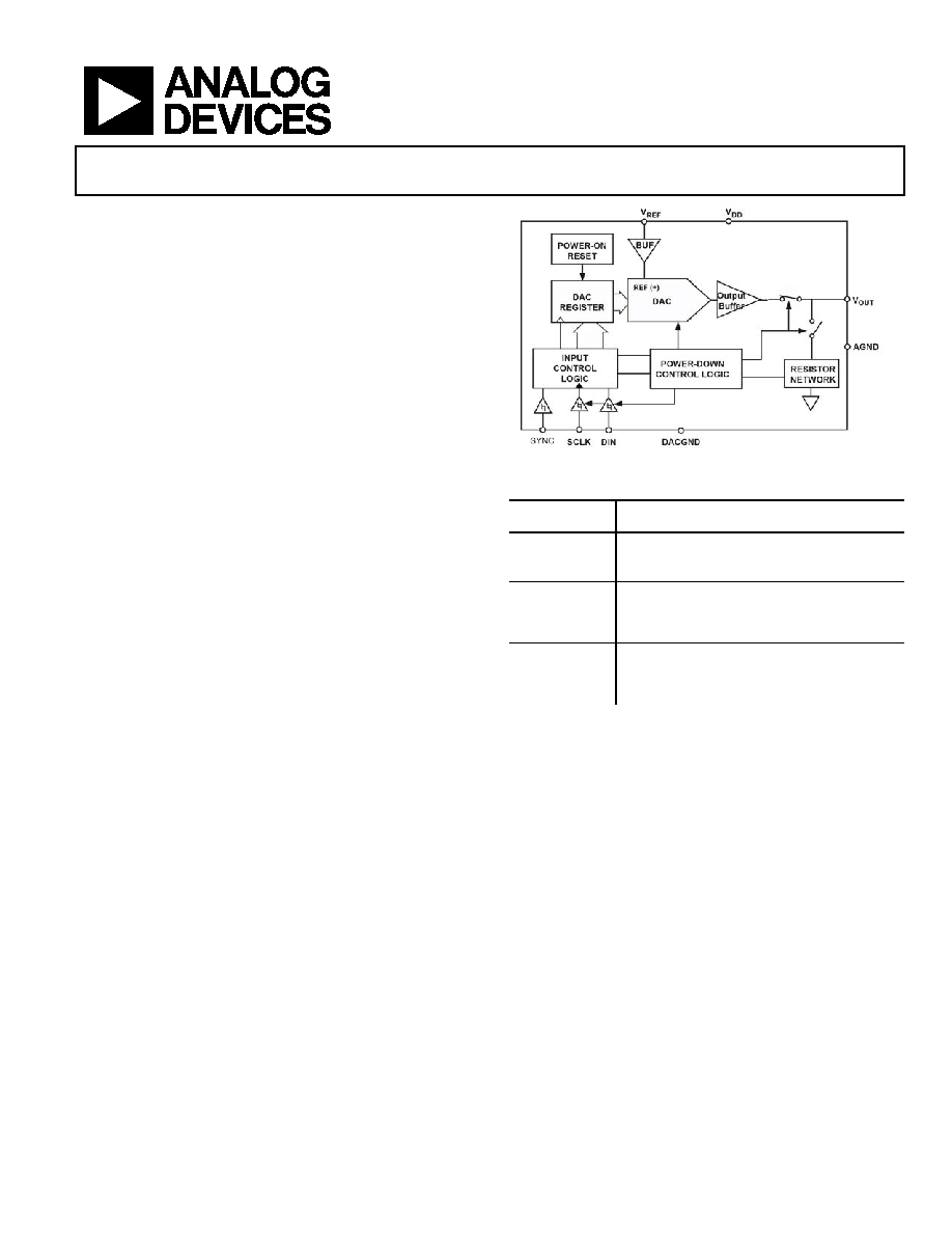
GENERAL DESCRIPTION
The AD5061, a member of the nanoDAC
TM
family, is a single
16-bit buffered voltage out DAC, available in a 8 ld Sot23. The
AD5061 can be operated at 3V/5V.
The part utilizes a versatile three-wire serial interface that
operates at clock rates up to 30 MHz and is compatible with
standard SPITM, QSPITM, MICROWIRETM and DSP interface
standards.
The reference for the AD5061 is supplied from an external
REF pin. A reference buffer is also provided on chip. The parts
incorporate a power-on-reset circuit that ensures that the DAC
output powers up to zero volts/ mid scale and remains there
until a valid write takes place to the device. The parts also
contain a power-down feature that reduces the current
consumption of the device to 50nA at 5 V and provides
software selectable output loads while in power-down mode.
The part is put into power-down mode over the serial interface.
Total unadjusted error for the part is <1mV.
These parts also provide a very low glitch on power-up.
AD5061
Part Number
Description
AD5062
2.7 V to 5.5 V, 16 Bit
nanoDAC
TM
D/A, 1LSBs INL.,
Unbuffered, Sot 23.
AD5063
2.7 V to 5.5 V, 16 Bit
nanoDAC
TM
D/A, 1 LSBs INL.,
Unbuffered, 10 uSOIC, uncommitted bi-polar resistors.
AD5040/60
2.7 V to 5.5 V, 14/16 Bit
nanoDAC
TM
D/A, 1 LSBs
INL, Buffered, Sot23.
PRODUCT HIGHLIGHTS
1. Available in 8-lead SOT23.
2. 16 Bit Accurate, 4 LSB INL.
3. Low Glitch on Power-up.
4. High speed serial interface with clock speeds up to 30 MHz.
5. Three power down modes available to the user.
Rev. PrB
Information furnished by Analog Devices is believed to be accurate and reliable.
However, no responsibility is assumed by Analog Devices for its use, nor for any
infringements of patents or other rights of third parties that may result from its use.
Specifications subject to change without notice. No license is granted by implication
or otherwise under any patent or patent rights of Analog Devices. Trademarks and
registered trademarks are the property of their respective companies.
One Technology Way, P.O. Box 9106, Norwood, MA 02062-9106, U.S.A.
Tel: 781.329.4700
www.analog.com
Fax: 781.326.8703
� 2004 Analog Devices, Inc. All rights reserved.

AD5061
Preliminary Technical Data
Rev. PrB | Page 2 of 17
AD5061--SPECIFICATIONS
1
AD5061, V
DD
= 5.5V, Vref =4.096V, RL=5k, 200pF . T
MIN
to T
MAX
; unless otherwise noted.
Parameter
B Version
1
Min Typ Max
Unit Test
Conditions/Comments
STATIC PERFORMANCE
AD5061
Resolution 16 Bits
Relative Accuracy
�4
LSB
TUE
0.5
mV
Differential Nonlinearity
�1
LSB
Guaranteed Monotonic by Design.
Offset
0.65
uV
Zer Code Error
100
uV
Gain Error
200
uV
Offset Drift
6
�V/�C
Gain Temperature Coefficient
2.5
ppm of FSR/�C
OUTPUT CHARACTERISTICS
Output Voltage Range
0 V
ref
-150mV
V
Output Voltage Settling Time
10
�s
1/4 to 3/4 to +/-1lsb
Slew Rate
1
V/�s
Capacitive Load Stability
470
pF
RL=
1000
pF
RL = 5K
Output Noise Spectral Density
50
nV/
Hz
DAC code=TBD , 1kHz
50
nV/
Hz
DAC code=TBD , 10kHz
Digital-to-Analog Glitch
Impulse
5
nV-s
1 LSB Change Around Major Carry.
Digital Feedthrough
0.5
nV-s
DC Output Impedance
1
REFERENCE
INPUT/OUPUT
Vref Input Range
2 V
DD-100mV
V
Input Current
1
uA
DC Input Impedance
1
M
LOGIC INPUTS
Input Current
�1
�A
V
INL
, Input Low Voltage
0.8
V
V
DD
= +5 V
V
INH
, Input High Voltage
1.8
V
V
DD
= +5 V
V
INL
, Input Low Voltage
0.6
V
V
DD
= +3 V
V
INH
, Input High Voltage
1.4
V
V
DD
= +3 V
Pin Capacitance
3
pF
POWER REQUIREMENTS
V
DD
2.7 3.6
V
AD5060 (3 Volt Option)
I
DD
(Normal
Mode)
DAC Active and Excluding Load Current
V
DD
= +2.7 V to +3.6 V
900
�A
V
IH
= V
DD
and V
IL
= GND
I
DD
(All Power-Down Modes)
V
DD
5.0 5.5
V
AD5060 (5 Volt Option)
I
DD
(Normal
Mode)
DAC Active and Excluding Load Current
V
DD
= +5.0 V to +5.5 V
1.3
mA
V
IH
= V
DD
and V
IL
= GND
I
DD
(All Power-Down Modes)
Preliminary Technical Data
AD5040/AD5060
Rev. PrB | Page 3 of 17
Parameter
B Version
1
Min Typ Max
Unit Test
Conditions/Comments
V
DD
2.7 5.5
V
AD5040
I
DD
(Normal
Mode)
DAC Active and Excluding Load Current
V
DD
= +2.7 V to +5.5 V
I
DD
(All Power-Down Modes)
50
nA
V
IH
= V
DD
and V
IL
= GND
PSSR
0.5
LSB
VDD +/- 10%
NOTES
1Temperature ranges are as follows: B Version: �40�C to +125�C, typical at 25�C.
2Guaranteed by design and characterization, not production tested.
3 Linearity calculated using a reduced code range 480-64716.
Specifications subject to change without notice.
AD5061
Preliminary Technical Data
Rev. PrB | Page 4 of 17
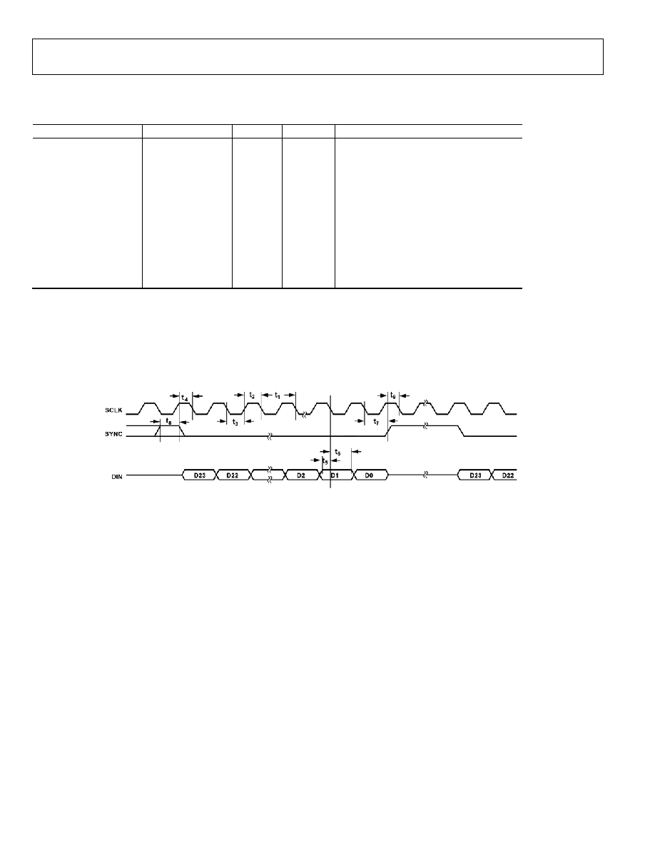
TIMING CHARACTERISTICS
(VDD = 2.7-5.5 V; all specifications TMIN to TMAX unless otherwise noted)
Parameter Limit
1
Unit
Test
Conditions/Comments
t
1
3
33
ns min
SCLK Cycle Time
t
2
13
ns min
SCLK High Time
t
3
12
ns min
SCLK Low Time
t
4
13
ns
min
SYNC to SCLK Falling Edge Setup Time
t
5
5
ns min
Data Setup Time
t
6
4.5
ns min
Data Hold Time
t
7
0
ns min
SCLK Falling Edge to
SYNC Rising Edge
t
8
33
ns min
Minimum
SYNC High Time
t
9
13
ns min
SYNC Rising Edge to next SCLK Fall
Ignore
.
NOTES
1All input signals are specified with tr = tf = 1 ns/V (10% to 90% of VDD) and timed from a voltage level of (VIL + VIH)/2.
2See Figure 1.
3Maximum SCLK frequency is 30 MHz.
Specifications subject to change without notice.
Figure 1. Timing DiagramAD506. AD5040 has same timing specs with 14 bit Word.

Preliminary Technical Data
AD5040/AD5060
Rev. PrB | Page 5 of 17
ABSOLUTE MAXIMUM RATINGS
Table 1. Absolute Maximum Ratings (T
A
= 25�C unless otherwise noted)
Parameter Rating
V
DD
to GND
�0.3 V to + 7.0 V
Digital Input Voltage to GND
�0.3 V to V
DD
+ 0.3 V
V
OUT
to GND
1
�0.3 V to V
DD
+ 0.3 V
Operating Temperature Range
Industrial (B Version)
�40�C to +125�C
Storage Temperature Range
�65�C to +150�C
Maximum Junction Temperature
150�C
SOT23 Package
Power Dissipation
(Tj Max-Ta)/
JA
JA
Thermal Impedance
229.6�C/W
JC
Thermal Impedance
91.99�C/W
Lead Temperature, Soldering
Vapour Phase (60 Sec)
300�C
Infrared (15 Sec)
220�C
Stresses above those listed under Absolute Maximum Ratings may cause permanent damage to the device. This is a stress rating only;
functional operation of the device at these or any other conditions above those listed in the operational sections of this specification is not
implied. Exposure to absolute maximum rating conditions for extended periods may affect device reliability.
This device is a high performance RF integrated circuit with an ESD rating of <2 kV, and it is ESD sensitive. Proper precautions should be
taken for handling and assembly.
Model Temperature
Range
INL Description
Package
Options
AD5061BRJ-1
-40
O
C to 125
O
C
4 LSB
5V, Buffered DAC in SOT-23, Reset to Zero RT8
AD5061BRJ-2
-40
O
C to 125
O
C
4 LSB
5V, Buffered DAC in SOT-23, Reset to Mid
RT8
AD5061BRJ-3
-40
O
C to 125
O
C
4 LSB
3V, Buffered DAC in SOT-23, Reset to Zero
RT8