 | ÐлекÑÑоннÑй компоненÑ: AD5222-50 | СкаÑаÑÑ:  PDF PDF  ZIP ZIP |
AD5222 Data Sheet
REV. 0
Information furnished by Analog Devices is believed to be accurate and
reliable. However, no responsibility is assumed by Analog Devices for its
use, nor for any infringements of patents or other rights of third parties
which may result from its use. No license is granted by implication or
otherwise under any patent or patent rights of Analog Devices.
a
AD5222
One Technology Way, P.O. Box 9106, Norwood, MA 02062-9106, U.S.A.
Tel: 781/329-4700
World Wide Web Site: http://www.analog.com
Fax: 781/326-8703
© Analog Devices, Inc., 1999
Increment/Decrement
Dual Digital Potentiometer
FUNCTIONAL BLOCK DIAGRAM
DECODE
UP/DOWN
COUNTER
AD5222
V
SS
A1
W1
B1
DECODE
UP/DOWN
COUNTER
A2
W2
B2
POR
DAC
SELECT
AND
ENABLE
CLK
CS
U/
D
DACSEL
MODE
GND
V
DD
FEATURES
128-Position, 2-Channel
Potentiometer Replacement
10 k
, 50 k
, 100 k , 1 M
Very Low Power: 40 A Max
2.7 V Dual Supply Operation or
2.7 V to 5.5 V Single Supply Operation
Increment/Decrement Count Control
APPLICATIONS
Stereo Channel Audio Level Control
Mechanical Potentiometer Replacement
Remote Incremental Adjustment Applications
Instrumentation: Gain, Offset Adjustment
Programmable Voltage-to-Current Conversion
Line Impedance Matching
GENERAL DESCRIPTION
The AD5222 provides a dual channel, 128-position, digitally
controlled variable-resistor (VR) device. This device performs
the same electronic adjustment function as a potentiometer or
variable resistor. These products were optimized for instrument
and test equipment push-button applications. Choices between
bandwidth or power dissipation are available as a result of the
wide selection of end-to-end terminal resistance values.
The AD5222 contains two fixed resistors with wiper contacts that
tap the fixed resistor value at a point determined by a digitally
controlled up/down counter. The resistance between the wiper
and either end point of the fixed resistor provides a constant
resistance step size that is equal to the end-to-end resistance
divided by the number of positions (e.g., R
STEP
= 10 k
/128 =
78
). The variable resistor offers a true adjustable value of
resistance, between Terminal A and the wiper, or Terminal B
and the wiper. The fixed A-to-B terminal resistance of 10 k
,
50 k
, 100 k
, or 1 M
has a nominal temperature coefficient
of 35 ppm/
°
C.
The chip select
CS, count CLK and U/D direction control inputs
set the variable resistor position. The MODE determines whether
both VRs are incremented together or independently. With
MODE at logic zero, both wipers are incremented UP or DOWN
without changing the relative settings between the wipers. Also,
the relative ratio between the wipers is preserved if either wiper
reaches the end of the resistor array. In the independent MODE
(Logic 1) only the VR determined by the DACSEL pin is changed.
DACSEL (Logic 0) changes RDAC 1. These inputs, which con-
trol the internal up/down counter, can be easily generated with
mechanical or push-button switches (or other contact closure
devices). This simple digital interface eliminates the need for
microcontrollers in front panel interface designs.
The AD5222 is available in the surface-mount (SO-14) package.
For ultracompact solutions, selected models are available in the
thin TSSOP-14 package. All parts are guaranteed to operate
over the extended industrial temperature range of 40
°
C to
+85
°
C. For 3-wire, SPI-compatible interface applications, see
the AD5203/AD5204/AD5206, AD7376, and AD8400/AD8402/
AD8403 products.
V
SS
A1
W1
B1
A2
W2
B2
CLK
CS
U/
D
DACSEL
MODE
GND
V
DD
U/
D
INCREMENT
5V
Figure 1. Typical Push-Button Control Application

2
REV. 0
AD5222SPECIFICATIONS
(V
DD
= 3 V 10% or 5 V 10%, V
SS
= 0 V, V
A
= +V
DD
, V
B
= 0 V, 40 C < T
A
< +85 C,
unless otherwise noted.)
Parameter
Symbol
Condition
Min
Typ
1
Max
Unit
DC CHARACTERISTICS RHEOSTAT MODE (Specifications Apply to All VRs)
Resistor Differential NL
2
R-DNL
R
WB
, V
A
= NC
1
±
1/4 +1
LSB
Resistor Nonlinearity
2
R-INL
R
WB
, V
A
= NC
1
±
0.4 +1
LSB
Nominal Resistor Tolerance
R
V
AB
= V
DD
, Wiper = No Connect, T
A
= 25
°
C
30
+30
%
Resistance Temperature Coefficient
R
AB
/
T
V
AB
= V
DD
, Wiper = No Connect
35
ppm/
°
C
Wiper Resistance
3
R
W
I
W
= V
DD
/R, V
DD
= 3 V or 5 V
45
100
Nominal Resistance Match
R/R
O
CH 1 to 2, V
AB
= V
DD
, T
A
= 25
°
C
0.2
1
%
DC CHARACTERISTICS POTENTIOMETER DIVIDER MODE (Specifications Apply to All VRs)
Resolution
N
7
Bits
Integral Nonlinearity
4
INL
R
AB
= 10 k
, 50 k
, or 100 k
1
±
1/4 +1
LSB
INL
R
AB
= 1 M
2
±
1/2 +2
LSB
Differential Nonlinearity
4
DNL
1
±
1/4 +1
LSB
Voltage Divider Temperature Coefficient
V
W
/
T
Code = 40
H
20
ppm/
°
C
Full-Scale Error
V
WFSE
Code = 7F
H
1
0.5
+0
LSB
Zero-Scale Error
V
WZSE
Code = 00
H
0
0.5
1
LSB
RESISTOR TERMINALS
Voltage Range
5
V
A, B, W
V
SS
V
DD
V
Capacitance
6
A, B
C
A, B
f = 1 MHz, Measured to GND, Code = 40
H
45
pF
Capacitance
6
W
C
W
f = 1 MHz, Measured to GND, Code = 40
H
60
pF
Common-Mode Leakage
I
CM
V
A
= V
B
= V
W
1
nA
DIGITAL INPUTS AND OUTPUTS
Input Logic High
V
IH
V
DD
= 5 V/3 V
2.4/2.1
V
Input Logic Low
V
IL
V
DD
= 5 V/3 V
0.8/0.6 V
Input Current
I
IL
V
IN
= 0 V or 5 V
±
1
µ
A
Input Capacitance
6
C
IL
5
pF
POWER SUPPLIES
Power Single-Supply Range
V
DD RANGE
V
SS
= 0 V
2.7
5.5
V
Power Dual-Supply Range
V
DD/SS RANGE
±
2.3
±
2.7
V
Positive Supply Current
I
DD
V
IH
= 5 V or V
IL
= 0 V
15
40
µ
A
Negative Supply Current
I
SS
V
SS
= 2.5 V, V
DD
= +2.7 V
15
40
µ
A
Power Dissipation
7
P
DISS
V
IH
= 5 V or V
IL
= 0 V, V
DD
= 5 V
150
400
µ
W
Power Supply Sensitivity
PSS
0.002 0.05
%/%
DYNAMIC CHARACTERISTICS
6, 8, 9
Bandwidth 3 dB
BW_10K
R
AB
= 10 k
, Code = 40
H
1000
kHz
BW_50K
R
AB
= 50 k
, Code = 40
H
180
kHz
BW_100K
R
AB
= 100 k
, Code = 40
H
78
kHz
BW_1M
R
AB
= 500 k
, Code = 40
H
7
kHz
Total Harmonic Distortion
THD
W
V
A
= 1 V rms + 2 V dc, V
B
= 2 V dc, f = 1 kHz
0.005
%
V
W
Settling Time
t
S
R
AB
= 10 k
,
±
1 LSB Error Band
2
µ
s
Resistor Noise Voltage
e
N_WB
R
WB
= 5 k
, f = 1 kHz
14
nV
Hz
INTERFACE TIMING CHARACTERISTICS (Applies to All Parts)
6, 10
Input Clock Pulsewidth
t
CH
, t
CL
Clock Level High or Low
30
ns
CS to CLK Setup Time
t
CSS
20
ns
CS Rise to CLK Hold Time
t
CSH
20
ns
U/
D to Clock Fall Setup Time
t
UDS
10
ns
U/
D to Clock Fall Hold Time
t
UDH
30
ns
DACSEL to Clock Fall Setup Time
t
DSS
20
ns
DACSEL to Clock Fall Hold Time
t
DSH
30
ns
MODE to Clock Fall Setup Time
t
MDS
20
ns
MODE to Clock Fall Hold Time
t
MDH
40
ns
NOTES
1
Typicals represent average readings at 25
°
C, V
DD
= 5 V.
2
Resistor position nonlinearity error R-INL is the deviation from an ideal value measured between the maximum resistance and the minimum resistance wiper positions.
R-DNL measures the relative step change from ideal between successive tap positions. Parts are guaranteed monotonic. See Figure 22 test circuit.
3
Wiper resistance is not measured on the R
AB
= 1 M
models.
4
INL and DNL are measured at V
W
with the RDAC configured as a potentiometer divider similar to a voltage output D/A converter. V
A
= V
DD
and V
B
= 0 V. DNL
specification limits of
±
1 LSB maximum are guaranteed monotonic operating conditions. See Figure 21 test circuit.
5
Resistor Terminals A, B, W have no limitations on polarity with respect to each other.
6
Guaranteed by design and not subject to production test.
7
P
DISS
is calculated from (I
DD
×
V
DD
). CMOS logic level inputs result in minimum power dissipation.
8
Bandwidth, noise and settling time are dependent on the terminal resistance value chosen. The lowest R value results in the fastest settling time and highest bandwidth.
The highest R value results in the minimum overall power consumption.
9
All dynamic characteristics use V
DD
= 5 V.
10
See timing diagram for location of measured values. All input control voltages are specified with t
R
= t
F
= 2.5 ns (10% to 90% of +3 V) and timed from a voltage level
of 1.5 V. Switching characteristics are measured using both V
DD
= 5 V or V
DD
= 3 V.
Specifications subject to change without notice.
AD5222
3
REV. 0
ABSOLUTE MAXIMUM RATINGS
(T
A
= 25
°
C, unless otherwise noted)
V
DD
to GND . . . . . . . . . . . . . . . . . . . . . . . . . . . . 0.3 V, +7 V
V
SS
to GND . . . . . . . . . . . . . . . . . . . . . . . . . . . . . . . 0 V, 5 V
V
DD
to V
SS
. . . . . . . . . . . . . . . . . . . . . . . . . . . . . . . . . . . . . 7 V
V
A
, V
B
, V
W
to GND . . . . . . . . . . . . . . . . . . . . . . . . . . 0 V, V
DD
A
X
B
X
, A
X
W
X
, B
X
W
X
. . . . . . . . . . . . . . . . . . .
±
20 mA
Digital Input Voltage to GND . . . . . . . . . . . . 0 V, V
DD
+ 0.3 V
Operating Temperature Range . . . . . . . . . . . 40
°
C to +85
°
C
Maximum Junction Temperature (T
J
max) . . . . . . . . . . 150
°
C
Storage Temperature . . . . . . . . . . . . . . . . . . 65
°
C to +150
°
C
Lead Temperature (Soldering, 10 sec) . . . . . . . . . . . . . 300
°
C
Package Power Dissipation . . . . . . . . . . . . . (T
J
max T
A
)/
JA
Thermal Resistance
JA
,
SOIC (SO-14) . . . . . . . . . . . . . . . . . . . . . . . . . . . . 158
°
C/W
TSSOP-14 . . . . . . . . . . . . . . . . . . . . . . . . . . . . . . . 206
°
C/W
t
CSS
t
CH
t
CSH
t
UDS
t
CL
CS
CLK
U/
D
t
DSS
DACSEL
t
MDS
MODE
t
UDH
t
DSH
t
MDH
Figure 2. Detail Timing Diagram
Truth Table
CS
CLK
U/
D
Operation
L
t
H
Wiper Increment Toward Terminal A
L
t
L
Wiper Decrement Toward Terminal B
H
X
X
Wiper Position Fixed
Common Mode (MODE = 0) moves both wipers together either
UP or DOWN the resistor array without changing the relative
distance between the wipers. Also, the distance between both
wipers is preserved if either reaches the end of the array. Inde-
pendent Mode (MODE = 1) allows user to control each RDAC
individually: DACSEL = 0 sets RDAC1; DACSEL = 1: sets
RDAC2.
ORDERING GUIDE
Kilo
Package
Package
Model
Ohms Temperature Description Option
AD5222BR10
10
40
°
C/+85
°
C
SO-14
R-14
AD5222BRU10
10
40
°
C/+85
°
C
TSSOP-14
RU-14
AD5222BR50
50
40
°
C/+85
°
C
SO-14
R-14
AD5222BRU50
50
40
°
C/+85
°
C
TSSOP-14
RU-14
AD5222BR100
100
40
°
C/+85
°
C
SO-14
R-14
AD5222BRU100 100
40
°
C/+85
°
C
TSSOP-14
RU-14
AD5222BR1M
1,000
40
°
C/+85
°
C
SO-14
R-14
AD5222BRU1M 1,000
40
°
C/+85
°
C
TSSOP-14
RU-14
The AD5222 die size is 56 mil
×
60 mil, 3360 sq. mil; 1.4224 mm
×
1.524 mm,
2.1677 sq. mm. Contains 1503 transistors. Patent Number 5495245 applies.
CAUTION
ESD (electrostatic discharge) sensitive device. Electrostatic charges as high as 4000 V readily
accumulate on the human body and test equipment and can discharge without detection. Although
the AD5222 features proprietary ESD protection circuitry, permanent damage may occur on
devices subjected to high energy electrostatic discharges. Therefore, proper ESD precautions are
recommended to avoid performance degradation or loss of functionality.
WARNING!
ESD SENSITIVE DEVICE
PIN FUNCTION DESCRIPTIONS
Pin Name
Description
1
B1
B Terminal RDAC #1.
2
A1
A Terminal RDAC #1.
3
W1
Wiper RDAC #1, DACSEL = 0.
4
V
SS
Negative Power Supply. Specified for operation
at both 0 V or 2.7 V (Sum of |V
DD
| + |V
SS
|
< 5.5 V).
5
W2
Wiper RDAC #2, DACSEL = 1.
6
A2
A Terminal RDAC #2.
7
B2
B Terminal RDAC #2.
8
GND
Ground.
9
MODE
Common MODE = 0, Independent MODE = 1.
10
DACSEL DAC Select determines which wiper is incre-
mented in the Independent MODE = 1.
DACSEL = 0 sets RDAC1, DACSEL = 1 sets
RDAC2.
11
U/
D
UP/DOWN Direction Control.
12
CLK
Serial Clock Input, Negative Edge Triggered.
13
CS
Chip Select Input, Active Low. When
CS is
high, the UP/DOWN counter is disabled.
14
V
DD
Positive Power Supply. Specified for operation
at both +3 V or +5 V. (Sum of |V
DD
| + |V
SS
|
< 5.5 V).
PIN CONFIGURATION
TOP VIEW
(Not to Scale)
CLK
U/
D
A1
GND
V
DD
CS
B1
W1
AD5222
1
2
3
4
5
6
7
8
9
10
11
12
13
14
DACSEL
MODE
V
SS
W2
A2
B2
PERCENT OF NOMINAL
END-TO-END RESISTANCE % R
AB
100
75
0
0
32
128
R
WB
64
96
50
25
CODE Decimal
R
WA
Figure 3. Wiper-To-End Terminal Resistance vs. Code
I
WA
CURRENT mA
0
3F
H
R
AB
= 10k
V
DD
= 5V
T
A
= 25 C
2
3
4
5
6
7
0.5
1
1.5
2
2.5
3
3.5
4
4.5
5
0
1
V
WB
VOLTAGE V
08
H
02
H
05
H
10
H
20
H
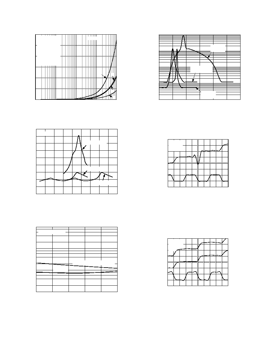
Figure 4. Resistance Linearity vs. Conduction Current
180
90
WIPER RESISTANCE
FREQUENCY
0
40
30
41
42
47 48
50 51
53 54
60
44
45
56 57 59
60
120
150
SS = 600 UNITS
V
DD
= 2.7V
T
A
= 25 C
Figure 5. Wiper Contact Resistance
AD5222Typical Performance Characteristics
4
REV. 0
CODE Decimal
0.25
0.25
0
128
16
R-DNL ERROR LSB
32
48
64
80
96
112
0.20
0.05
0.05
0.15
0.20
0.15
0.10
0
0.10
T
A
= +25 C
T
A
= +85 C
T
A
= 55 C
V
DD
= +15V
V
SS
= 15V
R
AB
= 50k
Figure 6. R-DNL Relative Resistance Step Position
Change vs. Code
CODE Decimal
1.0
1.0
0
128
16
R-INL ERROR LSB
32
48
64
80
96
112
0.8
0.2
0.2
0.6
0.8
0.6
0.4
0
0.4
V
DD
/V
SS
= 2.7V/0V
T
A
= 25 C
50k VERSION
100k VERSION
1M VERSION
10k VERSION
Figure 7. R-INL Resistance Nonlinearity Error vs. Code
CODE Decimal
1.0
0
128
16
INL
LSB
32
48
64
80
96
112
0.2
0.2
0.6
0.8
0.6
0.4
0
0.4
V
DD
/V
SS
= 2.7V/0V
T
A
= 25 C
50k VERSION
100k VERSION
1M VERSION
10k VERSION
Figure 8. Potentiometer Divider INL Error vs. Code
AD5222
5
REV. 0
CODE Decimal
70
30
0
128
16
POTENTIOMETER MODE TEMPCO ppm/
C
32
48
64
80
96
112
50
40
30
60
20
10
0
10
20
V
DD
/V
SS
= 2.7V/0V
T
A
= 25 C
50k VERSION
100k VERSION
1M VERSION
10k VERSION
Figure 9.
V
WB
/ T Potentiometer Mode Tempco
CODE Decimal
120
80
0
128
16
RHEOSTAT MODE TEMPCO ppm/
C
32
48
64
80
96
112
80
60
40
100
20
0
20
40
60
50k
VERSION
10k VERSION
100k VERSION
1M VERSION
V
DD
/V
SS
= 2.7V/0V
T
A
= 25 C
Figure 10.
R
WB
/ T Rheostat Mode Tempco
FREQUENCY Hz
0
50
10
1M
GAIN - dB 30
100
1k
10k
100k
10
20
40
10M
20
H
08
H
10
H
02
H
04
H
01
H
CODE = 3F
H
T
A
= 25 C
SEE TEST CIRCUIT FIGURE 32
Figure 11. 10 k
Gain vs. Frequency vs. Code
FREQUENCY Hz
0
12
1M
GAIN dB
6
100
1k
10k
100k
9
3
9
15
18
21
3
6
V
DD
= +2.7V
V
SS
= 2.7V
DATA = 40
H
V
A
= 50mV rms
V
B
= 0V
10k 764kHz
50k 132kHz
100k 64kHz
1M 6.6kHz
BW
A
B
OP42
W
50k
100k
10k
1M
Figure 12. Gain vs. Frequency vs. R
AB
FREQUENCY Hz
100k
THD + NOISE %
10
100
1k
10k
10
0.001
FILTER = 22kHz
V
DD
= 2.7V
V
IN
= 1V rms
T
A
= 25 C
SEE TEST CIRCUIT FIGURE 26
SEE TEST CIRCUIT FIGURE 25
0.01
0.1
1.0
Figure 13. Total Harmonic Distortion Plus Noise vs.
Frequency
FREQUENCY Hz
10
1M
NORMALIZED GAIN FLATNESS 0.1dB/DIV
100
1k
10k
100k
SEE TEST CIRUIT 27
V
DD
= 2.7V
V
SS
= 2.7V
V
A
= 50mV rms
V
B
= 0V
DATA = 40
H
W
A
B
OP42
10k
50k
100k
1M
Figure 14. Normalized Gain Flatness vs. Frequency
AD5222
6
REV. 0
FREQUENCY Hz
1200
1
10M
I
DD
SUPPLY CURRENT
A
1000
10k
100k
1M
800
600
400
A
B
C
D
200
0
A V
DD
= 5.5V
CODE = 15
H
B V
DD
= 3.3V
CODE = 15
H
C V
DD
= 5.5V
CODE = 3F
H
D V
DD
= 3.3V
CODE = 3F
H
T
A
= 25 C
Figure 15. I
DD
, I
SS
Supply Current vs. Clock Frequency
COMMON MODE Volts
10
3
SWITCH RESISTANCE
100
80
60
40
20
90
70
50
30
T
A
= 25 C
2
1
0
1
2
3
4
5
6
V
DD
/V
SS
= 2.7V
V
DD
/V
SS
= 5.5V/0V
V
DD
/V
SS
= 2.7V/0V
Figure 16. Incremental Wiper Contact Resistance vs.
V
DD
/ V
SS
TEMPERATURE C
1
0.1
0.001
40
85
15
SUPPLY CURRENT mA
0.01
10
35
60
LOGIC = 0V OR V
DD
V
DD
= 2.7V
V
DD
= 5.5V OR V
DD
/V
SS
= 2.7V
Figure 17. Supply Current vs. Temperature
INPUT LOGIC VOLTAGE V
10
1
0.001
0
5
1
SUPPLY CURRENT mA
0.01
2
3
4
6
V
DD
= 5.5V
V
A
= 5.5V
V
DD
/V
SS
= 2.5V
V
A
= 2.5V
V
DD
= 2.7V
V
A
= 2.7V
0.1
Figure 18. Supply Current vs. Input Logic Voltage
20mV/DIV
V
W
CLK
2V/DIV
V
DD
= 2.7V
V
A
= 2.7V
V
B
= 0V
Figure 19. Midscale Transition 3F
H
to 40
H
20mV/DIV
V
DD
= 2.7V
V
A
= 2.7V
V
B
= 0V
V
WA
V
WB
CLK
2V/DIV
Figure 20. Stereo Step Transition, Mode = 0
Parametric Test CircuitsAD5222
7
REV. 0
V+
DUT
V
MS
A
B
W
V+ = V
DD
1LSB = V+/128
Figure 21. Potentiometer Divider Nonlinearity Error Test
Circuit (INL, DNL)
NO CONNECT
I
W
DUT
V
MS
A
B
W
Figure 22. Resistor Position Nonlinearity Error (Rheostat
Operation; R-INL, R-DNL)
V
MS2
V
W
I
W
=
V
DD
/R
NOMINAL
DUT
V
MS1
A
B
W
R
W
= [V
MS1
V
MS2
]/I
W
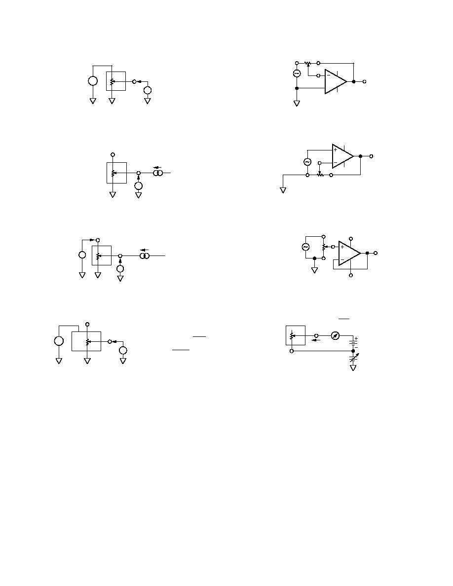
Figure 23. Wiper Resistance Test Circuit
PSRR (dB) = 20 LOG
(
)
PSS (%/%) =
V
MS
V
DD
V
MS
%
V
DD
%
V+ = V
DD
± 10%
V
DD
V
A
~
V+
V
MS
A
B
W
Figure 24. Power Supply Sensitivity Test Circuit (PSS,
PSRR)
A
B
V
IN
OP279
+5V
V
OUT
DUT
W
+
5V
Figure 25. Inverting Programmable Gain Test Circuit
+5V
5V
A
B
V
IN
V
OUT
DUT
W
OP279
Figure 26. Noninverting Programmable Gain Test Circuit
A
B
DUT
W
V
IN
OP42
+15V
V
OUT
15V
Figure 27. Gain vs. Frequency Test Circuit
I
SW
0 TO V
DD
R
SW
=
0.1V
I
SW
CODE = 00
H
0.1V
DUT
B
W
Figure 28. Incremental ON Resistance Test Circuit
AD5222
8
REV. 0
OPERATION
The AD5222 provides a 128-position, digitally-controlled, variable
resistor (VR) device. Changing the VR settings is accomplished
by pulsing the CLK pin while
CS is active low. The U/D (UP/
DOWN) control input pin controls the direction of the increment.
When the wiper hits the end of the resistor (Terminal A or B)
additional CLK pulses no longer change the wiper setting. The
wiper position is immediately decoded by the wiper decode logic
changing the wiper resistance. Appropriate debounce circuitry is
required when push-button switches are used to control the
count sequence and direction of count. The exact timing require-
ments are shown in Figure 2. The AD5222 powers ON in a
centered wiper position, exhibiting nearly equal resistances of
R
WA
and R
WB
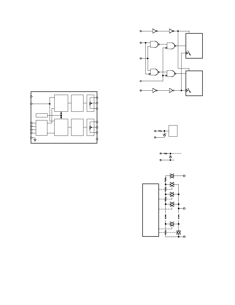
.
DECODE
UP/DOWN
COUNTER
AD5222
V
SS
A1
W1
B1
DECODE
UP/DOWN
COUNTER
A2
W2
B2
POR
DAC
SELECT
AND
ENABLE
CLK
CS
U/
D
DACSEL
MODE
GND
V
DD
Figure 29. Block Diagram
DIGITAL INTERFACING OPERATION
The AD5222 contains a push-button controllable interface. The
active inputs are clock (CLK),
CS and up/down (U/D). While
the MODE, and DACSEL pins control common updates or
individual updates. The negative-edge sensitive CLK input
requires clean transitions to avoid clocking multiple pulses into
the internal UP/DOWN counter register, Figure 30. Standard
logic families work well. If mechanical switches are used for
product evaluation a flip-flop or other suitable means should
debounce them. When
CS is taken active low, the clock begins
to increment or decrement the internal up/down counter, depen-
dent upon the state of the U/
D control pin. The UP/DOWN
counter value (D) starts at 40
H
at system power ON. Each new
CLK pulse will increment the value of the internal counter by
1 LSB until the full-scale value of 7F
H
is reached, as long as the
U/
D pin is logic high. If the U/D pin is taken to logic low, the
counter will count down, stopping at code 00
H
(zero-scale).
Additional clock pulses on the CLK pin are ignored when the
wiper is at either the 00
H
position or the 7F
H
position. The
detailed digital logic interface circuitry is shown in Figure 30.
RDAC 1
U/
D
COUNTER
RDAC 2
U/
D
COUNTER
CLK
CS
U/
D
DACSEL
MODE
Figure 30. Detailed Digital Logic Interface Circuit
All digital inputs (
CS, U/D, CLK, MODE, DACSEL) are
protected with a series input resistor and parallel Zener ESD
structure shown in Figure 31. All potentiometer terminal pins
(A, B, W) are protected from ESD as shown in Figure 32.
LOGIC
1k
V
SS
Figure 31. Equivalent ESD Protection Digital Pins
20
A, B, W
V
SS
Figure 32. Equivalent ESD Protection Analog Pins
D0
D1
D2
D3
D4
D5
D6
RDAC
UP/DOWN
CNTR
&
DECODE
W
B
R
S
= R
NOMINAL
/128
R
S
R
S
R
S
A
R
S
Figure 33. AD5222 Equivalent RDAC Circuit

AD5222
9
REV. 0
PROGRAMMING THE VARIABLE RESISTOR
Rheostat Operation
The nominal resistance of the RDAC between Terminals A and
B are available with values of 10 k
, 50 k
, 100 k
, and 1 M
The final three characters of the part number determine the
nominal resistance value, e.g., 10 k
= 10; 50 k
= 50; 100 k
= 100; 1 M
= 1M. The nominal resistance (R
AB
) of the VR
has 128 contact points accessed by the wiper terminal, plus the
B terminal contact. At power ON, the resistance from the wiper
to either end Terminal A or B is approximately equal. Pulsing
the CLK pin will increase the resistance from the wiper W to
Terminal B by one unit of R
S
resistance, see Figure 33. The
resistance R
WB
is determined by the number of pulses applied to
the clock pin. Each segment of the internal resistor string has a
nominal resistance value of R
S
= R
AB
/128, which becomes 78
in the case of the 10 k
AD5222BR10 product. Care should be
taken to limit the current flow between W and B in the direct
contact state (R
WB
code = 0) to a maximum value of 20 mA to
avoid degradation or possible destruction of the internal switch
contact.
Like the mechanical potentiometer the RDAC replaces, it is
totally symmetrical (see Figure 3). The resistance between the
wiper W and Terminal A also produces a digitally controlled
resistance R
WA
. When these terminals are used the B-terminal
should be tied to the wiper.
The typical part-to-part distribution of R
BA
is process-lot-
dependent having a
±
30% variation. The change in R
BA
with
temperature has a 35 ppm/
°
C temperature coefficient.
The R
BA
temperature coefficient increases as the wiper is pro-
grammed near the B-terminal due to the larger percentage
contribution of the wiper contact switch resistance, which has a
0.5%/
°
C temperature coefficient. Figures 9 and 10 show the
effect of the wiper contact resistance as a function of code setting.
PROGRAMMING THE POTENTIOMETER DIVIDER
Voltage Output Operation
The digital potentiometer easily generates an output voltage
proportional to the input voltage applied to a given terminal.
For example connecting A-terminal to 5 V and B-terminal to
ground produces an output voltage at the wiper which can be
any value starting at zero volts up to 1 LSB less than 5 V. Each
LSB of voltage is equal to the voltage applied across Terminals
AB divided by the 128-position resolution of the potentiometer
divider. The general equation defining the output voltage with
respect to ground for any given input voltage applied to Termi-
nals AB is:
V
W
(D) = D/128
×
V
AB
+ V
B
(1)
D represents the current contents of the internal up/down counter.
Operation of the digital potentiometer in the divider mode
results in more accurate operation over temperature. Here the
output voltage is dependent on the ratio of the internal resistors
not the absolute value, therefore, the drift improves to 20 ppm/
°
C.
AD5222
10
REV. 0
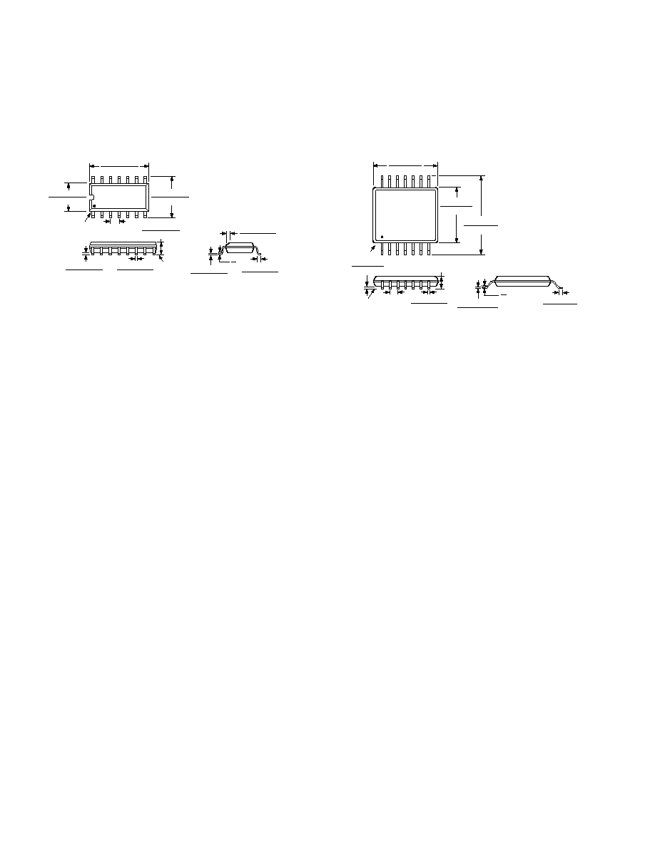
OUTLINE DIMENSIONS
Dimensions shown in inches and (mm).
14-Lead Narrow Body SOIC
(R-14)
14
8
7
1
0.2440 (6.20)
0.2284 (5.80)
0.1574 (4.00)
0.1497 (3.80)
PIN 1
0.3444 (8.75)
0.3367 (8.55)
0.050 (1.27)
BSC
SEATING
PLANE
0.0098 (0.25)
0.0040 (0.10)
0.0192 (0.49)
0.0138 (0.35)
0.0688 (1.75)
0.0532 (1.35)
8
0
0.0196 (0.50)
0.0099 (0.25)
45
0.0500 (1.27)
0.0160 (0.41)
0.0099 (0.25)
0.0075 (0.19)
14-Lead TSSOP
(RU-14)
14
8
7
1
0.256 (6.50)
0.246 (6.25)
0.177 (4.50)
0.169 (4.30)
PIN 1
0.201 (5.10)
0.193 (4.90)
SEATING
PLANE
0.006 (0.15)
0.002 (0.05)
0.0118 (0.30)
0.0075 (0.19)
0.0256
(0.65)
BSC
0.0433 (1.10)
MAX
0.0079 (0.20)
0.0035 (0.090)
0.028 (0.70)
0.020 (0.50)
8
0
C3715810/99
PRINTED IN U.S.A.