Document Outline
- FEATURES
- APPLICATIONS
- FUNCTIONAL BLOCK DIAGRAM
- GENERAL DESCRIPTION
- ˛ˇ
- ˛ˇ
- ˛ˇ
- ˛ˇ
- ˛ˇ
- ˛ˇ
- ˛ˇ

64-Position Up/Down
Control Digital Potentiometer
AD5227
Rev. 0
Information furnished by Analog Devices is believed to be accurate and reliable.
However, no responsibility is assumed by Analog Devices for its use, nor for any
infringements of patents or other rights of third parties that may result from its use.
Specifications subject to change without notice. No license is granted by implication
or otherwise under any patent or patent rights of Analog Devices. Trademarks and
registered trademarks are the property of their respective owners.
One Technology Way, P.O. Box 9106, Norwood, MA 02062-9106, U.S.A.
Tel: 781.329.4700
www.analog.com
Fax: 781.326.8703
© 2004 Analog Devices, Inc. All rights reserved.
FEATURES
64-position digital potentiometer
10 k, 50 k, 100 k end-to-end terminal resistance
Simple up/down digital or manual configurable control
Midscale preset
Low potentiometer mode tempco = 10 ppm/∞C
Low rheostat mode tempco = 35 ppm/∞C
Ultralow power, I
DD
= 0.4 µA typ and 3 µA max
Fast adjustment time, ts = 1 µs
Chip select enable multiple device operation
Low operating voltage, 2.7 V to 5.5 V
Automotive temperature range, -40∞C to +105∞C
Compact thin SOT-23-8 (2.9 mm ◊ 3 mm) Pb-free package
APPLICATIONS
Mechanical potentiometer and trimmer replacements
LCD backlight, contrast, and brightness controls
Portable electronics level adjustment
Programmable power supply
Digital trimmer replacements
Automatic closed-loop control
FUNCTIONAL BLOCK DIAGRAM
04419-0-001
CS
U/D
CLK
GND
V
DD
6-BIT UP/DOWN
CONTROL
LOGIC
POR
MIDSCALE
WIPER
REGISTER
A
W
B
AD5227
Figure 1.
GENERAL DESCRIPTION
The AD5227 is Analog Devices' latest 64-step up/down control
digital potentiometer
1
. This device performs the same electronic
adjustment function as a 5 V potentiometer or variable resistor.
Its simple 3-wire up/down interface allows manual switching or
high speed digital control. The AD5227 presets to midscale at
power-up. When CS is enabled, the devices changes step at
every clock pulse. The direction is determined by the state of
the U/D pin (see Table 1). The interface is simple to activate by
any host controller, discrete logic, or manually with a rotary
encoder or pushbuttons. The AD5227's 64-step resolution, small
footprint, and simple interface enable it to replace mechanical
potentiometers and trimmers with typically 6◊ improved
resolution, solid-state reliability, and design layout flexibility,
resulting in a considerable cost savings in end users' systems.
1
The terms digital potentiometer and RDAC are used interchangeably.
The AD5227 is available in a compact thin SOT-23-8 (TSOT-8)
Pb-free package. The part is guaranteed to operate over the
automotive temperature range of -40∞C to +105∞C.
Users who consider EEMEM potentiometers should refer to
some recommendations in the Applications section.
Table 1. Truth Table
CS
CLK
U/D
Operation
1
0
0
R
WB
Decrement
0
1
R
WB
Increment
1
X
X
No Operation
1
R
WA
increments if R
WB
decrements and vice versa.

AD5227
Rev. 0 | Page 2 of 16
TABLE OF CONTENTS
Electrical Characteristics ................................................................. 3
Interface Timing Diagrams ......................................................... 4
Absolute Maximum Ratings............................................................ 5
ESD Caution.................................................................................. 5
Pin Configuration and Function Descriptions............................. 6
Typical Performance Characteristics ............................................. 7
Theory of Operation ...................................................................... 10
Programming the Digital Potentiometers............................... 10
Digital Interface .......................................................................... 11
Terminal Voltage Operation Range.......................................... 11
Power-Up and Power-Down Sequences.................................. 11
Layout and Power Supply Biasing ............................................ 11
Applications..................................................................................... 12
Manual Control with Toggle and Pushbutton Switches........ 12
Manual Control with Rotary Encoder..................................... 12
Adjustable LED Driver .............................................................. 12
Adjustable Current Source for LED Driver ............................ 12
Automatic LCD Panel Backlight Control................................ 13
6-Bit Controller .......................................................................... 13
Constant Bias with Supply to Retain Resistance Setting...... 14
Outline Dimensions ....................................................................... 15
Ordering Guide .......................................................................... 15
REVISION HISTORY
Revision 0: Initial Version

AD5227
Rev. 0 | Page 3 of 16
ELECTRICAL CHARACTERISTICS
10 k, 50 k, 100 k versions: V
DD
= 3 V ± 10% or 5 V ± 10%, V
A
= V
DD
, V
B
= 0 V, -40∞C < T
A
< +105∞C, unless otherwise noted.
Table 2.
Parameter
Symbol
Conditions
Min
Typ
1
Max
Unit
DC CHARACTERISTICS RHEOSTAT MODE
Resistor Differential Nonlinearity
2
R-DNL
R
WB
, A = no connect
-0.5 ±0.15
+0.5
LSB
Resistor Integral Nonlinearity
2
R-INL
R
WB
, A = no connect
-1
±0.3
+1
LSB
Nominal Resistor Tolerance
3
R
AB
/R
AB
-20
+20
%
Resistance Temperature Coefficient
(R
AB
/R
AB
)/T ◊ 10
6
35
ppm/∞C
Wiper Resistance
R
W
V
DD
= 2.7 V
100
200
V
DD
= 5.5 V
50
DC CHARACTERISTICS POTENTIOMETER DIVIDER MODE
Resolution
N
6
Bits
Integral Nonlinearity
3
INL
-1
±0.1
+1
LSB
Differential Nonlinearity
3, 4
DNL
-0.5 ±0.1
+0.5
LSB
Voltage Divider Temperature Coefficient
(V
W
/V
W
)/T ◊ 10
6
Midscale
5
ppm/∞C
Full-Scale Error
V
WFSE
+31 steps from midscale
-1
-0.5
0
LSB
Zero-Scale Error
V
WZSE
-32 steps from midscale
0
0.5
+1
LSB
RESISTOR TERMINALS
Voltage Range
5
V
A, B, W
With respect to GND
0
V
DD
V
Capacitance A, B
6
C
A, B
f = 1 MHz, measured to
GND
140
pF
Capacitance W
6
C
W
f = 1 MHz, measured to
GND
150
pF
Common-Mode Leakage
I
CM
V
A
= V
B
= V
W
1
nA
DIGITAL INPUTS (CS, CLK, U/D)
Input Logic High
V
IH
2.4
5.5
V
Input Logic Low
V
IL
0
0.8
V
Input Current
I
I
V
IN
= 0 V or 5 V
±1
µA
Input Capacitance
6
C
I
5
pF
POWER SUPPLIES
Power Supply Range
V
DD
2.7
5.5
V
Supply Current
I
DD
V
IH
= 5 V or V
IL
= 0 V,
V
DD
= 5 V
0.4
3
µA
Power Dissipation
7
P
DISS
V
IH
= 5 V or V
IL
= 0 V,
V
DD
= 5 V
17
µW
Power Supply Sensitivity
PSSR
V
DD
= 5 V ± 10%
0.01
0.05
%/%
DYNAMIC CHARACTERISTICS
6,
8,
9
Bandwidth ≠3 dB
BW_10 k
R
AB
= 10 k, midscale
460
kHz
BW_50 k
R
AB
= 50 k, midscale
100
kHz
BW_100 k
R
AB
= 100 k, midscale
50
kHz
Total Harmonic Distortion
THD
V
A
= 1 V rms, R
AB
= 10 k,
V
B
= 0 V dc, f = 1 kHz
0.05
%
Adjustment Settling Time
t
S
V
A
= 5 V ± 1 LSB error
band, V
B
= 0, measured at
V
W
1
µs
Resistor Noise Voltage
e
N_WB
R
WB
= 5 k, f = 1 kHz
14
nV/Hz
Footnotes on the next page.
AD5227
Rev. 0 | Page 4 of 16
Parameter
Symbol
Conditions
Min
Typ
1
Max
Unit
INTERFACE TIMING CHARACTERISTICS (applies to all parts
6, 10
)
Clock Frequency
f
CLK
50
MHz
Input Clock Pulse Width
t
CH
, t
CL
Clock level high or low
10
ns
CS to CLK Setup Time
t
CSS
10
ns
CS Rise to CLK Hold Time
t
CSH
10
ns
U/D to Clock Fall Setup Time
t
UDS
10
ns
1
Typicals represent average readings at 25∞C, V
DD
= 5 V.
2
Resistor position nonlinearity error, R-INL, is the deviation from an ideal value measured between the maximum resistance and the minimum resistance wiper
positions. R-DNL measures the relative step change from ideal between successive tap positions. Parts are guaranteed monotonic.
3
NL and DNL are measured at V
W
with the RDAC configured as a potentiometer divider similar to a voltage output D/A converter. V
A
= V
DD
and V
B
= 0 V.
4
DNL specification limits of ±1 LSB maximum are guaranteed monotonic operating conditions.
5
Resistor Terminals A, B, W have no limitations on polarity with respect to each other.
6
Guaranteed by design and not subject to production test.
7
P
DISS
is calculated from (I
DD
◊ V
DD
). CMOS logic level inputs result in minimum power dissipation.
8
Bandwidth, noise, and settling time are dependent on the terminal resistance value chosen. The lowest R value results in the fastest settling time and highest
bandwidth. The highest R value results in the minimum overall power consumption.
9
All dynamic characteristics use V
DD
= V.
10
All input control voltages are specified with t
R
= t
F
= 1 ns (10% to 90% of V
DD
) and timed from a voltage level of 1.6 V. Switching characteristics are measured using
V
DD
= 5 V.
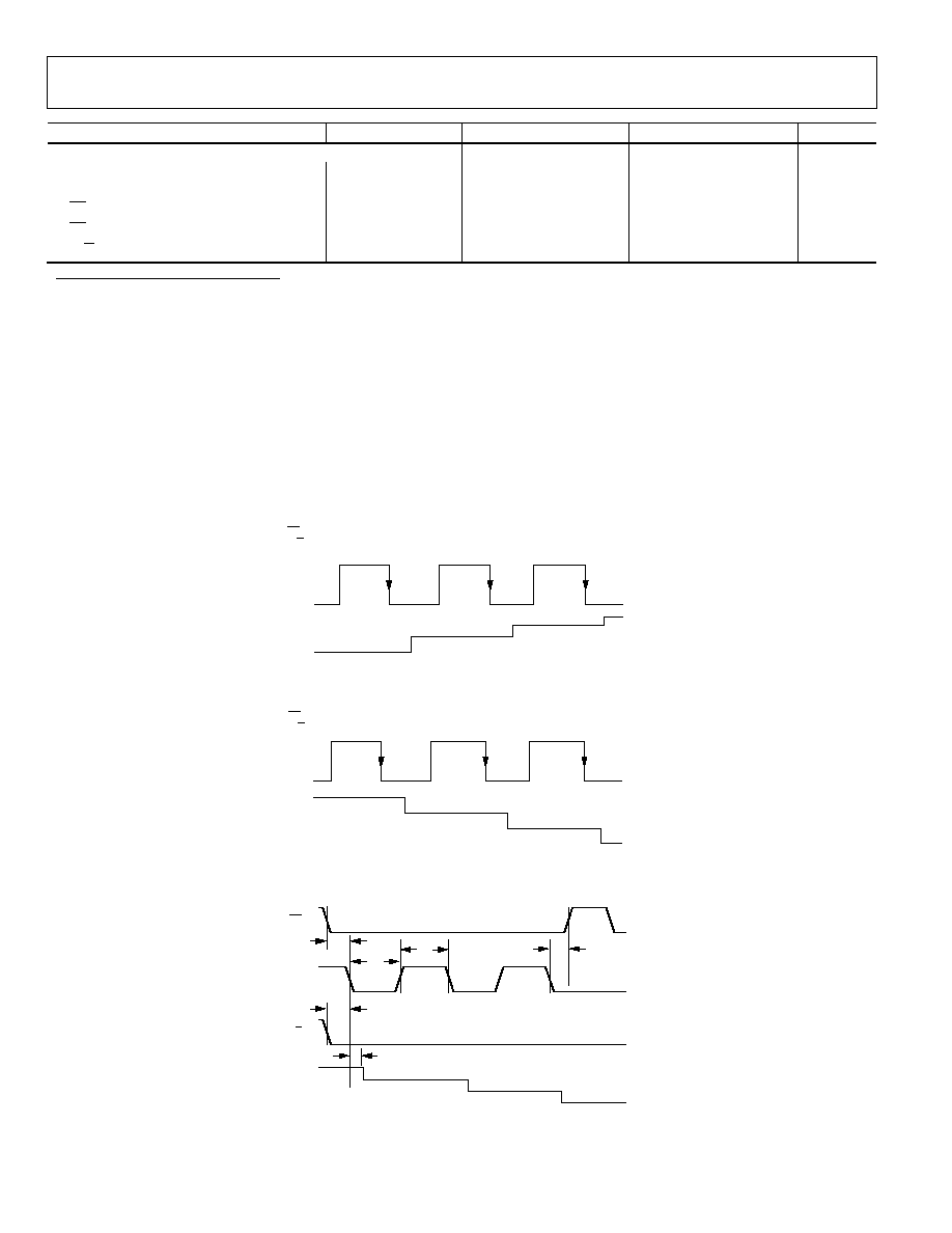
INTERFACE TIMING DIAGRAMS
04419-0-004
CS = LOW
U/D = HIGH
CLK
R
WB
Figure 2. Increment R
WB
04419-0-005
CS = LOW
U/D = 0
CLK
R
WB
Figure 3. Decrement R
WB
04419-0-006
1
0
1
0
1
0
CS
CLK
U/D
R
WB
t
S
t
UDS
t
CL
t
CH
t
CSS
t
CSH
Figure 4. Detailed Timing Diagram(Only R
WB
Decrement Shown)

AD5227
Rev. 0 | Page 5 of 16
ABSOLUTE MAXIMUM RATINGS
Table 3.
Parameter
Rating
V
DD
to GND
-0.3 V, +7 V
V
A
, V
B
, V
W
to GND
0 V, V
DD
Digital Input Voltage to GND (CS, CLK, U/D)
0 V, V
DD
Maximum Current
I
WB
, I
WA
Pulsed
±20 mA
I
WB
Continuous (R
WB
5 k, A open)
1
±1 mA
I
WA
Continuous (R
WA
5 k, B open)
1
±1
mA
I
AB
Continuous
(R
AB
= 10 k/50 k/100 k)
1
±500 µA/
±100 µA/±50 µA
Operating Temperature Range
-40∞C to +105∞C
Maximum Junction Temperature (T
J
max)
150∞C
Storage Temperature
-65∞C to +150∞C
Lead Temperature (Soldering, 10 s ≠ 30 s)
245∞C
Thermal Resistance
2
JA
230∞C/W
1
Maximum terminal current is bounded by the maximum applied voltage
across any two of the A, B, and W terminals at a given resistance, the
maximum current handling of the switches, and the maximum power
dissipation of the package. V
DD
= 5 V.
2
Package power dissipation = (T
J
max ≠ T
A
) /
JA
.
Stresses above those listed under Absolute Maximum Ratings
may cause permanent damage to the device. This is a stress
rating only and functional operation of the device at these or
any other conditions above those indicated in the operational
section of this specification is not implied. Exposure to absolute
maximum rating conditions for extended periods may affect
device reliability.
ESD CAUTION
ESD (electrostatic discharge) sensitive device. Electrostatic charges as high as 4000 V readily accumulate on
the human body and test equipment and can discharge without detection. Although this product features
proprietary ESD protection circuitry, permanent damage may occur on devices subjected to high energy
electrostatic discharges. Therefore, proper ESD precautions are recommended to avoid performance
degradation or loss of functionality.