Äîêóìåíòàöèÿ è îïèñàíèÿ www.docs.chipfind.ru
128-Position I
2
C Compatible
Digital Resistor
AD5246
FEATURES
128-position
End-to-end resistance 5 k, 10 k, 50 k, 100 k
Ultracompact SC70-6 (2 mm × 2.1 mm) package
I
2
C® compatible interface
Full read/write of wiper register
Power-on preset to midscale
Single supply 2.7 V to 5.5 V
Low temperature coefficient 45 ppm/°C
Low power, I
DD
= 3 µA typical
Wide operating temperature 40°C to +125°C
Evaluation board available
APPLICATIONS
Mechanical potentiometer replacement in new designs
Rev. 0
Transducer adjustment of pressure, temperature, position,
chemical, and optical sensors
RF amplifier biasing
Automotive electronics adjustment
Gain control and offset adjustment
GENERAL OVERVIEW
The AD5246 provides a compact 2 mm × 2.1 mm packaged
solution for 128-position adjustment applications. This device
performs the same electronic adjustment function as a variable
resistor. Available in four different end-to-end resistance values
(5 k, 10 k, 50 k, 100 k), these low temperature coefficient
devices are ideal for high accuracy and stability variable
resistance adjustments.
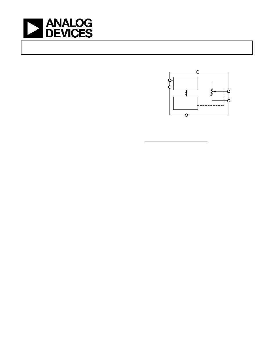
The wiper settings are controllable through the I
2
C compatible
digital interface, which can also be used to read back the present
wiper register control word. The resistance between the wiper
and either end point of the fixed resistor varies linearly with
respect to the digital code transferred into the RDAC
1
latch.
Operating from a 2.7 V to 5.5 V power supply and consuming
3 µA allows for usage in portable battery-operated applications.
FUNCTIONAL BLOCK DIAGRAM
I
2
C INTERFACE
WIPER
REGISTER
SDA
SCL
GND
V
DD
A
W
03875-0-001
B
Figure 1.
1
Note: The terms digital potentiometer, VR, and RDAC are used
interchangeably in this document.
Information furnished by Analog Devices is believed to be accurate and reliable.
However, no responsibility is assumed by Analog Devices for its use, nor for any
infringements of patents or other rights of third parties that may result from its use.
Specifications subject to change without notice. No license is granted by implication
or otherwise under any patent or patent rights of Analog Devices. Trademarks and
registered trademarks are the property of their respective companies.
One Technology Way, P.O. Box 9106, Norwood, MA 02062-9106, U.S.A.
Tel: 781.329.4700
www.analog.com
Fax: 781.326.8703
© 2003 Analog Devices, Inc. All rights reserved.

AD5246
TABLE OF CONTENTS
Electrical Characteristics--5 k Version ...................................... 3
Electrical Characteristics--10 k, 50 k, 100 k Versions ....... 4
Timing Characteristics--5 k, 10 k, 50 k, 100 k Versions 5
Absolute Maximum Ratings............................................................ 6
Typical Performance Characteristics ............................................. 7
Test Circuits..................................................................................... 10
I
2
C Interface..................................................................................... 11
Operation......................................................................................... 12
Programming the Variable Resistor ......................................... 12
I
2
C Compatible 2-Wire Serial Bus............................................ 13
Level Shifting for Bidirectional Interface ................................ 13
ESD Protection ........................................................................... 13
Terminal Voltage Operating Range.......................................... 14
Maximum Operating Current .................................................. 14
Power-Up Sequence ................................................................... 14
Layout and Power Supply Bypassing ....................................... 14
Constant Bias to Retain Resistance Setting............................. 15
Evaluation Board ........................................................................ 15
Pin Configuration and Function Descriptions........................... 16
Outline Dimensions ....................................................................... 17
Ordering Guide .......................................................................... 17
REVISION HISTORY
Revision 0: Initial Version
Rev. 0 | Page 2 of 20

AD5246
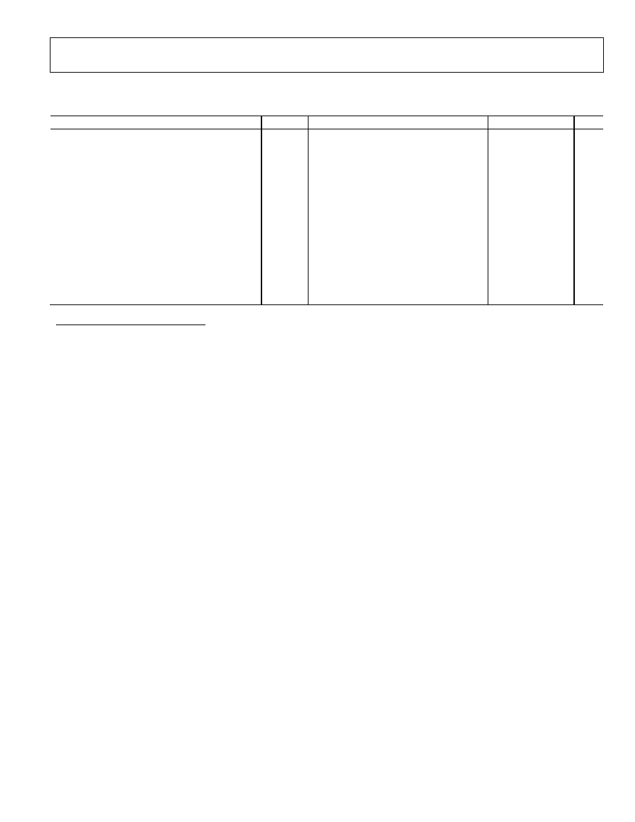
ELECTRICAL CHARACTERISTICS--5 k VERSION
Table 1. V
DD
= 5 V ±10% or 3 V ± 10%; V
A
= +V
DD
; 40°C < T
A
< +125°C; unless otherwise noted
Parameter Symbol
Conditions Min
Typ
1
Max Unit
DC CHARACTERISTICS--RHEOSTAT MODE
Resistor Differential Nonlinearity
2
R-DNL
R
WB
1.5
±0.1
+1.5
LSB
Resistor Integral Nonlinearity
2
R-INL
R
WB
4
±0.75
+4
LSB
Nominal Resistor Tolerance
3
R
AB
T
A
= 25°C
30
+30
%
Resistance Temperature Coefficient
R
AB
/T
Wiper = No Connect
45
ppm/°C
R
WB
R
WB
Code=0x00,
V
DD
= 5 V
75
150
Code=0x00,
V
DD
= 2.7 V
150
400
RESISTOR TERMINALS
Voltage Range
4
V
B, W
GND
V
DD
V
Capacitance
5
B
C
B
f = 1 MHz, Measured to GND, Code = 0x40
45
pF
Capacitance
5
W
C
W
f = 1 MHz, Measured to GND, Code = 0x40
60
pF
Common-Mode Leakage
I
CM
1
nA
DIGITAL INPUTS AND OUTPUTS
Input Logic High
V
IH
V
DD
= 5 V
2.4
V
Input Logic Low
V
IL
V
DD
= 5 V
0.8
V
Input Logic High
V
IH
V
DD
= 3 V
2.1
V
Input Logic Low
V
IL
V
DD
= 3 V
0.6
V
Input Current
I
IL
V
IN
= 0 V or 5 V
±1
µA
Input Capacitance
5
C
IL
5
pF
POWER SUPPLIES
Power Supply Range
V
DD RANGE
2.7
5.5
V
Supply Current
I
DD
V
IH
= 5 V or V
IL
= 0 V
3
8
µA
Power Dissipation
6
P
DISS
V
IH
= 5 V or V
IL
= 0 V, V
DD
= 5 V
40
µW
Power Supply Sensitivity
PSSR
V
DD
= +5 V ± 10%, Code = Midscale
±0.01
±0.02
%/%
DYNAMIC CHARACTERISTICS
5, 7
Bandwidth 3 dB
BW_5K
R
AB
= 5 k, Code = 0x40
1.2
MHz
Total Harmonic Distortion
THD
W
V
A
= 1 V rms, V
B
= 0 V, f = 1 kHz
0.05
%
V
W
Settling Time
t
S
V
A
= 5 V, ±1 LSB Error Band
1
µs
Resistor Noise Voltage Density
e
N_WB
R
WB
= 2.5 k, R
S
= 0
6
nV/Hz
1
Typical specifications represent average readings at 25°C and V
DD
= 5 V.
2
Resistor position nonlinearity error R-INL is the deviation from an ideal value measured between the maximum resistance and the minimum resistance wiper
positions. R-DNL measures the relative step change from ideal between successive tap positions. Parts are guaranteed monotonic.
3
Code = 0x7F.
4
Resistor terminals A and W have no limitations on polarity with respect to each other.
5
Guaranteed by design and not subject to production test.
6
P
DISS
is calculated from (I
DD
× V
DD
). CMOS logic level inputs result in minimum power dissipation.
7
All dynamic characteristics use V
DD
= 5 V.
Rev. 0 | Page 3 of 20

AD5246
ELECTRICAL CHARACTERISTICS--10 k, 50 k, 100 k VERSIONS
Table 2. V
DD
= 5 V ± 10% or 3 V ± 10%; V
A
= V
DD
; 40°C < T
A
< +125°C; unless otherwise noted
Parameter Symbol
Conditions Min
Typ
1
Max
Unit
DC CHARACTERISTICS--RHEOSTAT MODE
Resistor Differential Nonlinearity
2
R-DNL
R
WB
, V
A
= No Connect
1
±0.1
+1
LSB
Resistor Integral Nonlinearity
2
R-INL
R
WB
, V
A
= No Connect
2
±0.25
+2
LSB
Nominal Resistor Tolerance
3
R
AB
T
A
= 25°C
20
+20
%
Resistance Temperature Coefficient
R
AB
/T
Wiper = No Connect
45
ppm/°C
R
WB
R
WB
Code=0x00,
V
DD
= 5 V
75
150
Code=0x00,
V
DD
= 2.7 V
150
400
RESISTOR TERMINALS
Voltage Range
4
V
B, W
GND
V
DD
V
Capacitance
5
B
C
B
f = 1 MHz, Measured to GND, Code = 0x40
45
pF
Capacitance
5
W
C
W
f = 1 MHz, measured to GND, Code = 0x40
60
pF
Common-Mode Leakage
I
CM
1
nA
DIGITAL INPUTS AND OUTPUTS
Input Logic High
V
IH
V
DD
= 5 V
2.4
V
Input Logic Low
V
IL
V
DD
= 5 V
0.8
V
Input Logic High
V
IH
V
DD
= 3 V
2.1
V
Input Logic Low
V
IL
V
DD
= 3 V
0.6
V
Input Current
I
IL
V
IN
= 0 V or 5 V
±1
µA
Input Capacitance
5
C
IL
5
pF
POWER SUPPLIES
Power Supply Range
V
DD RANGE
2.7
5.5
V
Supply Current
I
DD
V
IH
= 5 V or V
IL
= 0 V
3
8
µA
Power Dissipation
6
P
DISS
V
IH
= 5 V or V
IL
= 0 V, V
DD
= 5 V
40
µW
Power Supply Sensitivity
PSSR
V
DD
= +5 V ± 10%, Code = Midscale
±0.01
±0.02
%/%
DYNAMIC CHARACTERISTICS
5, 7
Bandwidth 3 dB
BW
R
AB
= 10 k/50 k/100 k, Code = 0x40
600/100/40
kHz
Total Harmonic Distortion
THD
W
V
A
=1 V rms, f = 1 kHz, R
AB
= 10 k
0.05
%
V
W
Settling Time (10 k/50 k/100 k)
t
S
V
A
= 5 V ±1 LSB Error Band
2
µs
Resistor Noise Voltage Density
e
N_WB
R
WB
= 5 k, R
S
= 0
9
nV/Hz
1
Typical specifications represent average readings at +25°C and V
DD
= 5 V.
2
Resistor position nonlinearity error R-INL is the deviation from an ideal value measured between the maximum resistance and the minimum resistance wiper
positions. R-DNL measures the relative step change from ideal between successive tap positions. Parts are guaranteed monotonic.
3
Code = 0x7F.
4
Resistor terminals A and W have no limitations on polarity with respect to each other.
5
Guaranteed by design and not subject to production test.
6
P
DISS
is calculated from (I
DD
× V
DD
). CMOS logic level inputs result in minimum power dissipation.
7
All dynamic characteristics use V
DD
= 5 V.
Rev. 0 | Page 4 of 20
AD5246
TIMING CHARACTERISTICS--5 k, 10 k, 50 k, 100 k VERSIONS
Table 3. V
DD
= 5 V ± 10% or 3 V ± 10%; V
A
= V
DD
; 40°C < T
A
< +125°C; unless otherwise noted
Parameter Symbol
Conditions
Min
Typ
1
Max Unit
I
2
C INTERFACE TIMING CHARACTERISTICS
2, 3
(Specifications Apply to All Parts)
SCL Clock Frequency
f
SCL
400
kHz
t
BUF
Bus Free Time between STOP and START
t
1
1.3
µs
t
HD;STA
Hold Time (Repeated START)
t
2
After this period, the first clock pulse is
generated. 0.6
µs
t
LOW
Low Period of SCL Clock
t
3
1.3
µs
t
HIGH
High Period of SCL Clock
t
4
0.6
50
µs
t
SU;STA
Setup Time for Repeated START Condition
t
5
0.6
µs
t
HD;DAT
Data Hold Time
t
6
0.9
µs
t
SU;DAT
Data Setup Time
t
7
100
ns
t
F
Fall Time of Both SDA and SCL Signals
t
8
300
ns
t
R
Rise Time of Both SDA and SCL Signals
t
9
300
ns
t
SU;STO
Setup Time for STOP Condition
t
10
0.6
µs
1
Typical specifications represent average readings at 25°C and V
DD
= 5 V.
2
Guaranteed by design and not subject to production test.
3
See timing diagrams (
, Figu
,
) for locations of measured values.
Figure 25
re 26 Figure 27
Rev. 0 | Page 5 of 20
Document Outline