/home/web/htmldatasheet/RUSSIAN/html/ad/164217
REV. C
Information furnished by Analog Devices is believed to be accurate and
reliable. However, no responsibility is assumed by Analog Devices for its
use, nor for any infringements of patents or other rights of third parties
which may result from its use. No license is granted by implication or
otherwise under any patent or patent rights of Analog Devices.
a
Software Programmable
Gain Amplifier
AD526
FEATURES
Digitally Programmable Binary Gains from 1 to 16
Two-Chip Cascade Mode Achieves Binary Gain from
1 to 256
Gain Error:
0.01% max, Gain = 1, 2, 4 (C Grade)
0.02% max, Gain = 8, 16 (C Grade)
0.5 ppm/ C Drift Over Temperature
Fast Settling Time
10 V Signal Change:
0.01% in 4.5 s (Gain = 16)
Gain Change:
0.01% in 5.6 s (Gain = 16)
Low Nonlinearity: 0.005% FSR max (J Grade)
Excellent DC Accuracy:
Offset Voltage: 0.5 mV max (C Grade)
Offset Voltage Drift: 3 V/ C (C Grade)
TTL Compatible Digital Inputs
PRODUCT DESCRIPTION
The AD526 is a single-ended, monolithic software program-
mable gain amplifier (SPGA) that provides gains of 1, 2, 4, 8
and 16. It is complete, including amplifier, resistor network and
TTL-compatible latched inputs, and requires no external
components.
Low gain error and low nonlinearity make the AD526 ideal for
precision instrumentation applications requiring programmable
gain. The small signal bandwidth is 350 kHz at a gain of 16. In
addition, the AD526 provides excellent dc precision. The FET-
input stage results in a low bias current of 50 pA. A guaranteed
maximum input offset voltage of 0.5 mV max (C grade) and low
gain error (0.01%, G = 1, 2, 4, C grade) are accomplished using
Analog Devices' laser trimming technology.
To provide flexibility to the system designer, the AD526 can be
operated in either latched or transparent mode. The force/sense
configuration preserves accuracy when the output is connected
to remote or low impedance loads.
The AD526 is offered in one commercial (0
°
C to +70
°
C) grade,
J, and three industrial grades, A, B and C, which are specified
from 40
°
C to +85
°
C. The S grade is specified from 55
°
C to
+125
°
C. The military version is available processed to MIL-
STD 883B, Rev C. The J grade is supplied in a 16-pin plastic
DIP, and the other grades are offered in a 16-pin hermetic side-
brazed ceramic DIP.
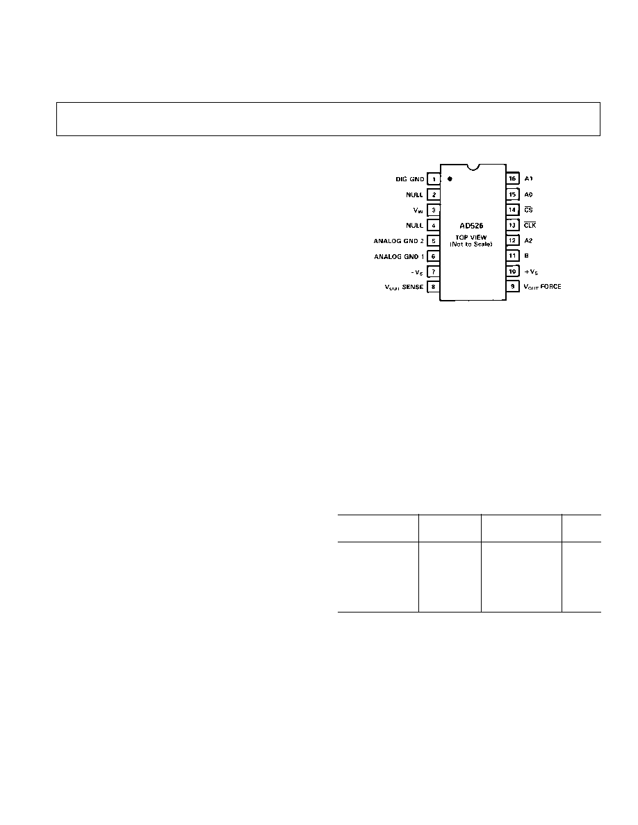
PIN CONFIGURATION
One Technology Way, P.O. Box 9106, Norwood, MA 02062-9106, U.S.A.
Tel: 617/329-4700
Fax: 617/326-8703
APPLICATION HIGHLIGHTS
1. Dynamic Range Extension for ADC Systems: A single
AD526 in conjunction with a 12-bit ADC can provide
96 dB of dynamic range for ADC systems.
2. Gain Ranging Pre-Amps: The AD526 offers complete
digital gain control with precise gains in binary steps from 1
to 16. Additional gains of 32, 64, 128 and 256 are possible
by cascading two AD526s.
ORDERING GUIDE
Temperature
Package
Package
Model
Range
Description
Option
AD526JN
Commercial
16-Pin Plastic DIP
N-16
AD526AD
Industrial
16-Pin Cerdip
D-16
AD526BD
Industrial
16-Pin Cerdip
D-16
AD526CD
Industrial
16-Pin Cerdip
D-16
AD526SD/883B
Military
16-Pin Cerdip
D-16
5962-9089401MEA*
*Refer to official DESC drawing for tested specifications.

AD526J
AD526A
AD526B/S
AD526C
Model
Min
Typ
Max
Min
Typ
Max
Min
Typ
Max
Min
Typ
Max
Units
GAIN
Gain Range
(Digitally Programmable)
1, 2, 4, 8, 16
1, 2, 4, 8, 16
1, 2, 4, 8, 16
1, 2, 4, 8, 16
Gain Error
Gain = 1
0.05
0.02
0.01
0.01
%
Gain = 2
0.05
0.03
0.02
0.01
%
Gain = 4
0.10
0.03
0.02
0.01
%
Gain = 8
0.15
0.07
0.04
0.02
%
Gain = 16
0.15
0.07
0.04
0.02
%
Gain Error Drift
Over Temperature
G = 1
0.5
2.0
0.5
2.0
0.5
2.0
0.5
2.0
ppm/
°
C
G = 2
0.5
2.0
0.5
2.0
0.5
2.0
0.5
2.0
ppm/
°
C
G = 4
0.5
3.0
0.5
3.0
0.5
3.0
0.5
3.0
ppm/
°
C
G = 8
0.5
5.0
0.5
5.0
0.5
5.0
0.5
5.0
ppm/
°
C
G = 16
1.0
5.0
1.0
5.0
1.0
5.0
1.0
5.0
ppm/
°
C
Gain Error (T
MIN
to T
MAX
)
Gain = 1
0.06
0.03
0.02
0.015
%
Gain = 2
0.06
0.04
0.03
0.015
%
Gain = 4
0.12
0.04
0.03
0.015
%
Gain = 8
0.17
0.08
0.05
0.03
%
Gain = 16
0.17
0.08
0.05
0.03
%
Nonlinearity
Gain = 1
0.005
0.005
0.005
0.0035 % FSR
Gain = 2
0.001
0.001
0.001
0.001
% FSR
Gain = 4
0.001
0.001
0.001
0.001
% FSR
Gain = 8
0.001
0.001
0.001
0.001
% FSR
Gain = 16
0.001
0.001
0.001
0.001
% FSR
Nonlinearity (T
MIN
to T
MAX
)
Gain = 1
0.01
0.01
0.01
0.007
% FSR
Gain = 2
0.001
0.001
0.001
0.001
% FSR
Gain = 4
0.001
0.001
0.001
0.001
% FSR
Gain = 8
0.001
0.001
0.001
0.001
% FSR
Gain = 16
0.001
0.001
0.001
0.001
% FSR
VOLTAGE OFFSET, ALL GAINS
Input Offset Voltage
0.4
1.5
0.25
0.7
0.25
0.5
0.25
0.5
mV
Input Offset Voltage Drift Over
Temperature
5
20
3
10
3
10
3
10
µ
V/
°
C
Input Offset Voltage
T
MIN
to T
MAX
2.0
1.0
0.8
0.8
mV
Input Offset Voltage vs. Supply
(V
S
±
10%)
80
80
84
90
dB
INPUT BIAS CURRENT
Over Input Voltage Range
±
10 V
50
150
50
150
50
150
50
150
pA
ANALOG INPUT
CHARACTERISTICS
Voltage Range
(Linear Operation)
10
±
12
10
±
12
10
±
12
10
±
12
V
Capacitance
5
5
5
5
pF
RATED OUTPUT
Voltage
10
±
12
10
±
12
10
±
12
10
±
12
V
Current (V
OUT
=
±
10 V)
±
10
5
±
10
5
±
10
5
±
10
mA
Short-Circuit Current
15
30
15
30
15
30
15
30
mA
DC Output Resistance
0.002
0.002
0.002
0.002
Load Capacitance
(For Stable Operation)
700
700
700
700
pF
NOISE, ALL GAINS
Voltage Noise, RTI
0.1 Hz to 10 Hz
3
3
3
3
µ
V p-p
Voltage Noise Density, RTI
f = 10 Hz
70
70
70
70
nV
Hz
f = 100 Hz
60
60
60
60
nV
Hz
f = 1 kHz
30
30
30
30
nV
Hz
f = 10 kHz
25
25
25
35
nV
Hz
AD526SPECIFICATIONS
(@ V
S
= 15 V, R
L
= 2 k and T
A
= +25 C unless otherwise noted)
REV. C
2

AD526
AD526J
AD526A
AD526B/S
AD526C
Model
Min
Typ
Max
Min
Typ
Max
Min
Typ
Max
Min
Typ
Max
Units
DYNAMIC RESPONSE
3 dB Bandwidth (Small Signal)
G = 1
4.0
4.0
4.0
4.0
MHz
G = 2
2.0
2.0
2.0
2.0
MHz
G = 4
1.5
1.5
1.5
1.5
MHz
G = 8
0.65
0.65
0.65
0.65
MHz
G = 16
0.35
0.35
0.35
0.35
MHz
Signal Settling Time to 0.01%
(
V
OUT
=
±
10 V)
G = 1
2.1
4
2.1
4
2.1
4
2.1
4
µ
s
G = 2
2.5
5
2.5
5
2.5
5
2.5
5
µ
s
G = 4
2.7
5
2.7
5
2.7
5
2.7
5
µ
s
G = 8
3.6
7
3.6
7
3.6
7
3.6
7
µ
s
G = 16
4.1
7
4.1
7
4.1
7
4.1
7
µ
s
Full Power Bandwidth
G = 1, 2, 4
0.10
0.10
0.10
0.10
MHz
G = 8, 16
0.35
0.35
0.35
0.35
MHz
Slew Rate
G = 1, 2, 4
4
6
4
6
4
6
4
6
V/
µ
s
G = 8, 16
18
24
18
24
18
24
18
24
V/
µ
s
DIGITAL INPUTS
(T
MIN
to T
MAX
)
Input Current (V
H
= 5 V)
60
100
140
60
100
140
60
100
140
60
100
140
µ
A
Logic "1"
2
6
2
6
2
6
2
6
V
Logic "0"
0
0.8
0
0.8
0
0.8
0
0.8
V
TIMING
1
(V
L
= 0.2 V, V
H
= 3.7 V)
A0, A1, A2
T
C
50
50
50
50
ns
T
S
30
30
30
30
ns
T
H
30
30
30
30
ns
B
T
C
50
50
50
50
ns
T
S
40
40
40
40
ns
T
H
10
10
10
30
ns
TEMPERATURE RANGE
Specified Performance
0
+70
40
+85
40/55
+85/+125 40
+85
°
C
Storage
65
+125
65
+150
65
+150
65
+150
°
C
POWER SUPPLY
Operating Range
4.5
16.5
4.5
16.5
4.5
16.5
4.5
16.5
V
Positive Supply Current
10
14
10
14
10
14
10
14
mA
Negative Supply Current
10
13
10
13
10
13
10
13
mA
PACKAGE OPTIONS
Plastic (N-16)
AD526JN
Ceramic DIP (D-16)
AD526AD
AD526BD AD526SD
AD526CD
AD526SD/883B
NOTES
1
Refer to Figure 25 for definitions. FSR = Full Scale Range = 20 V. RTI = Referred to Input.
Specifications subject to change without notice.
Specifications shown in boldface are tested on all production units at final electrical test. All min and max specifications are guaranteed, although only those shown in
boldface are tested on all production units.
3
REV. C
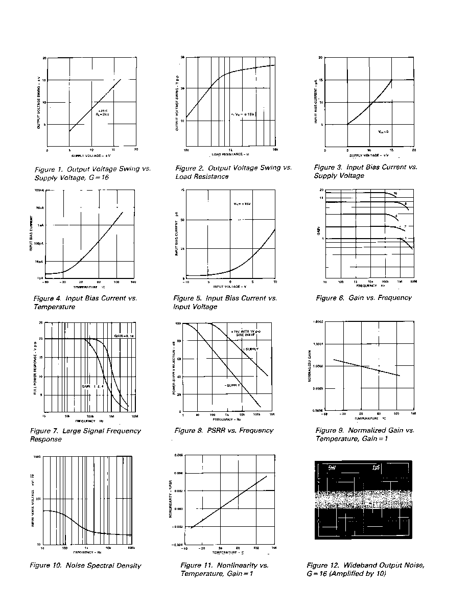
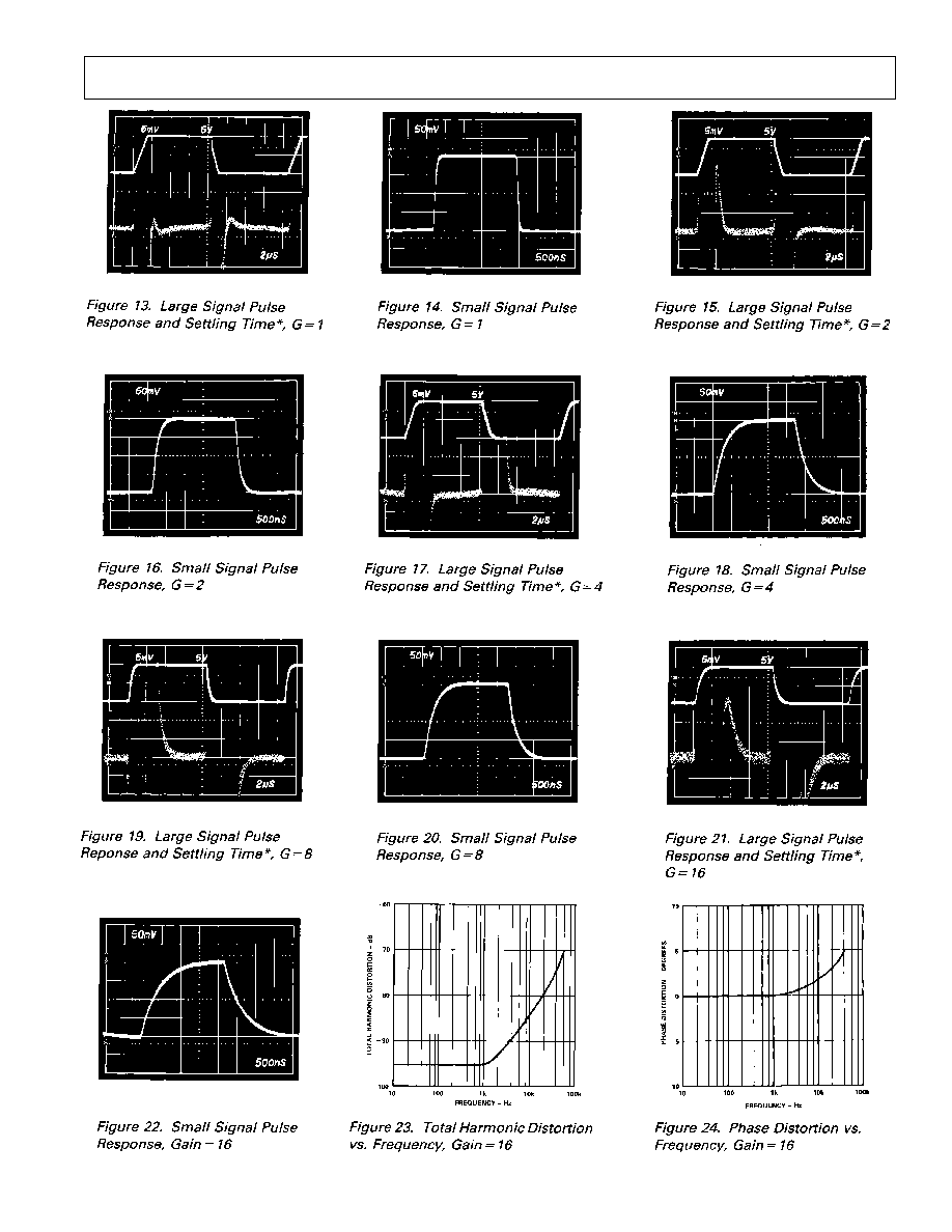
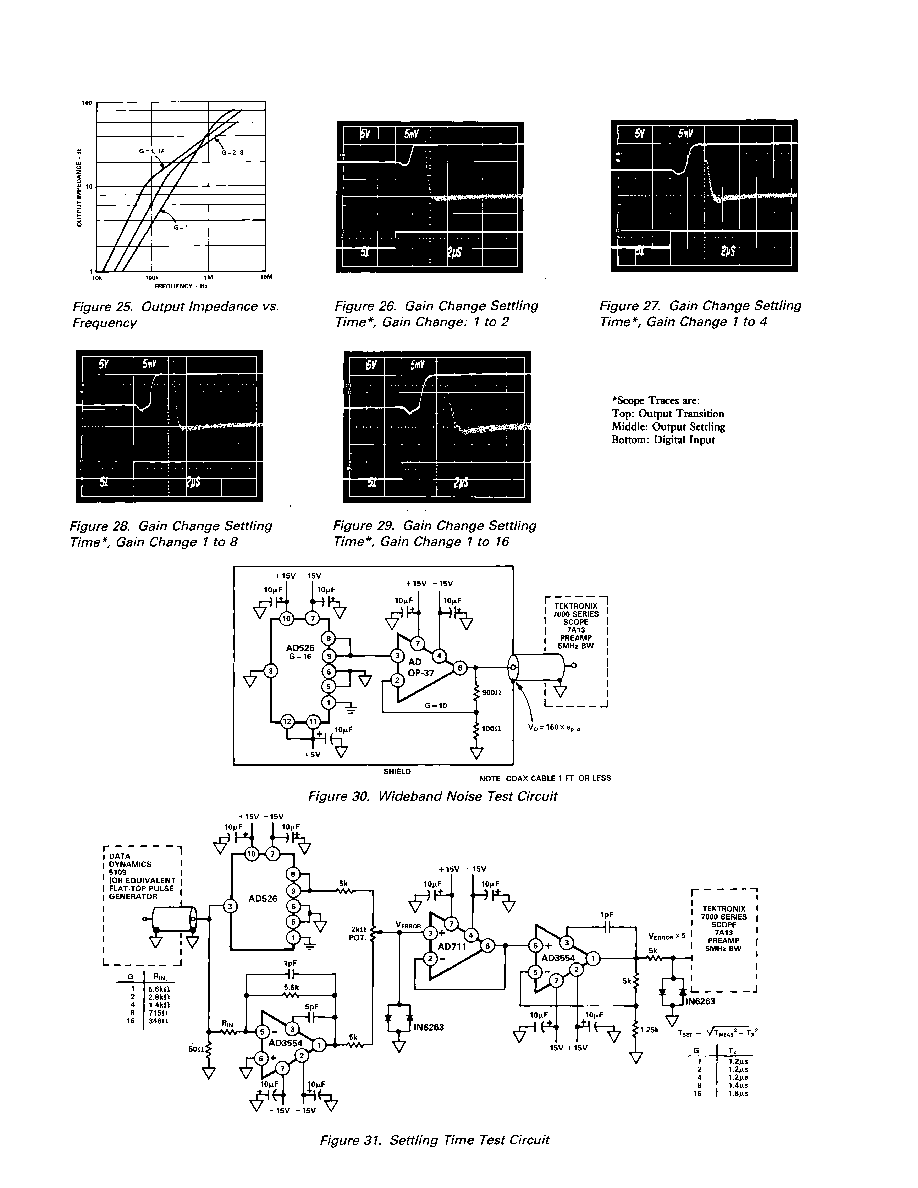
AD526Typical Characteristics
REV. C
4
AD526
REV. C
5
*For Settling Time Traces, 0.01% = 1/2 Vertical Division
AD526
REV. C
6
AD526
REV. C
7
THEORY OF OPERATION
The AD526 is a complete software programmable gain amplifier
(SPGA) implemented monolithically with a drift-trimmed
BiFET amplifier, a laser wafer trimmed resistor network, JFET
analog switches and TTL compatible gain code latches.
A particular gain is selected by applying the appropriate gain
code (see Table I) to the control logic. The control logic turns
on the JFET switch that connects the correct tap on the gain
network to the inverting input of the amplifier; all unselected
JFET gain switches are off (open). The "on" resistance of the
gain switches causes negligible gain error since only the
amplifier's input bias current, which is less than 150 pA, actu-
ally flows through these switches.
The AD526 is capable of storing the gain code, (latched mode),
B, A0, A1, A2, under the direction of control inputs CLK and
CS
. Alternatively, the AD526 can respond directly to gain code
changes if the control inputs are tied low (transparent mode).
For gains of 8 and 16, a fraction of the frequency compensation
capacitance (C1 in Figure 32) is automatically switched out of
the circuit. This increases the amplifier's bandwidth and im-
proves its signal settling time and slew rate.
Figure 32. Simplified Schematic of the AD526
TRANSPARENT MODE OF OPERATION
In the transparent mode of operation, the AD526 will respond
directly to level changes at the gain code inputs (A0, A1, A2) if
B is tied high and both CS and CLK are allowed to float low.
After the gain codes are changed, the AD526's output voltage
typically requires 5.5
µ
s to settle to within 0.01% of the final
value. Figures 26 to 29 show the performance of the AD526 for
positive gain code changes.
Figure 33. Transparent Mode
LATCHED MODE OF OPERATION
The latched mode of operation is shown in Figure 34. When
either CS or CLK go to a logic "1," the gain code (A0, A1, A2,
B) signals are latched into the registers and held until both CS
and CLK return to "0." Unused CS or CLK inputs should be tied
to ground . The CS and CLK inputs are functionally and electri-
cally equivalent.
Figure 34. Latched Mode
AD526
REV. C
8
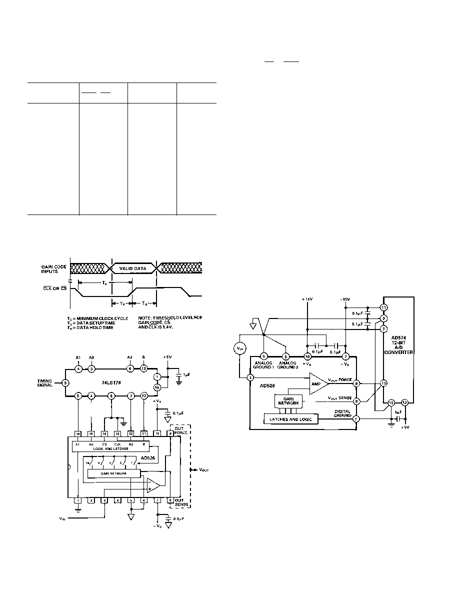
The specifications on page 3 in combination with Figure 35 give
the timing requirements for loading new gain codes.
Figure 35. AD526 Timing
Figure 36. Using an External Latch to Minimize Digital
Feedthrough
TIMING AND CONTROL
Table I. Logic Input Truth Table
Gain Code
Control
Condition
A2 A1 A0 B
CLK
(CS = 0)
Gain
Condition
X
X
X
X
1
Previous State
Latched
0
0
0
1
0
1
Transparent
0
0
1
1
0
2
Transparent
0
1
0
1
0
4
Transparent
0
1
1
1
0
8
Transparent
1
X
X
1
0
16
Transparent
X
X
X
0
0
1
Transparent
X
X
X
0
1
1
Latched
0
0
0
1
1
1
Latched
0
0
1
1
1
2
Latched
0
1
0
1
1
4
Latched
0
1
1
1
1
8
Latched
1
X
X
1
1
16
Latched
NOTE: X = Don't Care.
DIGITAL FEEDTHROUGH
With either CS or CLK or both held high, the AD526 gain state
will remain constant regardless of the transitions at the A0, A1,
A2 or B inputs. However, high speed logic transitions will un-
avoidably feed through to the analog circuitry within the AD526
causing spikes to occur at the signal output.
This feedthrough effect can be completely eliminated by operat-
ing the AD526 in the transparent mode and latching the gain
code in an external bank of latches (Figure 36).
To operate the AD526 using serial inputs, the configuration
shown in Figure 36 can be used with the 74LS174 replaced by a
serial-in/parallel-out latch, such as the 54LS594.
GROUNDING AND BYPASSING
Proper signal and grounding techniques must be applied in
board layout so that specified performance levels of precision
data acquisition components, such as the AD526, are not
degraded.
As is shown in Figure 37, logic and signal grounds should be
separate. By connecting the signal source ground locally to the
AD526 analog ground Pins 5 and 6, gain accuracy of the
AD526 is maintained. This ground connection should not be
corrupted by currents associated with other elements within the
system.
Utilizing the force and sense outputs of the AD526, as shown in
Figure 38, avoids signal drops along etch runs to low impedance
loads.
Figure 37. Grounding and Bypassing
AD526
REV. C
9
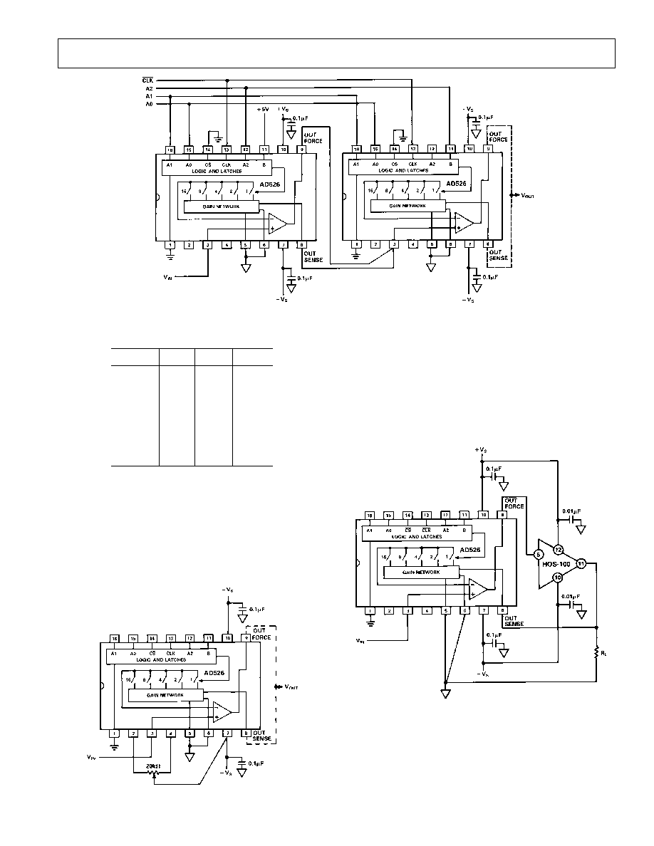
Table II. Logic Table for Figure 38
V
OUT
/V
IN
A2
A1
A0
1
0
0
0
2
0
0
1
4
0
1
0
8
0
1
1
16
1
0
0
32
1
0
1
64
1
1
0
128
1
1
1
OFFSET NULLING
Input voltage offset nulling of the AD526 is best accomplished
at a gain of 16, since the referred-to-input (RTI) offset is ampli-
fied the most at this gain and therefore is most easily trimmed.
The resulting trimmed value of RTI voltage offset typically var-
ies less than 3
µ
V across all gain ranges.
Note that the low input current of the AD526 minimizes RTI
voltage offsets due to source resistance.
Figure 39. Offset Voltage Null Circuit
Figure 38. Cascaded Operation
OUTPUT CURRENT BOOSTER
The AD526 is rated for a full
±
10 V output voltage swing into
2 k
. In some applications, the need exists to drive more cur-
rent into heavier loads. As shown in Figure 40, a high current
booster may be connected "inside the loop" of the SPGA to
provide the required current boost without significantly degrad-
ing overall performance. Nonlinearities, offset and gain inaccu-
racies of the buffer are minimized by the loop gain of the
AD526 output amplifier.
Figure 40. Current Output Boosting
CASCADED OPERATION
A cascade of two AD526s can be used to achieve binarily
weighted gains from 1 to 256. If gains from 1 to 128 are needed,
no additional components are required. This is accomplished by
using the B pin as shown in Figure 38. When the B pin is low,
the AD526 is held in a unity gain stage independent of the other
gain code values.
AD526
REV. C
10
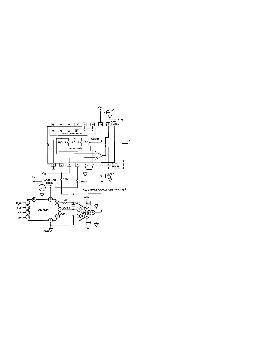
OFFSET NULLING WITH A D/A CONVERTER
Figure 41 shows the AD526 with offset nulling accomplished
with an 8-bit D/A converter (AD7524) circuit instead of the po-
tentiometer shown in Figure 39. The calibration procedure is
the same as before except that instead of adjusting the potenti-
ometer, the D/A converter corrects for the offset error. This
calibration circuit has a number of benefits in addition to elimi-
nating the trimpot. The most significant benefit is that calibra-
tion can be under the control of a microprocessor and therefore
can be implemented as part of an autocalibration scheme. Sec-
ondly, dip switches or RAM can be used to hold the 8-bit word
after its value has been determined. In Figure 42 the offset null
sensitivity, at a gain of 16, is 80
µ
V per LSB of adjustment,
which guarantees dc accuracy to the 16-bit performance level.
Figure 41. Offset Nulling Using a DAC
FLOATING-POINT CONVERSION
High resolution converters are used in systems to obtain high
accuracy, improve system resolution or increase dynamic range.
There are a number of high resolution converters available with
throughput rates of 66.6 kHz that can be purchased as a single
component solution; however in order to achieve higher through-
put rates, alternative conversion techniques must be employed.
A floating point A/D converter can improve both throughput
rate and dynamic range of a system.
In a floating point A/D converter (Figure 42), the output data is
presented as a 16-bit word, the lower 12 bits from the A/D con-
verter form the mantissa and the upper 4 bits from the digital
signal used to set the gain form the exponent. The AD526 pro-
grammable gain amplifier in conjunction with the comparator
circuit scales the input signal to a range between half scale and
full scale for the maximum usable resolution.
The A/D converter diagrammed in Figure 42 consists of a pair
of AD585 sample/hold amplifiers, a flash converter, a five-range
programmable gain amplifier (the AD526) and a fast 12-bit A/D
converter (the AD7572). The floating-point A/D converter
achieves its high throughput rate of 125 kHz by overlapping the
acquisition time of the first sample/hold amplifier and the set-
tling time of the AD526 with the conversion time of the A/D
converter. The first sample/hold amplifier holds the signal for
the flash autoranger, which determines which binary quantum
the input falls within, relative to full scale. Once the AD526 has
settled to the appropriate level, then the second sample/hold
amplifier can be put into hold which holds the amplified signal
while the AD7572 perform its conversion routine. The acquisi-
tion time for the AD585 is 3
µ
s, and the conversion time for the
AD7572 is 5
µ
s for a total of 8
µ
s, or 125 kHz. This performance
relies on the fast settling characteristics of the AD526 after the
flash autoranging (comparator) circuit quantizes the input sig-
nal. A 16-bit register holds the 3-bit output from the flash
autoranger and the 12-bit output of the AD7572.
The A/D converter in Figure 42 has a dynamic range of 96 dB.
The dynamic range of a converter is the ratio of the full-scale
input range to the LSB value. With a floating-point A/D con-
verter the smallest value LSB corresponds to the LSB of the
monolithic converter divided by the maximum gain of the PGA.
The floating point A/D converter has a full-scale range of 5 V, a
maximum gain of 16 V/V from the AD526 and a 12-bit A/D
converter; this produces:
LSB = ([FSR/2
N
]/Gain) = ([5 V/4096]/16) = 76
µ
V. The
dynamic range in dBs is based on the log of the ratio of the
full-scale input range to the LSB; dynamic range = 20 log
(5 V/76
µ
V) = 96 dB.
AD526
REV. C
11
Figure 42. Floating-Point A/D Converter
HIGH ACCURACY A/D CONVERTERS
Very high accuracy and high resolution floating-point A/D con-
verters can be achieved by the incorporation of offset and gain
calibration routines. There are two techniques commonly used
for calibration, a hardware circuit as shown in Figure 43 and/or
a software routine. In this application the microprocessor is
functioning as the autoranging circuit, requiring software over-
head; therefore, a hardware calibration technique was applied
which reduces the software burden. The software is used to set
the gain of the AD526. In operation the signal is converted, and
if the MSB of the AD574 is not equal to a logical 1, the gain is
increased by binary steps, up to the maximum gain. This maxi-
mizes the full-scale range of the conversion process and insures
a wide dynamic range.
The calibration technique uses two point correction, offset and
gain. The hardware is simplified by the use of programmable
magnitude comparators, the 74ALS528s, which can be
"burned" for a particular code. In order to prevent under or
over range hunting during the calibration process, the reference
offset and gain codes should be different from the endpoint
codes. A calibration cycle consists of selecting whether gain or
offset is to be calibrated then selecting the appropriate multi-
plexer channel to apply the reference voltage to the signal chan-
nel. Once the operation has been initiated, the counter, a
74ALS869, drives the D/A converter in a linear fashion provid-
ing a small correction voltage to either the gain or offset trim
point of the AD574. The output of the A/D converter is then
compared to the value preset in the 74ALS528 to determine a
match. Once a match is detected, the 74ALS528 produces a low
going pulse which stops the counter. The code at the D/A con-
verter is latched until the next calibration cycle. Calibration
cycles are under the control of the microprocessor in this appli-
cation and should be implemented only during periods of con-
verter inactivity.
AD526
REV. C
12
PRINTED IN U.S.A.
C1103a92/88
Figure 43. High Accuracy A/D Converter
OUTLINE DIMENSIONS
Dimensions shown in inches and (mm).
16-Pin Plastic
DIP Package (N-16)
16-Pin Sided-Brazed
Ceramic Package (D-16)