 | ÐлекÑÑоннÑй компоненÑ: AD5282 | СкаÑаÑÑ:  PDF PDF  ZIP ZIP |
Äîêóìåíòàöèÿ è îïèñàíèÿ www.docs.chipfind.ru
PRELIMINARY TECHNICAL DATA
a
+15V, I
2
C Compatible
Digital Potentiometers
Preliminary Technical Data
AD5280/AD5282
REV PrE 12 MAR 02
Information furnished by Analog Devices is believed to be accurate and reliable. However, no
responsibility is assumed by Analog Devices for its use; nor for any infringements of patents
or other rights of third parties which may result from its use. No license is granted by
implication or otherwise under any patent or patent rights of Analog Devices.
One Technology Way, P.O. Box 9106,
Norwood, MA 02062-9106 U
.
S
.
A
.
Tel: 781/329-4700 www.analog.com
Fax: 781/326-8703 ©Analog Devices, Inc., 2002
FEATURES
256 Position
AD5280 1-Channel
AD5282 2-Channel (Independently Programmable)
Potentiometer Replacement
20K, 50K, 200K Ohm with TC < 50ppm/ºC
Internal Power ON Mid-Scale Preset
+5 to +15V Single-Supply; ±5.5V Dual-Supply Operation
I
2
C Compatible Interface
APPLICATIONS
Multi-Media, Video & Audio
Communications
Mechanical Potentiometer Replacement
Instrumentation: Gain, Offset Adjustment
Programmable Voltage to Current Conversion
Line Impedance Matching
GENERAL DESCRIPTION
The AD5280/AD5282 provides a single/dual channel, 256 position
digitally-controlled variable resistor (VR) device. These devices
perform the same electronic adjustment function as a
potentiometer, trimmer or variable resistor. Each VR offers a
completely programmable value of resistance, between the A
terminal and the wiper, or the B terminal and the wiper. The fixed
A-to-B terminal resistance of 20, 50 or 200K ohms has a 1%
channel-to-channel matching tolerance with a nominal temperature
coefficient of 30 ppm/°C.
Wiper Position programming defaults to midscale at system power
ON. Once powered the VR wiper position is programmed by a I
2
C
compatible 2-wire serial data interface. Both parts have two
programmable logic outputs available to drive digital loads, gates,
LED drivers, analog switches, etc.
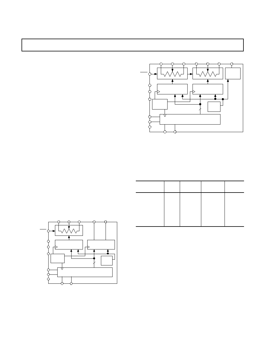
FUNCTIONAL BLOCK DIAGRAMS
RDAC1 REGISTER
ADDRESS
DECODE
SERIAL INPUT REGISTER
PWR ON
RESET
SDA
SCL
V
SS
V
DD
GND
A
1
W
1
B
1
AD5280
8
SHDN
RDAC2 REGISTER
O
1
R
R
V
L
AD0
AD1
O
2
RDAC1 REGISTER
ADDRESS
DECODE
SERIAL INPUT REGISTER
PWR ON
RESET
SDA
SCL
V
SS
V
DD
GND
A
1
W
1
B
1
AD5282
8
SHDN
RDAC2 REGISTER
A
2
W
2
B
2
R
R
V
L
AD0
AD1
OUTPUT
REGISTER
O
1
R
The AD5280/AD5282 are available in ultra compact surface mount
thin TSSOP-14/-16 packages. All parts are guaranteed to operate
over the extended industrial temperature range of -40°C to +85°C.
For 3-wire, SPI compatible interface applications, see
AD5203/AD5204/AD5206/AD7376/AD8400/AD8402/AD8403/
AD5260/AD5262/AD5200/AD5201 products.
ORDERING GUIDE
Kilo
Package
Package
Model Ohms
Temp
Description
Option
AD5280BRU20 20
-40/+85°C TSSOP-14 RU-14
AD5280BRU50 50
-40/+85°C TSSOP-14 RU-14
AD5280BRU200 200
-40/+85°C TSSOP-14
RU-14
AD5282BRU20 20
-40/+85°C TSSOP-16 RU-16
AD5282BRU50 50
-40/+85°C TSSOP-16 RU-16
AD5282BRU200 200
-40/+85°C TSSOP-16
RU-16
The AD5280/AD5282 die size is 75 mil X 120 mil, 9,000 sq. mil.
Contains xxx transistors. Patent Number xxx applies.

PRELIMINARY TECHNICAL DATA
AD5280/AD5282
2 REV PrE 12 MAR 02
Information contained in this Product Concept Data Sheet describes a product in the early definition stage. There is no guarantee that the information contained here will become a final
product in its present form. For latest information contact Walt Heinzer/Analog Devices, Santa Clara, CA. TEL 408 382-3107; FAX 408 382-2721; email; walt.heinzer@analog.com
ELECTRICAL CHARACTERISTICS 20K, 50K, 200K OHM VERSION
(V
DD
=
+5
V, V
SS
= -
5
V, V
LOGIC
=
+5
V,
V
A
= +V
DD
, V
B
= 0V, -40°C < T
A
< +85°C unless otherwise noted.)
Parameter Symbol
Conditions
Min
Typ
1
Max
Units
DC CHARACTERISTICS RHEOSTAT MODE Specifications apply to all VRs
Resistor Differential NL
2
R-DNL
R
WB
, V
A
=NC
-1
±0.4
+1
LSB
Resistor Nonlinearity
2
R-INL
R
WB
, V
A
=NC
-1
±0.5
+1
LSB
Nominal resistor tolerance
3
R T
A
= 25°C
-30
30
%
Resistance Temperature Coefficient
R
AB
/
T V
AB
= V
DD
, Wiper = No Connect
30
ppm/°C
Wiper Resistance
R
W
I
W
= V
DD
/R, V
DD
= +3V or +5V
40
100
DC CHARACTERISTICS POTENTIOMETER DIVIDER MODE Specifications apply to all VRs
Resolution N
8
Bits
Integral Nonlinearity
4
INL
R
AB
=20K
, 50K
1
±0.5
+1
LSB
Integral Nonlinearity
4
INL
R
AB
=200K
2
±0.5
+2
LSB
Differential Nonlinearity
4
DNL
1
±0.4
+1
LSB
Voltage Divider Temperature Coefficient
V
W
/
T
Code = 80
H
5 ppm/°C
Full-Scale Error
V
WFSE
Code = FF
H
1
-0.5
+0
LSB
Zero-Scale Error
V
WZSE
Code = 00
H
0
+0.5
+1
LSB
RESISTOR TERMINALS
Voltage Range
5
V
A,B,W
V
SS
V
DD
V
Capacitance
6
A, B
C
A,B
f = 1 MHz, measured to GND, Code = 80
H
45
pF
Capacitance
6
W
C
W
f = 1 MHz, measured to GND, Code = 80
H
60
pF
Common Mode Leakage
I
CM
V
A
= V
B
= V
W
1
nA
DIGITAL INPUTS
Input Logic High
V
IH
SDA & SCL
0.7V
LOGIC
V
LOGIC
+0.5 V
Input Logic Low
V
IL
SDA & SCL
-0.5
0.3V
LOGIC
V
Input Logic High
V
IH
AD0 & AD1
2.4
V
LOGIC
V
Input Logic Low
V
IL
AD0 & AD1
0
0.8
V
Input Logic High
V
IH
V
LOGIC
= +3V, AD0 & AD1
2.1
V
LOGIC
V
Input Logic Low
V
IL
V
LOGIC
= +3V, AD0 & AD1
0
0.6
V
Input Current
I
IL
V
IN
= 0V or +5V
±1
µA
Input Capacitance
6
C
IL
3
pF
DIGITAL Output
O1, O2
V
OH
I
OH
=0.4mA
2.4
5.5
V
O1, O2
V
OL
I
OL
=-1.6mA
0
0.4
V
SDA V
OL
I
OL
= -6mA
0.6
V
SDA V
OL
I
OL
= -3mA
0.4
V
Three-State Leakage Current
I
OZ
V
IN
= 0V or +5V
±1
µA
Output Capacitance
6
C
OZ
3 8
pF
POWER SUPPLIES
Logic Supply
V
LOGIC
+2.7 +5.5
V
Power Single-Supply Range
V
DD RANGE
V
SS
= 0V
+5
+15
V
Power Dual-Supply Range
V
DD/SS RANGE
±4.5 ±5.5
V
Logic Supply Current
I
LOGIC
V
LOGIC
= +5V
10
µA
Positive Supply Current
I
DD
V
IH
= +5V or V
IL
= 0V
20
60
µA
Negative Supply Current
I
SS
20
60
µA
Power Dissipation
10
P
DISS
V
IH
= +5V or V
IL
= 0V, V
DD
= +5V, V
SS
= -5V
0.2
0.6
mW
Power Supply Sensitivity
PSS
0.05
0.015
%/%

PRELIMINARY TECHNICAL DATA
AD5280/AD5282
REV PrE 12 MAR 02
3
Information contained in this Product Concept Data Sheet describes a product in the early definition stage. There is no guarantee that the information contained here will become a final
product in its present form. For latest information contact Walt Heinzer/Analog Devices, Santa Clara, CA. TEL 408 382-3107; FAX 408 382-2721; email; walt.heinzer@analog.com
ELECTRICAL CHARACTERISTICS 20K, 50K, 200K OHM VERSION
(V
DD
=
+5
V, V
SS
= -
5
V, V
LOGIC
=
+5
V,
V
A
= +V
DD
, V
B
= 0V, -40°C < T
A
< +85°C unless otherwise noted.)
Parameter Symbol
Conditions
Min
Typ
1
Max
Units
DYNAMIC CHARACTERISTICS
6,9,11
Bandwidth 3dB
BW_20K
R
AB
= 20K
, Code = 80
H
650
kHz
BW_50K
R
AB
= 50K
, Code = 80
H
142
kHz
BW_200K
R
AB
= 200K
, Code = 80
H
69
kHz
Total Harmonic Distortion
THD
W
V
A
=1Vrms + 2V dc, V
B
= 2V DC, f=1KHz
0.005
%
V
W
Settling Time
t
S
V
A
= V
DD
, V
B
=0V, ±1 LSB error band
2
µs
Resistor Noise Voltage
e
N_WB
R
WB
= 10K
, f = 1KHz
14
nV
Hz
INTERFACE TIMING CHARACTERISTICS applies to all parts(Notes 6,12)
SCL Clock Frequency
f
SCL
0 400
KHz
t
BUF
Bus free time between
STOP & START
t1
1.3
µs
t
HD;STA
Hold Time (repeated START)
t2
After this period the first clock pulse is generated
0.6
µs
t
LOW
Low Period of SCL Clock
t3
1.3
µs
t
HIGH
High Period of SCL Clock
t4
0.6
µs
t
SU;STA
Setup Time For START Condition t5
0.6
µs
t
HD;DAT
Data Hold Time
t6
0
0.9
µs
t
SU;DAT
Data Setup Time
t7
100
ns
t
F
Fall Time of both SDA & SCL signals
t8
300
ns
t
R
Rise Time of both SDA & SCL signals
t9
300
ns
t
SU;STO
Setup time for STOP Condition
t10
0.6
µs
NOTES:
1.
Typicals represent average readings at +25°C, V
DD
= +5V, V
SS
= -5V.
2.
Resistor position nonlinearity error R-INL is the deviation from an ideal value measured between the maximum resistance and the minimum resistance wiper positions. R-DNL measures the
relative step change from ideal between successive tap positions. Parts are guaranteed monotonic.
3. V
AB
= V
DD
, Wiper (V
W
) = No connect
4.
INL and DNL are measured at V
W
with the RDAC configured as a potentiometer divider similar to a voltage output D/A converter. V
A
= V
DD
and V
B
= 0V.
DNL specification limits of ±1LSB maximum are Guaranteed Monotonic operating conditions.
5.
Resistor terminals A,B,W have no limitations on polarity with respect to each other.
6.
Guaranteed by design and not subject to production test.
9.
Bandwidth, noise and settling time are dependent on the terminal resistance value chosen. The lowest R value results in the fastest settling time and highest bandwidth. The highest R value
result in the minimum overall power consumption.
10. PDISS is calculated from (IDD x VDD). CMOS logic level inputs result in minimum power dissipation.
11.
All dynamic characteristics use V
DD
= +5V.
12.
See timing diagram for location of measured values.
PRELIMINARY TECHNICAL DATA
AD5280/AD5282
4 REV PrE 12 MAR 02
Information contained in this Product Concept Data Sheet describes a product in the early definition stage. There is no guarantee that the information contained here will become a final
product in its present form. For latest information contact Walt Heinzer/Analog Devices, Santa Clara, CA. TEL 408 382-3107; FAX 408 382-2721; email; walt.heinzer@analog.com
ABSOLUTE MAXIMUM RATINGS (T
A
= +25°C, unless
otherwise noted)
V
DD
to GND ............................................................. -0.3, +15V
V
SS
to GND .................................................................. 0V, -7V
V
DD
to V
SS
...................................................................... +15V
V
A
, V
B
, V
W
to GND...................................................V
SS
, V
DD
A
X
B
X
, A
X
W
X
, B
X
W
X
.........................................±20mA
Digital Input Voltage to GND.........................................0V, 7V
Operating Temperature Range ...........................-40°C to +85°C
Thermal Resistance
*
JA,
TSSOP-14 ........................................................206°C/W
TSSOP-16 ........................................................180°C/W
Maximum Junction Temperature (T
J MAX
) .................... +150°C
Storage Temperature ........................................-65°C to +150°C
Lead Temperature
RU-14, RU-16 (Vapor Phase, 60 sec) ....................... +215°C
RU-14, RU-16 (Infrared, 15 sec) .............................. +220°C
*
Package Power Dissipation (TJMAX - TA) /
JA
AD5280 PIN CONFIGURATION
A
W
B
V
DD
SHDN
SHDN
SHDN
SHDN
SCL
SDA
O1
V
L
O2
V
SS
GND
AD1
AD0
14
13
12
11
10
9
8
1
2
3
4
5
6
7
AD5282 PIN CONFIGURATION
O1
A1
W1
B1
V
DD
SHDN
SHDN
SHDN
SHDN
SCL
SDA
A2
W2
B2
V
L
V
SS
GND
AD1
AD0
16
15
14
13
12
11
10
9
1
2
3
4
5
6
7
8
TABLE 1: AD5280 PIN Function Descriptions
Pin Name
Description
1
A
Resistor terminal A
2
W
Wiper terminal W
3
B
Resistor terminal B
4 V
DD
Positive power supply, specified for
operation from +5 to +15V.
5
SHDN
Active Low, Asynchronous connection of
the wiper W to terminal B, and open
circuit of terminal A. RDAC register
contents unchanged.
6
SCL
Serial Clock Input
7
SDA
Serial Data Input/Output
8
AD0
Programmable address bit for multiple
package decoding. Bits AD0 & AD1
provide 4 possible addresses.
9
AD1
Programmable address bit for multiple
package decoding. Bits AD0 & AD1
provide 4 possible addresses.
10 GND Common
Ground
11 V
SS
Negative power supply, specified for
operation from 0 to -5V
12
O2
Logic Output terminal O2
13 V
L
Logic Supply Voltage, needs to be same
voltage as the digital logic controlling the
AD5280.
14
O1
Logic Output terminal O1
PRELIMINARY TECHNICAL DATA
AD5280/AD5282
REV PrE 12 MAR 02
5
Information contained in this Product Concept Data Sheet describes a product in the early definition stage. There is no guarantee that the information contained here will become a final
product in its present form. For latest information contact Walt Heinzer/Analog Devices, Santa Clara, CA. TEL 408 382-3107; FAX 408 382-2721; email; walt.heinzer@analog.com
TABLE 2: AD5282 PIN Function Descriptions
Pin Name
Description
1
O1
Logic Output terminal O1
2 A
1
Resistor terminal A
1
3 W
1
Wiper terminal W
1
4 B
1
Resistor terminal B
1
5 V
DD
Positive power supply, specified for
operation from +5 to +15V.
6
SHDN
Active Low, Asynchronous connection of
the wiper W to terminal B, and open
circuit of terminal A. RDAC register
contents unchanged.
7
SCL
Serial Clock Input
8
SDA
Serial Data Input/Output
9
AD0
Programmable address bit for multiple
package decoding. Bits AD0 & AD1
provide 4 possible addresses.
10
AD1
Programmable address bit for multiple
package decoding. Bits AD0 & AD1
provide 4 possible addresses.
11 GND Common
Ground
12 V
SS
Negative power supply, specified for
operation from 0 to -5V
13 V
L
Logic Supply Voltage, needs to be same
voltage as the digital logic controlling the
AD5282.
14 B
2
Resistor terminal B
2
15 W
2
Wiper terminal W
2
16 A
2
Resistor terminal A
2
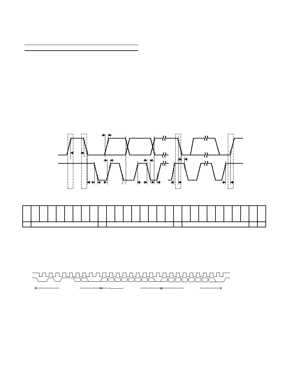
t
4
SDA
SCL
P
S
Sr
P
t
1
t
2
t
3
t
5
t
6
t
7
t
8
t
8
t
9
t
10
Figure 1. Detail Timing Diagram
Data of AD5280/AD5282 is accepted from the I
2
C bus in the following serial format:
S 0 1 0 1 1 A
D
1
A
D
0
R/
W
W
W
W
A
A
A
A
A/
B
R
S
S
D
O
1
O
2
X X X A D
7
D
6
D
5
D
4
D
3
D
2
D
1
D
0
A P
Slave Address Byte
Instruction Byte
Data Byte
Where:
S = Start Condition
P = Stop Condition
A = Acknowledge
X = Don't Care
AD1, AD0 = Package pin programmable address bits
R/W
W
W
W= Read Enable at High and Write Enable at Low
A
A
A
A/B = RDAC sub address select. "Zero" for RDAC1 and "One" for RDAC2
SD = Shutdown, same as SHDN pin operation except inverse logic
O2, O1 = Output logic pin latched values
D7,D6,D5,D4,D3,D2,D1,D0 = Data Bits
SCL
SDA
1
9
1
0
1
1
0
AD0
AD1
R/
W
ACK. BY
AD5280
D7
D6
D5
D3
D4
D0
D1
D2
1
9
ACK. BY
AD5280
A/
B
RS
SD
O2
O1
X
X
X
1
9
ACK. BY
AD5280
FRAME 1
Slave Address Byte
START BY
MASTER
FRAME 2
Instruction Byte
FRAME 3
Data Byte
Figure 2. Writing to the RDAC Register
PRELIMINARY TECHNICAL DATA
AD5280/AD5282
6 REV PrE 12 MAR 02
Information contained in this Product Concept Data Sheet describes a product in the early definition stage. There is no guarantee that the information contained here will become a final
product in its present form. For latest information contact Walt Heinzer/Analog Devices, Santa Clara, CA. TEL 408 382-3107; FAX 408 382-2721; email; walt.heinzer@analog.com
SCL
SDA
1
9
1
0
1
1
0
AD0
AD1
R/
W
ACK. BY
AD5280
1
9
D7
D6
D5
D3
D4
D0
D1
D2
NO ACK.
BY MASTER
FRAME 1
Slave Address Byte
START BY
MASTER
FRAME 2
Data From Select ed
RDAC Regis ter
STOP BY
MASTER
Figure 3. Reading Data from a Previously Selected RDAC Register
OPERATION
The AD5280/AD5282 provides a single/dual channel, 256-
position digitally-controlled variable resistor (VR) device. The
terms VR and RDAC are used interchangeably throughout this
documentation. To program the VR settings, refer to the Digital
Interface section. Both parts have an internal power ON preset
that places the wiper in mid scale during power on, which
simplifies the fault condition recovery at power up. In addition,
the shutdown SHDN pin of AD5280/AD5282 places the RDAC
in a zero power consumption state where terminal A is open
circuited and the wiper W is connected to terminal B, resulting
in only leakage currents being consumed in the VR structure. In
shutdown mode the VR latch settings are maintained, so that,
returning to operational mode from power shutdown, the VR
settings return to their previous resistance values.
RS
D5
D4
D3
D2
D1
D0
RDAC
LATCH
&
DECODER
SHDN
Ax
Bx
Wx
RS
RS
RS
D6
D7
Figure 4. AD5280/AD5282 Equivalent RDAC Circuit
PROGRAMMING THE VARIABLE RESISTOR
Rheostat Operation
The nominal resistance of the RDAC between terminals A and B
are available in 20K
, 50K
, and 200K
. The final three
digits of the part number determine the nominal resistance
value, e.g. 20K
= 20; 50K
= 50; 200K
= 200. The
nominal resistance (R
AB
) of the VR has 256 contact points
accessed by the wiper terminal, plus the B terminal contact. The
eight bit data in the RDAC latch is decoded to select one of the
256 possible settings. Assume a 20K
part is used, the wiper's
first connection starts at the B terminal for data 00
H
. Since there
is a 60
wiper contact resistance, such connection yields a
minimum of 60
resistance between terminals W and B. The
second connection
is the first tap point corresponds to 138
(R
WB
= R
AB
/256 + R
W
= 78
+60
) for data 01
H
. The third
connection is the next tap point representing 216
(78x2+60)
for data 02
H
and so on. Each LSB data value increase moves the
wiper up the resistor ladder until the last tap point is reached at
19982
[R
AB
1LSB+R
W
]. The wiper does not directly connect
to the B terminal. See Figure 4 for a simplified diagram of the
equivalent RDAC circuit.
The general equation determining the digitally programmed
output resistance between W and B is:
1
eqn.
256
)
(
W
AB
WB
R
R
D
D
R
+
=
where D is the decimal equivalent of the binary code which is
loaded in the 8-bit RDAC register, and R
AB
is the nominal end-
to-end resistance.
For example, R
AB
=20K
, when V
B
= 0V and Aterminal is open
circuit, the following output resistance values R
WB
will be set for
the following RDAC latch codes. Result will be the same if
terminal A is tied to W:
D R
WB
Output State
(DEC) (
)
256 19982
Full-Scale (R
AB
- 1LSB + R
W
)
128 10060
Mid-Scale
1 138
1
LSB
0 60
Zero-Scale (Wiper contact resistance)
Note that in the zero-scale condition a finite wiper resistance of
60
is present. Care should be taken to limit the current flow
between W and B in this state to a maximum current of no more
than 5mA. Otherwise, degradation or possible destruction of the
internal switch contact can occur.
Similar to the mechanical potentiometer, the resistance of the
RDAC between the wiper W and terminal A also produces a
digitally controlled resistance R
WA
. When these terminals are
used the Bterminal should be let open or tied to the wiper
terminal. Setting the resistance value for R
WA
starts at a
maximum value of resistance and decreases as the data loaded in
the latch is increased in value. The general equation for this
operation is:
2
eqn.
256
256
)
(
W
AB
WA
R
R
D
D
R
+
-
=

PRELIMINARY TECHNICAL DATA
AD5280/AD5282
REV PrE 12 MAR 02
7
Information contained in this Product Concept Data Sheet describes a product in the early definition stage. There is no guarantee that the information contained here will become a final
product in its present form. For latest information contact Walt Heinzer/Analog Devices, Santa Clara, CA. TEL 408 382-3107; FAX 408 382-2721; email; walt.heinzer@analog.com
For example, R
AB
=20K
, when V
A
= 0V and Bterminal is open
circuit, the following output resistance R
WA
will be set for the
following RDAC latch codes. Result will be the same if terminal
B is tied to W:
D R
WA
Output State
(DEC) (
)
256 60 Full-Scale
128 10060
Mid-Scale
1 19982
1
LSB
0 20060
Zero-Scale
The typical distribution of the nominal resistance R
AB
from
channel-to-channel matches within ±1%. Device to device
matching is process lot dependent and is possible to have ±30%
variation. Since the resistance element is processed in thin film
technology, the change in R
AB
with temperature has a 30
ppm/°C temperature coefficient.
PROGRAMMING THE POTENTIOMETER DIVIDER
Voltage Output Operation
The digital potentiometer easily generates output voltages at
wiper-to-B and wiper-to-A to be proportional to the input
voltage at A-to-B. Let's ignore the effect of the wiper resistance
at the moment. For example connecting Aterminal to +5V and
Bterminal to ground produces an output voltage at the wiper-
to-B starting at zero volts up to 1 LSB less than +5V. Each LSB
of voltage is equal to the voltage applied across terminal AB
divided by the 256 position of the potentiometer divider. Since
AD5280/AD5282 can be supplied by dual supplies, the general
equation defining the output voltage at V
W
with respect to
ground for any given input voltage applied to terminals AB is:
3
eqn.
256
256
256
)
(
B
A
W
V
D
V
D
D
V
-
+
=
where D is decimal equivalent of the binary code which is
loaded in the 8-bit RDAC register.
Operation of the digital potentiometer in the divider mode
results in a more accurate operation over temperature. Unlike
the rheostat mode, the output voltage is dependent on the ratio
of the internal resistors R
WA
and R
WB
and not the absolute values,
therefore, the temperature drift reduces to 5ppm/°C.
DIGITAL INTERFACE
2-WIRE SERIAL BUS
The AD5280/AD5282 are controlled via an I
2
C compatible
serial bus. The RDACs are connected to this bus as slave
devices.
Referring from Figures 2 and 3, the first byte of
AD5280/AD5282 is a Slave Address Byte. It has a 7-bit slave
address and a R/W bit. The 5 MSBs are 01011 and the following
2 bits are determined by the state of the AD0 and AD1 pins of
the device. AD0 and AD1 allow the user to use up to four of
these devices on one bus.
The 2-wire I
2
C serial bus protocol operates as follows:
1. The master initiates data transfer by establishing a START
condition, which is when a high-to-low transition on the
SDA line occurs while SCL is high, Figure 2. The
following byte is the Slave Address Byte which consists of
the 7-bit slave address followed by an R/W bit (this bit
determines whether data will be read from or written to the
slave device).
The slave whose address corresponds to the transmitted
address responds by pulling the SDA line low during the
ninth clock pulse (this is termed the Acknowledge bit). At
this stage, all other devices on the bus remain idle while the
selected device waits for data to be written to or read from
its serial register. If the R/W bit is high, the master will read
from the slave device. On the other hand, if the R/W bit is
low, the master will write to the slave device.
2. A Write operation contains an extra Instruction Byte more
than the Read operation. Such Instruction Byte in Write
mode follows the Slave Address Byte. The MSB of the
Instruction Byte labeled
A/B is the RDAC sub-address
select. A "low" select RDAC1 and a "high" selects RDAC2
for dual channel AD5282. The 2
nd
MSB RS is the Mid-
scale reset. A logic high of this bit moves the wiper of a
selected RDAC to the center tap where R
WA
=R
WB
. The 3
rd
MSB SD is a shutdown bit. A logic high causes the RDAC
open circuit at terminal A while shorting wiper to terminal
B. This operation yields almost a zero Ohm in rheostat
mode or zero volt in potentiometer mode. This SD bit
serves the same function as the SHDN pin except it reacts in
active low. The following two bits are O2 and O1. They are
extra programmable logic output that users can make use of
them by driving other digital loads, logic gates, LED
drivers, and analog switches, etc. The 3 LSBs are DON'T
CARE. See Figure 2.
3. After acknowledged the Instruction Byte, the last byte in
Write mode is the Data Byte. Data is transmitted over the
serial bus in sequences of nine clock pulses (eight data bits
followed by an "Acknowledge" bit). The transitions on the
SDA line must occur during the low period of SCL and
remain stable during the high period of SCL, Figure 1.
4. In Read mode, the Data Byte goes right after the
acknowledgment of the Slave Address Byte. Data is
transmitted over the serial bus in sequences of nine clock
pulses (slight difference with the Write mode, there are
eight data bits followed by a "No Acknowledge" bit).
Similarly, the transitions on the SDA line must occur
during the low period of SCL and remain stable during the
high period of SCL.
5. When all data bits have been read or written, a STOP
condition is established by the master. A STOP condition is
defined as a low-to-high transition on the SDA line while
SCL is high. In Write mode, the master will pull the SDA
line high during the 10
th
clock pulse to establish a STOP
PRELIMINARY TECHNICAL DATA
AD5280/AD5282
8 REV PrE 12 MAR 02
Information contained in this Product Concept Data Sheet describes a product in the early definition stage. There is no guarantee that the information contained here will become a final
product in its present form. For latest information contact Walt Heinzer/Analog Devices, Santa Clara, CA. TEL 408 382-3107; FAX 408 382-2721; email; walt.heinzer@analog.com
condition, Figure 2. In Read mode, the master will issue a
No Acknowledge for the 9
th
clock pulse (i.e., the SDA line
remains high). The master will then bring the SDA line low
before the 10
th
clock pulse which goes high to establish a
STOP condition, Figure 3.
A repeated Write function gives the user flexibility to update the
RDAC output a number of times after addressing and instructing
the part only once. During the Write cycle, each Data byte will
update the RDAC output. For example, after the RDAC has
acknowledged its Slave Address and Instruction Bytes, the
RDAC output will update after these two bytes. If another byte
is written to the RDAC while it is still addressed to a specific
slave device with the same instruction, this byte will update the
output of the selected slave device. If different instructions are
needed, the Write mode has to start with a new Slave Address,
Instruction, and Data Bytes again. Similarly, a repeated Read
function of the RDAC is also allowed.
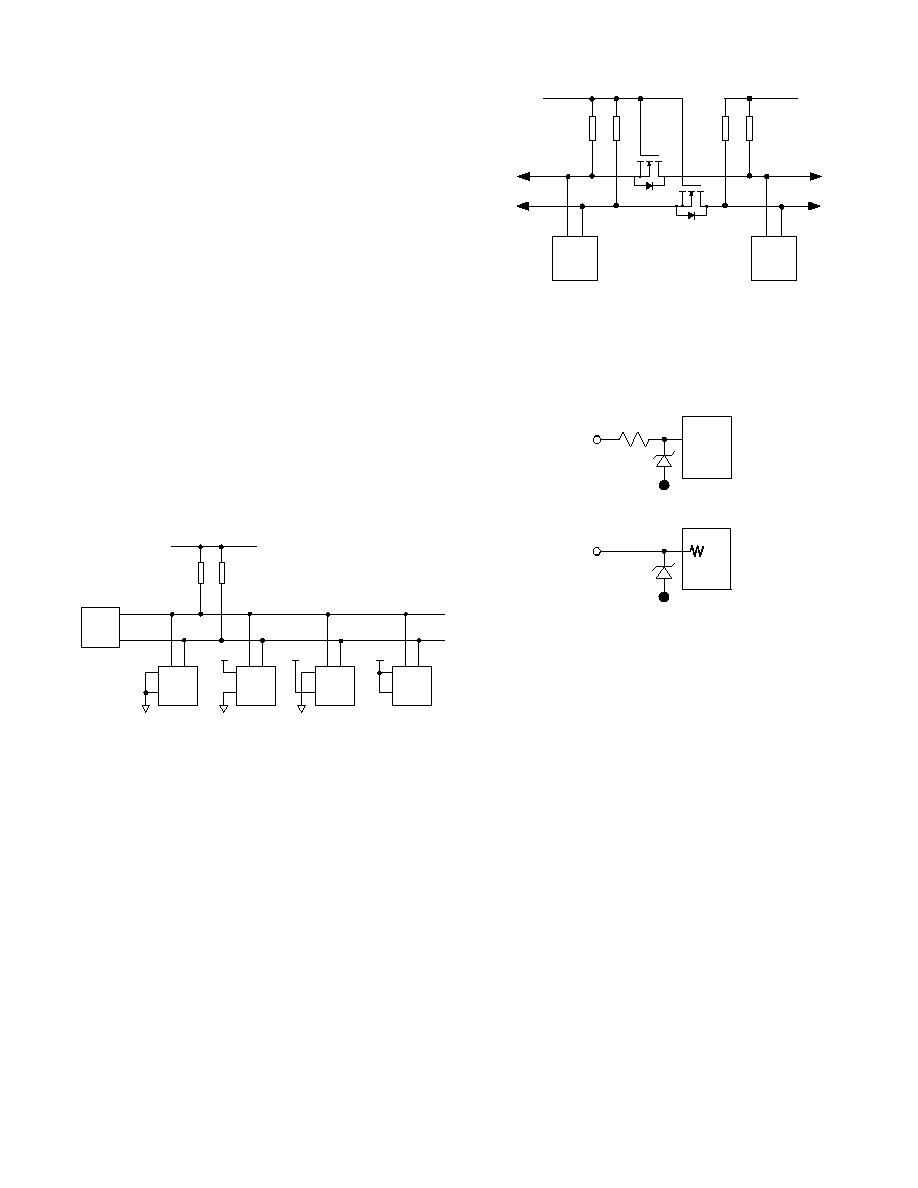
MULTIPLE DEVICES ON ONE BUS
Figure 5 shows four AD5282 devices on the same serial bus.
Each has a different slave address sine the state of their AD0 and
AD1 pins are different. This allows each RDAC within each
device to be written to or read from independently. The master
device output bus line drivers are open-drain pull downs in a
fully I
2
C compatible interface.
SDA SCL
AD5282
AD1
AD0
MASTER
SDA
SCL
Rp
Rp
+5V
SDA SCL
AD5282
AD1
AD0
SDA SCL
AD5282
AD1
AD0
SDA SCL
AD5282
AD1
AD0
VDD
VDD
VDD
Figure 5. Multiple AD5282 Devices on One Bus
LEVEL SHIFT FOR BI-DIRECTIONAL INTERFACE
While most old systems may be operated at one voltage, a new
component may be optimized at another. When two systems
operate the same signal at two different voltages, proper method
of level shifting is needed. For instance, one can use a 3.3V
E
2
PROM to interface with a 5V digital potentiometer. A level
shift scheme is needed in order to enable a bi-directional
communication so that the setting of the digital potentiometer
can be stored to and retrieved from the E
2
PROM. Figure 6
shows one of the techniques. M1 and M2 can be N-Ch FETs
2N7002 or low threshold FDV301N if V
DD
falls below 2.5V.
3.3V
E2PROM
5V
AD5282
SDA1
SCL1
SDA2
SCL2
Rp
Rp
Rp
Rp
VDD1 = 3.3V
VDD2 = 5V
D
D
S
S
G
G
M1
M2
Figure 6. Level Shift for different potential operation.
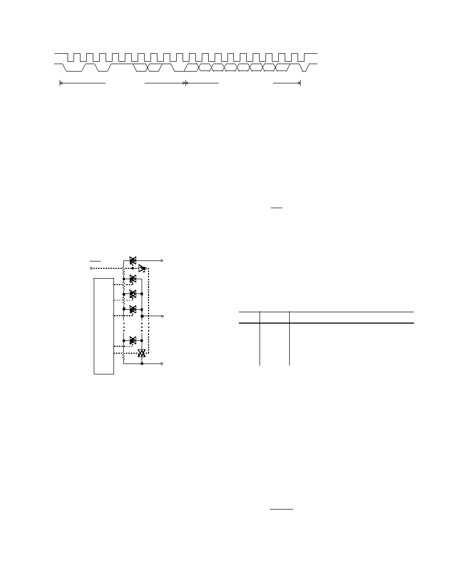
All digital inputs are protected with a series input resistor and
parallel Zener ESD structures shown in figure 7. Applies to
digital input pins SDA, SCL, and SHDN
.
V
SS
LOGIC
340
Figure 7. ESD Protection of digital pins
A,B,W
VSS
Figure 8. ESD Protection of Resistor Terminals
PRELIMINARY TECHNICAL DATA
AD5280/AD5282
REV PrE 12 MAR 02
9
Information contained in this Product Concept Data Sheet describes a product in the early definition stage. There is no guarantee that the information contained here will become a final
product in its present form. For latest information contact Walt Heinzer/Analog Devices, Santa Clara, CA. TEL 408 382-3107; FAX 408 382-2721; email; walt.heinzer@analog.com
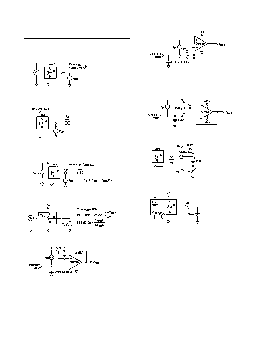
TEST CIRCUITS
Figures 9 to 17 define the test conditions used in product specification
table.
Figure 9. Potentiometer Divider Nonlinearity error test circuit
(INL, DNL)
Figure 10. Resistor Position Nonlinearity Error (Rheostat
Operation; R-INL, R-DNL)
Figure 11. Wiper Resistance test Circuit
Figure 12. Power supply sensitivity test circuit (PSS, PSSR)
Figure 13. Inverting Gain test Circuit
Figure 14. Non-Inverting Gain test circuit
Figure 15. Gain Vs Frequency test circuit
Figure 16. Incremental ON Resistance Test Circuit
Figure 17. Common Mode Leakage current test circuit
PRELIMINARY TECHNICAL DATA
AD5280/AD5282
10 REV PrE 12 MAR 02
Information contained in this Product Concept Data Sheet describes a product in the early definition stage. There is no guarantee that the information contained here will become a final
product in its present form. For latest information contact Walt Heinzer/Analog Devices, Santa Clara, CA. TEL 408 382-3107; FAX 408 382-2721; email; walt.heinzer@analog.com
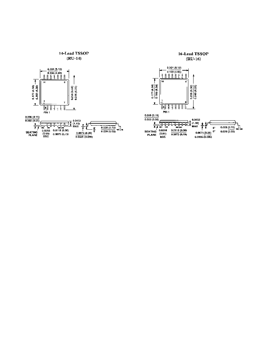
OUTLINE DIMENSIONS
Dimensions shown in inches and (mm)
Document Outline
- Specifications
- Pinout
- PAckage Drawings
- Ordering Guide
- Features
- Applications
- Product Description
- Timing characteristics
- Absolute Maximum Ratings
- Functional Block Diagram
- Pin Function Description
- AD5280 PIN CONFIGURATION
- AD5282 PIN CONFIGURATION
- DIAGRAMS
- Detail Timing Diagram
- Writing to the RDAC Register
- Reading Data from a Previously Selected RDAC Register
- AD5280/AD5282 Equivalent RDAC Circuit
- Level Shift for different potential operation.
- Multiple AD5282 Devices on One Bus
- ESD Protection of digital pins
- ESD Protection of Resistor Terminals
- Potentiometer Divider Nonlinearity error test circuit (INL, DNL)
- Resistor Position Nonlinearity Error (Rheostat Operation; R-INL, R-DNL)
- Wiper Resistance test Circuit
- Power supply sensitivity test circuit (PSS, PSSR)
- Inverting Gain test Circuit
- Non-Inverting Gain test circuit
- Gain Vs Frequency test circuit
- Incremental ON Resistance Test Circuit
- Common Mode Leakage current test circuit