 | ÐлекÑÑоннÑй компоненÑ: AD53020 | СкаÑаÑÑ:  PDF PDF  ZIP ZIP |
Äîêóìåíòàöèÿ è îïèñàíèÿ www.docs.chipfind.ru
REV. A
Information furnished by Analog Devices is believed to be accurate and
reliable. However, no responsibility is assumed by Analog Devices for its
use, nor for any infringements of patents or other rights of third parties
which may result from its use. No license is granted by implication or
otherwise under any patent or patent rights of Analog Devices.
a
AD53020
One Technology Way, P.O. Box 9106, Norwood, MA 02062-9106, U.S.A.
Tel: 781/329-4700
World Wide Web Site: http://www.analog.com
Fax: 781/326-8703
© Analog Devices, Inc., 1999
Four Channel ECL Delay Line
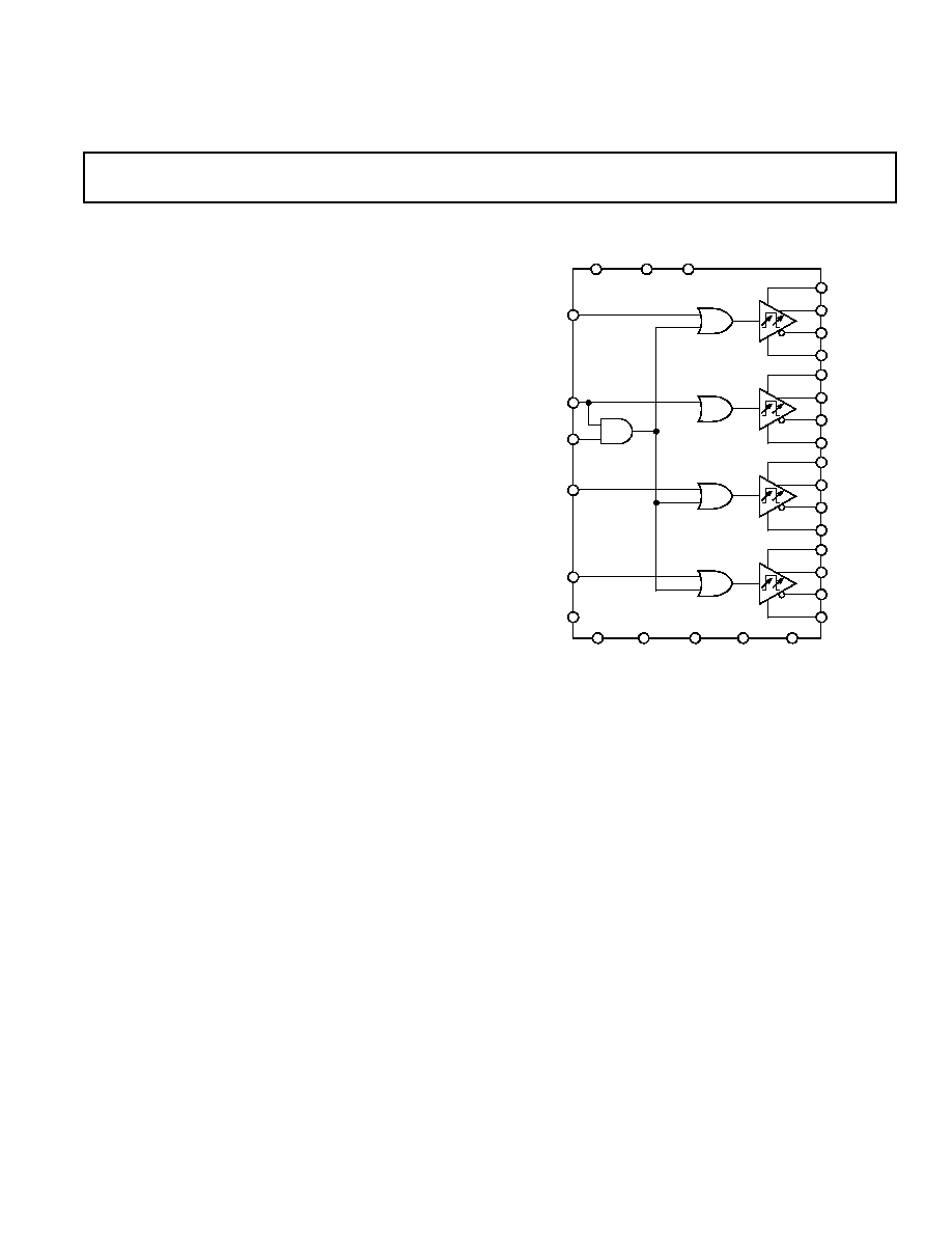
FUNCTIONAL BLOCK DIAGRAM
FEATURES
Four Delay Lines with the Ability to Independently
Adjust All Edges
Pin Compatible and Functionally Equivalent with the
BT624
Reduced Power Dissipation
44-Lead PLCC Package with Internal Heat Spreader
APPLICATIONS
Automatic Test Equipment
Semiconductor Test Systems
Board Test Systems
Clocked ECL Circuits
PRODUCT DESCRIPTION
The AD53020 is a four-channel delay line designed for use in
automatic test equipment and digital logic systems. High speed
bipolar transistors and a 44-lead plastic PLCC package with
internal heat spreader provide high frequency performance at a
minimum of space, cost and power dissipation.
Featuring full pin compatibility and functional equivalence to
the BT624, the AD53020 offers independent analog control of
positive and negative edges with five delay ranges. The AD53020
offers attractive performance with optimized power dissipation
and linear delay vs. program voltage control. This device is also
very stable over operating conditions and has very low jitter.
Digital inputs are ECL compatible. They can either be pro-
vided independently for each channel (IN1,
IN1 through IN4,
IN4), or fanned out to all channels from Channel 2 (IN2,
IN2). The choice of these two options is made by setting the
DRVMODE input, with ECL Logic 0 providing four indepen-
dent channels, and ECL Logic 1 enabling a logical OR function
between each channel and the Channel Number 2.
For maximum timing accuracy, differential signals are recom-
mended for use with the digital inputs. However, single-ended
operation is also supported and it is facilitated through the use
of the V
BB
midpoint level generated on-chip. To make use of
this feature, connect the V
BB
output to the inverting input of
each channel. It is also advisable, when using the V
BB
output,
to decouple this signal with a 0.1
µ
F ceramic capacitor to ground.
The outputs of the AD53020 are ECL compatible and should
be terminated by 50
to 2.0 V at the inputs of the gates
they drive.
The delay is programmed through the VDELAY and VWIDTH
pins for each channel. The acceptable range is 1.3 V to 0.1 V,
representing the longest and the shortest delays provided by the
device. An 0.01
µ
F ceramic capacitor to ground is recom-
mended for each input. The bias current for each input is fixed
by an internal current mirror. The value of the bias current is
set by the external resistor at REXT1. A 1.3 k
resistor to
ground at this pin establishes 1 mA bias in each input. The
nominal voltage at the REXT1 pin is 1.3 V.
The VDELAY affects both the positive and negative edges in all
modes. The VWIDTH is an additional delay adjustment that is
active in Modes 2, 3 and 5. VWIDTH has no effect in Modes 0
and 1. For Modes 2 and 3, the effect of the VWIDTH adjust-
ment is to increase or decrease the delay of the negative edge
relative to the positive edge. In Mode 5, the total delay for both
positive and negative edges is set by the combination of VDELAY
and VWIDTH.
(continued on page 4)
VWIDTH1
OUT1
OUT1
VDELAY1
VWIDTH2
VDELAY2
OUT2
OUT2
VWIDTH3
VWIDTH4
OUT3
OUT3
OUT4
OUT4
VDELAY4
VDELAY3
V
BB
COMP1
COMP2
REXT1
REXT2
V
EE
GND
S0
S1
IN1,
IN1
IN2,
IN2
IN3,
IN3
IN4,
IN4
DRVMODE
AD53020
2
REV. A
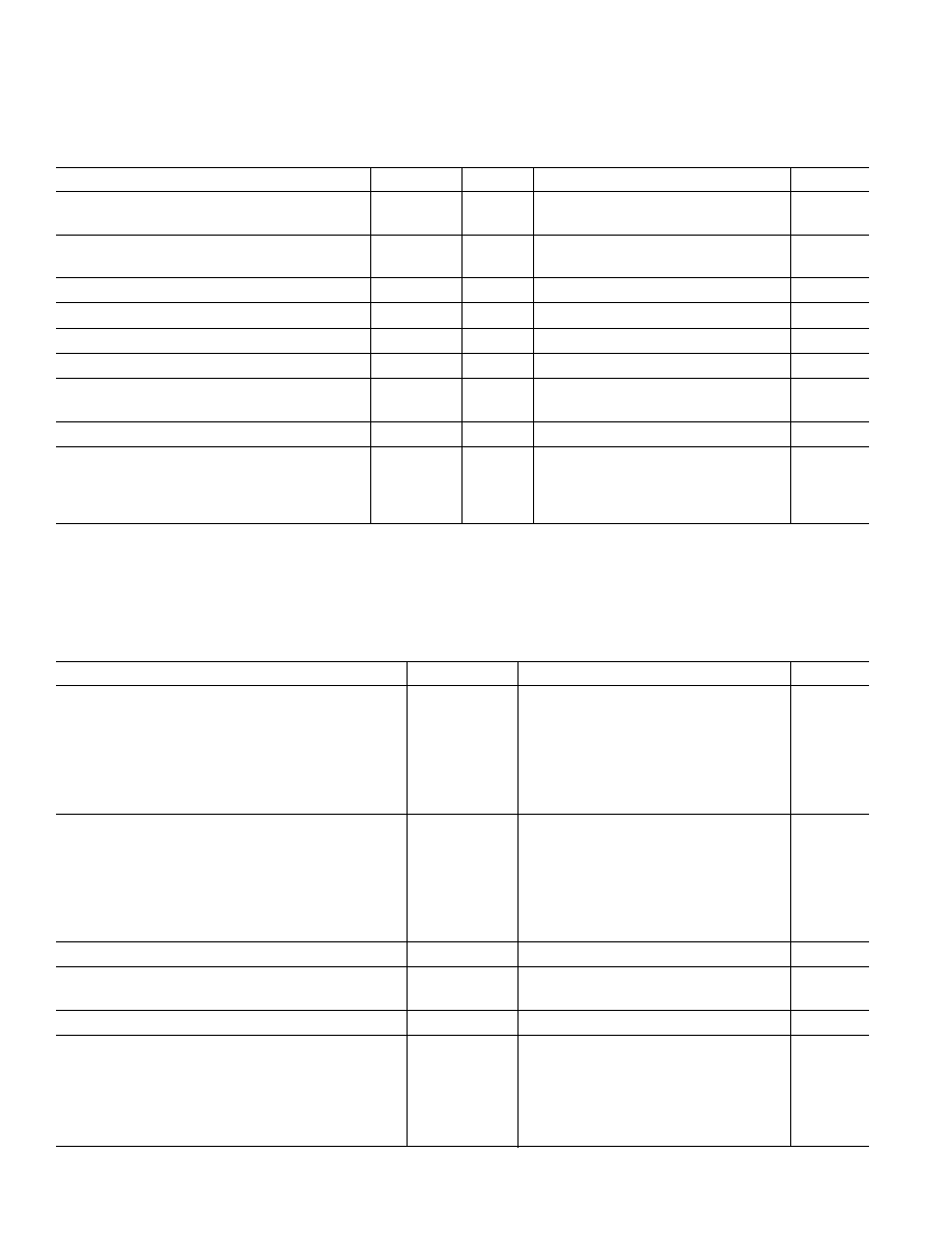
AD53020SPECIFICATIONS
DC CHARACTERISTICS
1
Parameter
Symbol
T( C)
Min
Typ
Max
Units
DIGITAL INPUT HIGH VOLTAGE
IN,
IN, DRVMODE, S0, S1
V
IH
70
1.070
0.000
V
DIGITAL INPUT LOW VOLTAGE
IN,
IN, DRVMODE, S0
V
IL
70
1.950
1.450
V
DIGITAL INPUT LOW VOLTAGE, S1
V
IL
70
V
EE
1.450
V
S1 THIRD STATE (EXTENDED DELAY)
Full
V
EE
3.2
V
DIGITAL OUTPUT HIGH VOLTAGE
V
OH
70
1.000
0.735
V
DIGITAL OUTPUT LOW VOLTAGE
V
OL
70
1.950
1.600
V
DIGITAL INPUT BIAS CURRENT
100 to
IN,
IN, DRVMODE, S0, S1
I
IN
+100
µ
A
POWER SUPPLY REJECTION RATIO
2
PSRR
Full
0.5
% Tpd/V
V
EE
SUPPLY CURRENT
Mode 0
I
EE
Full
174
200
mA
Modes 1, 2
I
EE
Full
225
250
mA
Modes 3, 5
I
EE
Full
267
290
mA
NOTES
1
The specified limits shown can be met only after thermal equilibrium has been established. Thermal equilibrium is established by applying power for at least two
minutes while maintaining a transverse air flow of 400 linear feet per minute over the device either mounted in the test socket or on the printed circuit board.
2
This parameter is fully characterized, but not production tested.
Specifications subject to change without notice.
AD53020-Test Conditions (Unless otherwise noted): Recommended Operating
Conditions with all OUT and
OUT outputs terminated through 50 to 2.0 V, REXT1 = 1.3 k , REXT2 = 2.94 k . Typical values are based on
nominal temperature, T
A
= +25 C, and nominal supply voltage, V
EE
= 5.2 V.
AC CHARACTERISTICS
1
Parameter
Symbol
Min
Typ
Max
Units
MINIMUM PROPAGATION DELAYS
2
Mode
S1
S0
VDELAY
0
0
0
0.1 V
Tpd Min
3.6
4.5
5.4
ns
1
0
1
0.1 V
Tpd Min
4.9
6.3
7.3
ns
2
1
0
0.1 V
Tpd Min
3.9
5.3
6.8
ns
3
1
1
0.1 V
Tpd Min
5.2
7.1
8.8
ns
5
V
EE
1
0.1 V
Tpd Min
6.8
8.8
10.3
ns
DELAY ADJUSTMENT RANGES
Mode
S1
S0
0
0
0
Tpd Span
14.0
19.0
24.7
ns
1
0
1
Tpd Span
22.9
31.4
37.8
ns
2
1
0
Tpd Span
13.2
18.9
24.6
ns
3
1
1
Tpd Span
22.0
31.5
40.6
ns
5
V
EE
1
Tpd Span
29.3
44.5
52.0
ns
MINIMUM PULSEWIDTH
3
1.9
ns
RISING EDGE DELAY VS. VWIDTH DELAY
Change (Modes 2 and 3)
3
30
ps
DELAY VS. DUTY CYCLE
3, 4
50
ps
VWIDTH RANGE OF ADJUSTMENT
(VDELAY = 0.6 V, MODES 2 AND 3, DELAY
RELATIVE TO VWIDTH = 0.7 V)
VWIDTH = 0.1 V
5.5
4.0
ns
VWIDTH = 1.1 V
+5.5
ns
VWIDTH = 1.3 V
+4.0
+6.5
ns
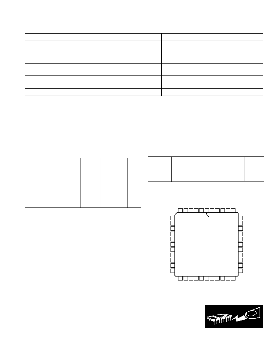
3
REV. A
AD53020
Parameter
Symbol
Min
Typ
Max
Units
RISING TO FALLING EDGE DELAY MATCHING
(VDELAY = VFALL = 0.5 V)
3
Modes
0, 1, 5
0.1
ns
Modes 2, 3
1.0
ns
PROPAGATION DELAY TEMPERATURE
COEFFICIENT
3, 5
0.05
% Tpd/
°
C
OUTPUT RISE/FALL TIMES
(20% to 80%)
3
550
ps
DELAY LINEARITY
3
MONOTONIC
NOTES
1
The specified limits shown can be met only after thermal equilibrium has been established. Thermal equilibrium is established by applying power for at least two
minutes while maintaining a transverse air flow of 400 linear feet per minute over the device either mounted in the test socket or on the printed circuit board.
2
All minimum propagation delay time measurements refer to both rising and falling edges for Modes 0, 1, 5; these measurements refer to rising edges for Modes 2 and
3 only. DRVMODE is logically low.
3
This parameter is fully characterized, but not production tested.
4
Delay on leading and trailing edges are measured by setting VDELAY = VWIDTH = 0.7 V. The variations for each delay are measured by changing the input duty
cycle from 5% to 95% at a constant frequency of 10 MHz.
5
Propagation delay temperature coefficient measured at VDELAY = VWIDTH = 0.7 V.
Specifications subject to change without notice.
ORDERING GUIDE
Package
Package
Model
Description
Option
AD53020
44-Lead Plastic Leaded Chip Carrier
P-44A
(PLCC)
ABSOLUTE MAXIMUM RATINGS
1
Parameter
Symbol
Min
Max
Units
V
EE
(Relative to GND)
6.0
0
V
Voltage on Any Digital Pin
V
EE
V
Output Current
50
mA
Ambient Operating Temperature
T
A
55
+70
°
C
Storage Temperature
T
S
65
+150
°
C
Junction Temperature
T
J
+150
°
C
Soldering Temperature
2
(Soldering, 5 sec)
T
SOL
+260
°
C
NOTES
1
Stresses above those listed under Absolute Maximum Ratings may cause perma-
nent damage to the device. This is a stress rating only; functional operation of the
device at these or any other conditions above those listed in the operational sections
of this specification is not implied. Absolute maximum limits apply individually,
not in combination. Exposure to absolute maximum rating conditions for ex-
tended periods of time may affect device reliability.
2
To ensure lead solderability, handling with bare hands should be avoided and the
device should be stored in environments at 24
°
C
±
5
°
C (75
°
F
±
10
°
F) with relative
humidity not to exceed 65%.
CAUTION
ESD (electrostatic discharge) sensitive device. Electrostatic charges as high as 4000 V readily
accumulate on the human body and test equipment and can discharge without detection.
Although the AD53020 features proprietary ESD protection circuitry, permanent damage may
occur on devices subjected to high energy electrostatic discharges. Therefore, proper ESD
precautions are recommended to avoid performance degradation or loss of functionality.
WARNING!
ESD SENSITIVE DEVICE
PIN CONFIGURATION
9
10
11
12
13
7
8
16
17
14
15
2
1
44
3
4
5
6
42 41 40
43
35
36
37
38
39
33
34
31
32
29
30
IN1
IN1
GND1
COMP1
REXT1
COMP2
REXT2
GND3
GND4
OUT3
OUT3
OUT2
IN4
V
EE4
VDELAY4
VWIDTH4
VDELAY3
VWIDTH3
VDELAY2
VWIDTH2
VDELAY1
VWIDTH1
V
BB
DRVMODE
S0
S1
GND1
IN4
GND4
V
EE3
IN3
IN3
GND3
V
EE2
IN2
IN2
GND2
V
EE1
18 19 20 21 22 23 24 25 26 27 28
PIN 1
IDENTIFIER
TOP VIEW
(Not to Scale)
AD53020
OUT2
GND2
OUT1
OUT1
OUT4
OUT4
AD53020
4
REV. A
C3265a02/99
PRINTED IN U.S.A.
A second bias current reference is employed to set the bias
current of the delay cells. This current is set by the external
resistor at REXT2. A 2.94 k
resistor sets the nominal bias
current of 500
µ
A. The nominal voltage at the REXT2 pin
is 1.47 V.
The current references require compensation capacitors of
0.1
µ
F to V
EE
at each of the COMP1 and COMP2 pins. In
addition, each V
EE
supply pin should also have its own decou-
pling capacitor of 0.1
µ
F to ground.
All decoupling capacitors should be located as close as possible
to the AD53020 chip.
The mode is set by the inputs S0 and S1. These pins use stan-
dard ECL levels, with the addition of a third level for the S1
Pin, which can also be connected to V
EE
. Refer to Table I for
the description of the modes and their respective settings.
For Modes 2 and 3, it is important to note that an internal flip-
flop is used to provide the independent control of rising and
falling edges. The state of this flip-flop is indeterminate upon
power-up. The state becomes fixed once the first full pulse is
provided to each channel, consisting of a positive edge followed
by a negative edge.
Table I. Truth Table for Mode Determination
Typical Independent Adjustment of
S1
S0
Mode
Span
Positive and Negative Edges?
0
0
0
19 ns
No
0
1
1
31 ns
No
1
0
2
19 ns
Yes
1
1
3
31 ns
Yes
V
EE
0
Not Valid
V
EE
1
5
45 ns
No
S0 and S1 accept logical ECL levels. In the case of S1 only, a third state is also
accepted, at the negative supply, V
EE
.
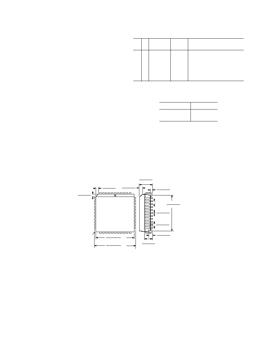
Table II. Package Thermal Characteristics
Air Flow, FM
JA
, C/W
0
30.2
400
20.9
6
PIN 1
IDENTIFIER
7
40
39
17
18
29
28
TOP VIEW
(PINS DOWN)
0.695 (17.65)
0.685 (17.40)
SQ
0.656 (16.66)
0.650 (16.51)
SQ
0.048 (1.21)
0.042 (1.07)
0.048 (1.21)
0.042 (1.07)
0.020
(0.50)
R
0.021 (0.53)
0.013 (0.33)
0.050
(1.27)
BSC
0.63 (16.00)
0.59 (14.99)
0.032 (0.81)
0.026 (0.66)
0.180 (4.57)
0.165 (4.19)
0.040 (1.01)
0.025 (0.64)
0.025 (0.63)
0.015 (0.38)
0.110 (2.79)
0.085 (2.16)
0.056 (1.42)
0.042 (1.07)
44-Lead PLCC
(P-44A)
OUTLINE DIMENSIONS
Dimensions shown in inches and (mm).