
REV. A
Information furnished by Analog Devices is believed to be accurate and
reliable. However, no responsibility is assumed by Analog Devices for its
use, nor for any infringements of patents or other rights of third parties
which may result from its use. No license is granted by implication or
otherwise under any patent or patent rights of Analog Devices.
a
AD53042
One Technology Way, P.O. Box 9106, Norwood, MA 02062-9106, U.S.A.
Tel: 781/329-4700
World Wide Web Site: http://www.analog.com
Fax: 781/326-8703
© Analog Devices, Inc., 1999
High Speed Window Comparator
FUNCTIONAL BLOCK DIAGRAM
LATCH/OUTPUT
A
LEA
LEA NC +V
S
NC GND
AD53042
LEB
LEB NC
≠V
S
NC
GND
GND
GND
GND
V
A
NC
V
IN
NC
V
B
GND
GND
QA
QA
DGND
QB
QB
GND
NOTE:
NOT THE ACTUAL PHYSICAL LAYOUT OF DEVICE.
NC = NO CONNECTION INSIDE PACKAGE.
LATCH/OUTPUT
B
FEATURES
≠2 V to +7 V Input Voltage Range
Low V
IN
Bias Current (<100 nA)
Up to 5 V/ns Input Signal Tracking
Low Dispersion of 100 ps
28-Lead PLCC Package
APPLICATIONS
Automatic Test Equipment
Semiconductor Test Systems
Board Test Systems
PRODUCT DESCRIPTION
The AD53042 is an ultrahigh speed window comparator
with latch. It uses a high speed monolithic process to provide
high dc accuracy without sacrificing input voltage range.
On-chip connection of the common input eliminates the
contributions of a second bonding pad and package pin to
the input capacitance, resulting in a maximum input
capacitance of 2 pF.
The AD53042 employs a high precision differential input
stage with a common mode range of 9 V. Its complementary
digital outputs are fully ECL-compatible. The output stage is
capable of driving a 50
line terminated to ≠2 V. The device
also provides a latch function, allowing operation in track-hold
mode and can also be used to generate hysteresis.
2.8V
0.2V
3.0V
0V
0V
3.0V
MIN. POSITIVE
INPUT PULSE
MIN. NEGATIVE
INPUT PULSE
Figure 1. Typical Application Circuit

≠ 2 ≠
REV. A
AD53042≠SPECIFICATIONS
(All specifications apply with T
C
= 40 C to 100 C and +V
S
= +7.75 V to +11.5 V;
≠V
S
= ≠3.95 V to ≠7.7 V unless otherwise noted.)
Parameter
Min
Typ
Max
Units
Test Conditions
POWER SUPPLIES
Positive Supply Currents
65
mA
No Load
Negative Supply Current
≠85
mA
No Load
Power Dissipation
1.19
W
No Load, +V
S
= +10 V, ≠V
S
= ≠5.2 V
DC INPUT CHARACTERISTICS
Offset Voltage (V
OS
)
≠10
10
mV
CMV = 0 V
V
IN
Bias Current
≠0.5
<0.1
0.5
µ
A
V
IN
= 0 V
V
A
, V
B
Bias Current
≠20
20
µ
A
V
IN
= 0 V
Capacitance V
IN
, V
A
, V
B
2
pF
Voltage Range (V
CM
)
≠V
S
+ 2.7
+V
S
≠ 2.5
V
Differential Voltage (V
DIFF
)
9
V
Nonlinearity
≠5
5
mV
See Note 1
V
A
/V
B
Interaction
0.1
mV/V
BIAS CURRENT
Change vs. Comparator State
≠1
1
µ
A
Nonlinearity
≠2
2
µ
A
Tempco
±
0.1
µ
A/
∞
C
LATCH ENABLE INPUTS
Common-Mode Range
≠2
1
V
Differential Voltage
0.4
3
V
Logic "1" Current (L
IH
)
200
µ
A
Logic "0" Current (L
IL
)
≠10
µ
A
DIGITAL OUTPUTS
Logic "1" Voltage (V
OH
)
≠0.98
V
Q or
Q, 50
to ≠2 V
Logic "0" Voltage (V
OL
)
≠1.5
V
Q or
Q, 50
to ≠2 V
SWITCHING PERFORMANCE
Propagation Delay
Input to Output
2
ns
V
IN
= 2 V p-p, t
PDR
, t
PDF
, Figure 1, Note 2
Latch Enable to Output
1.2
ns
Part-to-Part Skew
1
ns
Change vs. Temperature
±
1
ps/
∞
C
DISPERSION
5 V p-p Input (All Edges)
±
100
ps
10%, 90% 0.5 V/ns, 3 V/ns
5 V p-p Input (All Edges)
±
175
ps
10%, 90% 5 V/ns
V Slew = 1 V/ns (All Edges)
±
50
ps
10%, 90% 3 V, 5 V
V Slew = 1 V/ns (All Edges)
±
50
ps
20%, 80% 1 V
Minimum Pulsewidth
<1
ns
See Note 3
Edge Interaction
<200
ps
See Note 4
Duty Ratio
<100
ps
See Note 5
Comparator Interaction
<100
ps
NOTES
1
Defined as change in V
OS
from ≠V
S
+ 2.95 V to +V
S
≠ 2.75 V (throughout the range) after V
A
and V
B
are corrected for gain and offset using 0 V and 5 V.
2
Propagation delay is measured from the input threshold crossing at the 50% point of a 0 V to 5 V input to the output Q and
Q crossing.
3
The minimum input pulsewidth that will maintain a 600 mV ECL swing on the output. The input is a 0 V to 3 V signal with a 3 V/ns rise and fall times. The input
pulsewidth is measured between the 2.8 V point of a positive input pulse and the 0.2 V of a negative input pulse. See Figure 2.
4
Maximum Change in propagation delay as the input pulse is reduced from 50 ns to a 2 ns pulsewidth. 0 V to 3 V swing with 3 V/ns rise/fall time and 25% duty cycle.
5
Maximum Change in propagation delay as the input pulse is reduced from 99% to a 1% duty cycle. 0 V to 3 V swing with 3 V/ns rise/fall time and 50 ns to 4.95
µ
s
pulsewidth, period = 5
µ
s.
Specifications subject to change without notice.
AD53042
≠ 3 ≠
REV. A
CAUTION
ESD (electrostatic discharge) sensitive device. Electrostatic charges as high as 4000 V readily
accumulate on the human body and test equipment and can discharge without detection.
Although the AD53042 features proprietary ESD protection circuitry, permanent damage may
occur on devices subjected to high energy electrostatic discharges. Therefore, proper ESD
precautions are recommended to avoid performance degradation or loss of functionality.
ABSOLUTE MAXIMUM RATINGS*
Power Supply Voltage
+V
S
to GND . . . . . . . . . . . . . . . . . . . . . . . . . . . . . . . +12 V
≠V
S
to GND . . . . . . . . . . . . . . . . . . . . . . . . . . . . . . . . . ≠8 V
+V
S
to ≠V
S
. . . . . . . . . . . . . . . . . . . . . . . . . . . . . . . . . +17 V
Inputs
V
IN
, V
A
, V
B
. . . . . . . . . . . . . . . +V
S
≠ 13.5 V, ≠V
S
+ 13.7 V
LEA,
LEA, LEB, LEB . . . . . . . . . +V
S
≠ 14 V, ≠V
S
+10 V
Currents
+V
S
. . . . . . . . . . . . . . . . . . . . . . . . . . . . . . . . . . . . . 95 mA
≠V
S
. . . . . . . . . . . . . . . . . . . . . . . . . . . . . . . . . . . . . . ≠75 mA
QA,
QA, QB, QB . . . . . . . . . . . . . . . . . . ≠40 mA to +2 mA
Environmental
Operating Temperature (Ambient) . . . . . . . . 0
∞
C to +70
∞
C
Storage Temperature . . . . . . . . . . . . . . . . ≠65
∞
C to +125
∞
C
Lead Temperature (Soldering, 20 sec) . . . . . . . . . . . +300
∞
C
*Stresses above those listed under Absolute Maximum Ratings may cause perma-
nent damage to the device. This is a stress rating only; functional operation of the
device at these or any other conditions above those indicated in the operational
sections of this specification is not implied. Absolute maximum limits apply
individually, not in combination. Exposure to absolute maximum rating condi-
tions for extended periods may affect device reliability.
The device must suffer no reliability degradation if any supply pin is either shorted
to ground or left floating for an indefinite periods of time during normal operation.
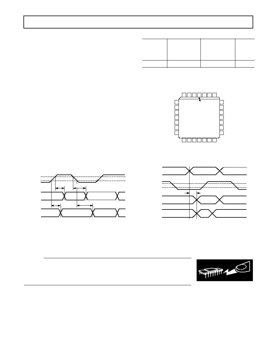
PIN CONFIGURATION
7
8
9
10
11
5
6
28 27 26
1
2
3
4
12 13
14 15 16 17 18
TOP VIEW
(Not to Scale)
PIN 1
IDENTIFIER
21
22
23
24
25
19
20
GND
VINA
NC
VINAB
NC
GND
QA
QA
DGND
QB
NC = NO CONNECT
AD53042
VINB
GND
QB
GND
VNEG
GND
LEB
LEB
NC
NC
GND
GND
LEA
NC
VPOS
LEA
NC
GND
ORDERING GUIDE
Shipment Method,
Quantity
Package
Per Shipping
Package
Model
Description
Container
Option
AD53042KRP
28-Lead PLCC
Tube, 36 Pieces
P-28A
WARNING!
ESD SENSITIVE DEVICE
V
A
V
B
V
IN
QA
QA
QB
QB
LEA, LEB
LEA
,
LEB
~
1.2ns
Figure 3. Timing Diagram II
If either of the latch enables, LEA or LEB are low, the output
follows the input. If LEA or LEB are high, the comparator out-
puts will be latched and they won't change.
V
A
V
B
V
IN
QA
QA
QB
QB
t
PDR
t
PDF
t
PDR
t
PDF
Figure 2. Timing Diagram I
AD53042
≠ 4 ≠
REV. A
C3120a≠0≠5/99
PRINTED IN U.S.A.
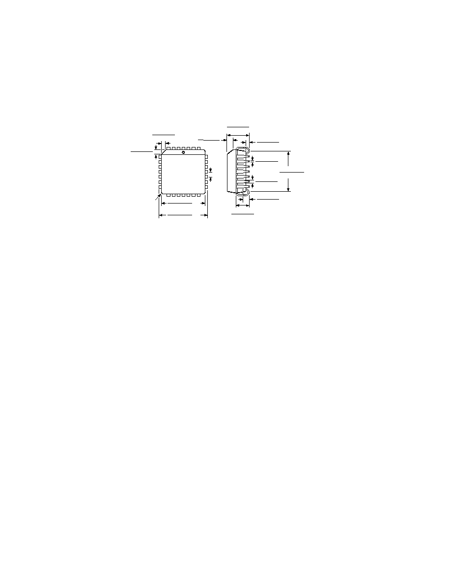
OUTLINE DIMENSIONS
Dimensions shown in inches and (mm).
28-Lead Plastic Leaded Chip Carrier
(P-28A)
4
PIN 1
IDENTIFIER
5
26
25
11
12
19
18
TOP VIEW
(PINS DOWN)
0.495 (12.57)
0.485 (12.32)
SQ
0.456 (11.58)
0.450 (11.43)
SQ
0.048 (1.21)
0.042 (1.07)
0.048 (1.21)
0.042 (1.07)
0.020
(0.50)
MAX
(3) PLACES
0.050
(1.27)
BSC
0.021 (0.53)
0.013 (0.33)
0.430 (10.92)
0.390 (9.91)
0.032 (0.81)
0.026 (0.66)
0.180 (4.57)
0.165 (4.19)
0.040 (1.01)
0.025 (0.64)
0.056 (1.42)
0.042 (1.07)
0.025 (0.63)
0.015 (0.38)
0.110 (2.79)
0.085 (2.16)