 | ÐлекÑÑоннÑй компоненÑ: AD5313B | СкаÑаÑÑ:  PDF PDF  ZIP ZIP |
AD5303/13/23 Data Sheet
REV. 0
Information furnished by Analog Devices is believed to be accurate and
reliable. However, no responsibility is assumed by Analog Devices for its
use, nor for any infringements of patents or other rights of third parties
which may result from its use. No license is granted by implication or
otherwise under any patent or patent rights of Analog Devices.
a
AD5303/AD5313/AD5323*
One Technology Way, P.O. Box 9106, Norwood, MA 02062-9106, U.S.A.
Tel: 781/329-4700
World Wide Web Site: http://www.analog.com
Fax: 781/326-8703
© Analog Devices, Inc., 1999
+2.5 V to +5.5 V, 230 A, Dual Rail-to-Rail
Voltage Output 8-/10-/12-Bit DACs
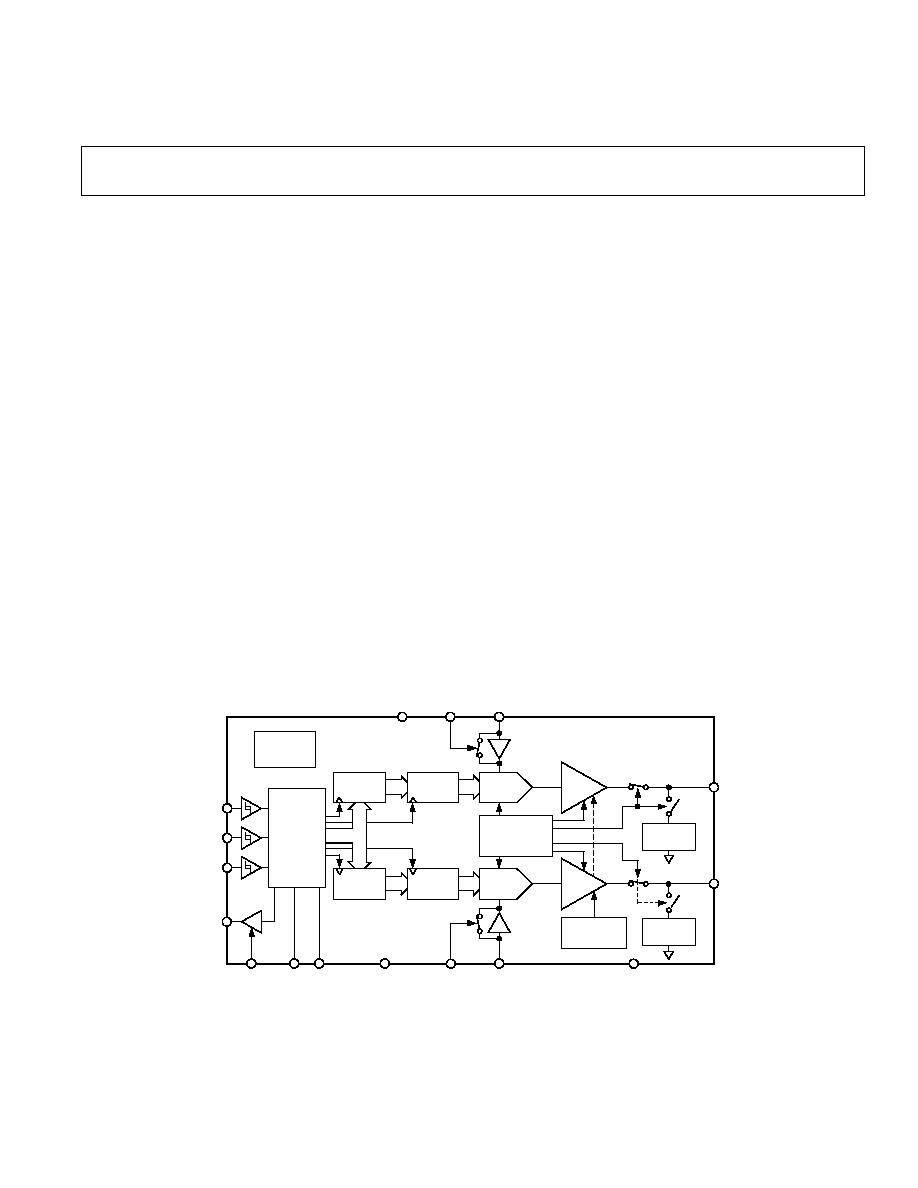
FUNCTIONAL BLOCK DIAGRAM
BUFFER
POWER-DOWN
LOGIC
RESISTOR
NETWORK
STRING
DAC
AD5303/AD5313/AD5323
V
OUT
A
V
OUT
B
V
DD
V
REF
A
V
REF
B
DAC
REGISTER
DAC
REGISTER
>
SYNC
SCLK
DIN
GND
BUF A
SDO
CLR
BUF B
STRING
DAC
DCEN
LDAC
POWER-ON
RESET
PD
BUFFER
GAIN-SELECT
LOGIC
RESISTOR
NETWORK
INPUT
REGISTER
INPUT
REGISTER
INTERFACE
LOGIC
FEATURES
AD5303: Two Buffered 8-Bit DACs in One Package
AD5313: Two Buffered 10-Bit DACs in One Package
AD5323: Two Buffered 12-Bit DACs in One Package
16-Lead TSSOP Package
Micropower Operation: 300 A @ 5 V (Including
Reference Current)
Power-Down to 200 nA @ 5 V, 50 nA @ 3 V
+2.5 V to +5.5 V Power Supply
Double-Buffered Input Logic
Guaranteed Monotonic By Design Over All Codes
Buffered/Unbuffered Reference Input Options
Output Range: 0V
REF
or 02 V
REF
Power-On-Reset to Zero Volts
SDO Daisy-Chaining Option
Simultaneous Update of DAC Outputs via LDAC Pin
Asynchronous CLR Facility
Low Power Serial Interface with Schmitt-Triggered
Inputs
On-Chip Rail-to-Rail Output Buffer Amplifiers
APPLICATIONS
Portable Battery Powered Instruments
Digital Gain and Offset Adjustment
Programmable Voltage and Current Sources
Programmable Attenuators
GENERAL DESCRIPTION
The AD5303/AD5313/AD5323 are dual 8-, 10- and 12-bit
buffered voltage output DACs in a 16-lead TSSOP package that
operate from a single +2.5 V to +5.5 V supply consuming 230
µA
at 3 V. Their on-chip output amplifiers allow the outputs to
swing rail-to-rail with a slew rate of 0.7 V/
µs. The AD5303/
AD5313/AD5323 utilize a versatile 3-wire serial interface that
operates at clock rates up to 30 MHz and is compatible with
standard SPITM, QSPI, MICROWIRETM and DSP interface
standards.
The references for the two DACs are derived from two reference
pins (one per DAC). These reference inputs may be configured
as buffered or unbuffered inputs. The parts incorporate a power-
on-reset circuit that ensures that the DAC outputs power-up to
0 V and remain there until a valid write to the device takes place.
There is also an asynchronous active low CLR pin that clears
both DACs to 0 V. The outputs of both DACs may be updated
simultaneously using the asynchronous LDAC input. The
parts contain a power-down feature that reduces the current
consumption of the devices to 200 nA at 5 V (50 nA at 3 V) and
provides software-selectable output loads while in power-down
mode. The parts may also be used in daisy-chaining applications
using the SDO pin.
The low power consumption of these parts in normal operation
make them ideally suited to portable battery operated equip-
ment. The power consumption is 1.5 mW at 5 V, 0.7 mW at
3 V, reducing to 1
µW in power-down mode.
*Protected by U.S. Patent No. 5684481; other patents pending.
SPI is a trademark of Motorola, Inc.
MICROWIRE is a trademark of National Semiconductor Corporation.

REV. 0
2
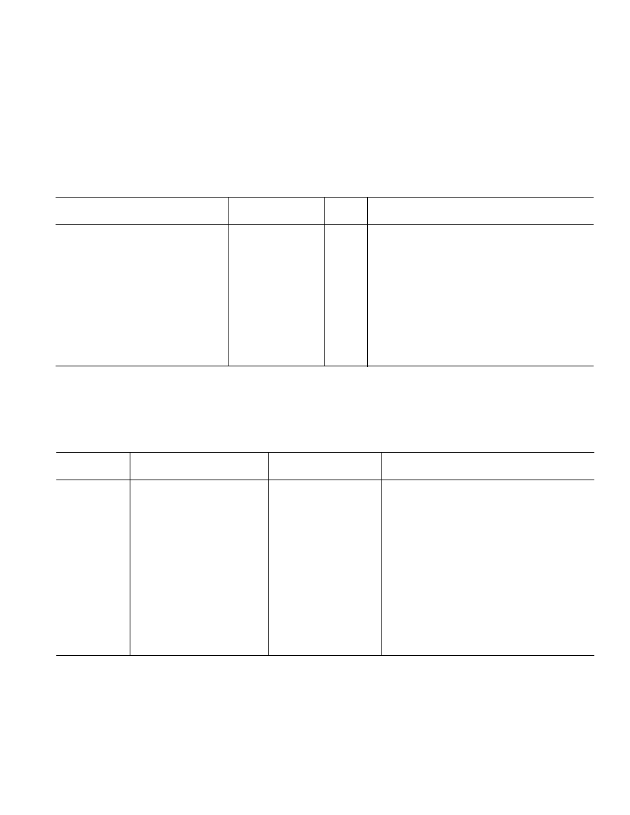
AD5303/AD5313/AD5323SPECIFICATIONS
(V
DD
= +2.5 V to +5.5 V; V
REF
= +2 V; R
L
= 2 k to GND; C
L
= 200 pF to GND; all specifications T
MIN
to T
MAX
unless otherwise noted.)
B Version
2
Parameter
1
Min
Typ
Max
Units
Conditions/Comments
DC PERFORMANCE
3, 4
AD5303
Resolution
8
Bits
Relative Accuracy
±0.15
±1
LSB
Differential Nonlinearity
±0.02
±0.25
LSB
Guaranteed Monotonic by Design Over All Codes
AD5313
Resolution
10
Bits
Relative Accuracy
±0.5
±3
LSB
Differential Nonlinearity
±0.05
±0.5
LSB
Guaranteed Monotonic by Design Over All Codes
AD5323
Resolution
12
Bits
Relative Accuracy
±2
±12
LSB
Differential Nonlinearity
±0.2
±1
LSB
Guaranteed Monotonic by Design Over All Codes
Offset Error
±0.4
±3
% of FSR
See Figures 3 and 4
Gain Error
±0.15
±1
% of FSR
See Figures 3 and 4
Lower Deadband
10
60
mV
See Figures 3 and 4
Offset Error Drift
5
12
ppm of FSR/
°C
Gain Error Drift
5
5
ppm of FSR/
°C
Power Supply Rejection Ratio
5
60
dB
V
DD
=
±10%
DC Crosstalk
5
30
µV
DAC REFERENCE INPUTS
5
V
REF
Input Range
1
V
DD
V
Buffered Reference Mode
0
V
DD
V
Unbuffered Reference Mode
V
REF
Input Impedance
>10
M
Buffered Reference Mode
180
k
Unbuffered Reference Mode. 0V
REF
Output Range,
Input Impedance = R
DAC
90
k
Unbuffered Reference Mode. 02 V
REF
Output Range,
Input Impedance = R
DAC
Reference Feedthrough
90
dB
Frequency = 10 kHz
Channel-to-Channel Isolation
80
dB
Frequency = 10 kHz
OUTPUT CHARACTERISTICS
5
Minimum Output Voltage
6
0.001
V mi
n
This is a measure of the minimum and maximum
Maximum Output Voltage
6
V
DD
0.001
V max
drive capability of the output amplifier.
DC Output Impedance
0.5
Short Circuit Current
50
mA
V
DD
= +5 V
20
mA
V
DD
= +3 V
Power-Up Time
2.5
µs
Coming Out of Power-Down Mode. V
DD
= +5 V
5
µs
Coming Out of Power-Down Mode. V
DD
= +3 V
LOGIC INPUTS
5
Input Current
±1
µA
V
IL
, Input Low Voltage
0.8
V
V
DD
= +5 V
± 10%
0.6
V
V
DD
= +3 V
± 10%
0.5
V
V
DD
= +2.5 V
V
IH
, Input High Voltage
2.4
V
V
DD
= +5 V
± 10%
2.1
V
V
DD
= +3 V
± 10%
2.0
V
V
DD
= +2.5 V
Pin Capacitance
2
3.5
pF
LOGIC OUTPUT (SDO)
5
V
DD
= +5 V
± 10%
Output Low Voltage
0.4
V
I
SINK
= 2 mA
Output High Voltage
4.0
V
I
SOURCE
= 2 mA
V
DD
= +3 V
± 10%
Output Low Voltage
0.4
V
I
SINK
= 2 mA
Output High Voltage
2.4
V
I
SOURCE
= 2 mA
Floating-State Leakage Current
1
µA
DCEN = GND
Floating State O/P Capacitance
3
pF
DCEN = GND
POWER REQUIREMENTS
V
DD
2.5
5.5
V
I
DD
Specification Is Valid for All DAC Codes
I
DD
(Normal Mode)
Both DACs Active and Excluding Load Currents
V
DD
= +4.5 V to +5.5 V
300
450
µA
Both DACs in Unbuffered Mode. V
IH
= V
DD
and
V
DD
= +2.5 V to +3.6 V
230
350
µA
V
IL
= GND. In Buffered Mode, extra current is
typically x
µA per DAC where x = 5 µA + V
REF
/R
DAC
.
I
DD
(Full Power-Down)
V
DD
= +4.5 V to +5.5 V
0.2
1
µA
V
DD
= +2.5 V to +3.6 V
0.05
1
µA
REV. 0
AD5303/AD5313/AD5323
3
AC CHARACTERISTICS
1
(V
DD
= +2.5 V to +5.5 V; R
L
= 2 k to GND; C
L
= 200 pF to GND; all specifications T
MIN
to T
MAX
unless
otherwise noted.)
B Version
3
Parameter
2
Min
Typ
Max
Units
Conditions/Comments
Output Voltage Settling Time
V
REF
= V
DD
= +5 V
AD5303
6
8
µs
1/4 Scale to 3/4 Scale
Change
(40 Hex to C0 Hex)
AD5313
7
9
µs
1/4 Scale to 3/4 Scale
Change
(100 Hex to 300 Hex)
AD5323
8
10
µs
1/4 Scale to 3/4 Scale
Change
(400 Hex to C00 Hex)
Slew Rate
0.7
V/
µs
Major-Code Transition Glitch Energy
12
nV-s
1 LSB Change Around Major Carry
(011 . . . 11 to 100 . . . 00)
Digital Feedthrough
0.10
nV-s
Analog Crosstalk
0.01
nV-s
DAC-to-DAC Crosstalk
0.01
nV-s
Multiplying Bandwidth
200
kHz
V
REF
= 2 V
± 0.1 V p-p. Unbuffered Mode
Total Harmonic Distortion
70
dB
V
REF
= 2.5 V
± 0.1 V p-p. Frequency = 10 kHz
NOTES
1
Guaranteed by design and characterization, not production tested.
2
See Terminology.
3
Temperature range: B Version: 40
°C to +105°C.
Specifications subject to change without notice.
TIMING CHARACTERISTICS
1, 2, 3
Limit at T
MIN
, T
MAX
Parameter
(B Version)
Units
Conditions/Comments
t
1
33
ns min
SCLK Cycle Time
t
2
13
ns min
SCLK High Time
t
3
13
ns min
SCLK Low Time
t
4
0
ns min
SYNC to SCLK Rising Edge Setup Time
t
5
5
ns min
Data Setup Time
t
6
4.5
ns min
Data Hold Time
t
7
0
ns min
SCLK Falling Edge to SYNC Rising Edge
t
8
100
ns min
Minimum SYNC High Time
t
9
20
ns min
LDAC Pulsewidth
t
10
20
ns min
SCLK Falling Edge to LDAC Rising Edge
t
11
20
ns min
CLR Pulsewidth
t
12
4, 5
5
ns min
SCLK Falling Edge to SDO Invalid
t
13
4, 5
20
ns max
SCLK Falling Edge to SDO Valid
t
14
5
0
ns min
SCLK Falling Edge to SYNC Rising Edge
t
15
5
10
ns min
SYNC Rising Edge to SCLK Rising Edge
NOTES
1
Guaranteed by design and characterization, not production tested.
2
All input signals are specified with tr = tf = 5 ns (10% to 90% of V
DD
) and timed from a voltage level of (V
IL
+ V
IH
)/2.
3
See Figures 1 and 2.
4
These are measured with the load circuit of Figure 1.
5
Daisy-Chain Mode only (see Figure 45).
Specifications subject to change without notice.
(V
DD
= +2.5 V to +5.5 V; all specifications T
MIN
to T
MAX
unless otherwise noted.)
NOTES
1
See Terminology.
2
Temperature range: B Version: 40
°C to +105°C.
3
DC specifications tested with the outputs unloaded.
4
Linearity is tested using a reduced code range: AD5303 (Code 8 to 248); AD5313 (Code 28 to 995); AD5323 (Code 115 to 3981).
5
Guaranteed by design and characterization, not production tested.
6
In order for the amplifier output to reach its minimum voltage, Offset Error must be negative. In order for the amplifier output to reach its maximum voltage, V
REF
=
V
DD
and "Offset plus Gain" Error must be positive.
Specifications subject to change without notice.
REV. 0
AD5303/AD5313/AD5323
4
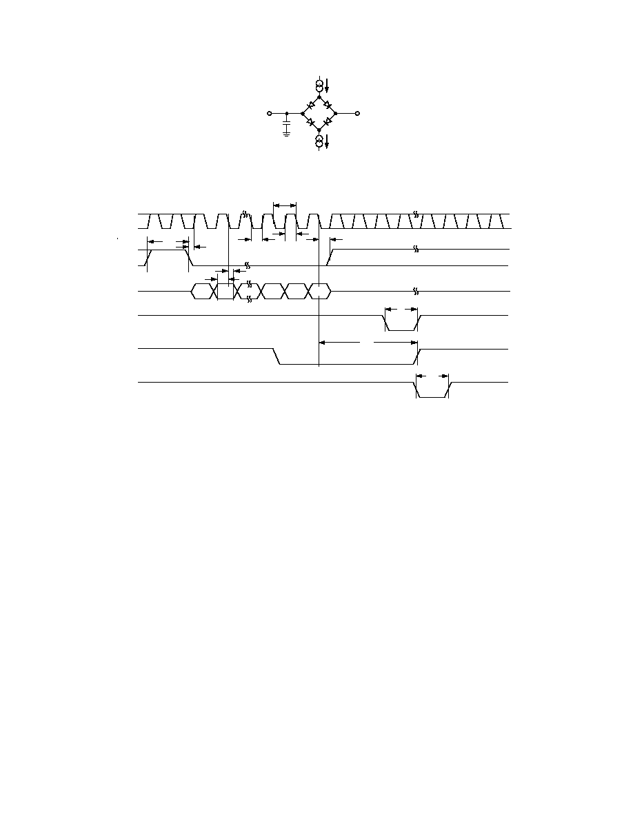
I
OL
2mA
I
OH
2mA
C
L
50pF
TO
OUTPUT
PIN
+1.6V
Figure 1. Load Circuit for Digital Output (SDO) Timing Specifications
SCLK
SYNC
DIN*
t
2
t
3
t
5
t
6
t
7
t
4
DB15
t
1
DB0
t
9
t
10
t
11
LDAC
LDAC
CLR
*SEE PAGE 12 FOR DESCRIPTION OF INPUT REGISTER
t
8
Figure 2. Serial Interface Timing Diagram
REV. 0
AD5303/AD5313/AD5323
5
CAUTION
ESD (electrostatic discharge) sensitive device. Electrostatic charges as high as 4000 V readily
accumulate on the human body and test equipment and can discharge without detection.
Although the AD5303/AD5313/AD5323 features proprietary ESD protection circuitry, perma-
nent damage may occur on devices subjected to high energy electrostatic discharges. Therefore,
proper ESD precautions are recommended to avoid performance degradation or loss of functionality.
WARNING!
ESD SENSITIVE DEVICE
ABSOLUTE MAXIMUM RATINGS
1, 2
(T
A
= +25
°C unless otherwise noted)
V
DD
to GND . . . . . . . . . . . . . . . . . . . . . . . . . . 0.3 V to +7 V
Digital Input Voltage to GND . . . . . . . 0.3 V to V
DD
+ 0.3 V
Digital Output Voltage to GND . . . . . 0.3 V to V
DD
+ 0.3 V
Reference Input Voltage to GND . . . . 0.3 V to V
DD
+ 0.3 V
V
OUT
A, V
OUT
B to GND . . . . . . . . . . . 0.3 V to V
DD
+ 0.3 V
Operating Temperature Range
Industrial (B Version) . . . . . . . . . . . . . . . 40
°C to +105°C
Storage Temperature Range . . . . . . . . . . . . 65
°C to +150°C
Junction Temperature (T
J
Max) . . . . . . . . . . . . . . . . . +150
°C
16-Lead TSSOP Package
Power Dissipation . . . . . . . . . . . . . . . . . . (T
J
Max T
A
)/
JA
JA
Thermal Impedance . . . . . . . . . . . . . . . . . . . . 160
°C/W
Lead Temperature, Soldering
Vapor Phase (60 sec) . . . . . . . . . . . . . . . . . . . . . . +215
°C
Infrared (15 sec) . . . . . . . . . . . . . . . . . . . . . . . . . . +220
°C
NOTES
1
Stresses above those listed under Absolute Maximum Ratings may cause perma-
nent damage to the device. This is a stress rating only; functional operation of the
device at these or any other conditions above those listed in the operational
sections of this specification is not implied. Exposure to absolute maximum rating
conditions for extended periods may affect device reliability.
2
Transient currents of up to 100 mA will not cause SCR latch-up.
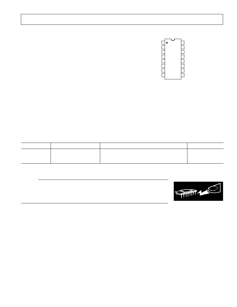
PIN CONFIGURATION
TOP VIEW
(Not to Scale)
16
15
14
13
12
11
10
9
1
2
3
4
5
6
7
8
CLR
LDAC
V
DD
V
REF
B
V
REF
A
V
OUT
A
BUF A
BUF B
SDO
GND
DIN
SCLK
SYNC
V
OUT
B
PD
DCEN
AD5303/
AD5313/
AD5323
ORDERING GUIDE
Model
Temperature Range
Package Description
Package Option
AD5303BRU
40
°C to +105°C
Thin Shrink Small Outline Package (TSSOP)
RU-16
AD5313BRU
40
°C to +105°C
Thin Shrink Small Outline Package (TSSOP)
RU-16
AD5323BRU
40
°C to +105°C
Thin Shrink Small Outline Package (TSSOP)
RU-16