 | ÐлекÑÑоннÑй компоненÑ: AD5322B | СкаÑаÑÑ:  PDF PDF  ZIP ZIP |
AD5302/12/22 Data Sheet
REV. 0
Information furnished by Analog Devices is believed to be accurate and
reliable. However, no responsibility is assumed by Analog Devices for its
use, nor for any infringements of patents or other rights of third parties
which may result from its use. No license is granted by implication or
otherwise under any patent or patent rights of Analog Devices.
a
AD5302/AD5312/AD5322*
One Technology Way, P.O. Box 9106, Norwood, MA 02062-9106, U.S.A.
Tel: 781/329-4700
World Wide Web Site: http://www.analog.com
Fax: 781/326-8703
© Analog Devices, Inc., 1999
+2.5 V to +5.5 V, 230 A Dual Rail-to-Rail,
Voltage Output 8-/10-/12-Bit DACs
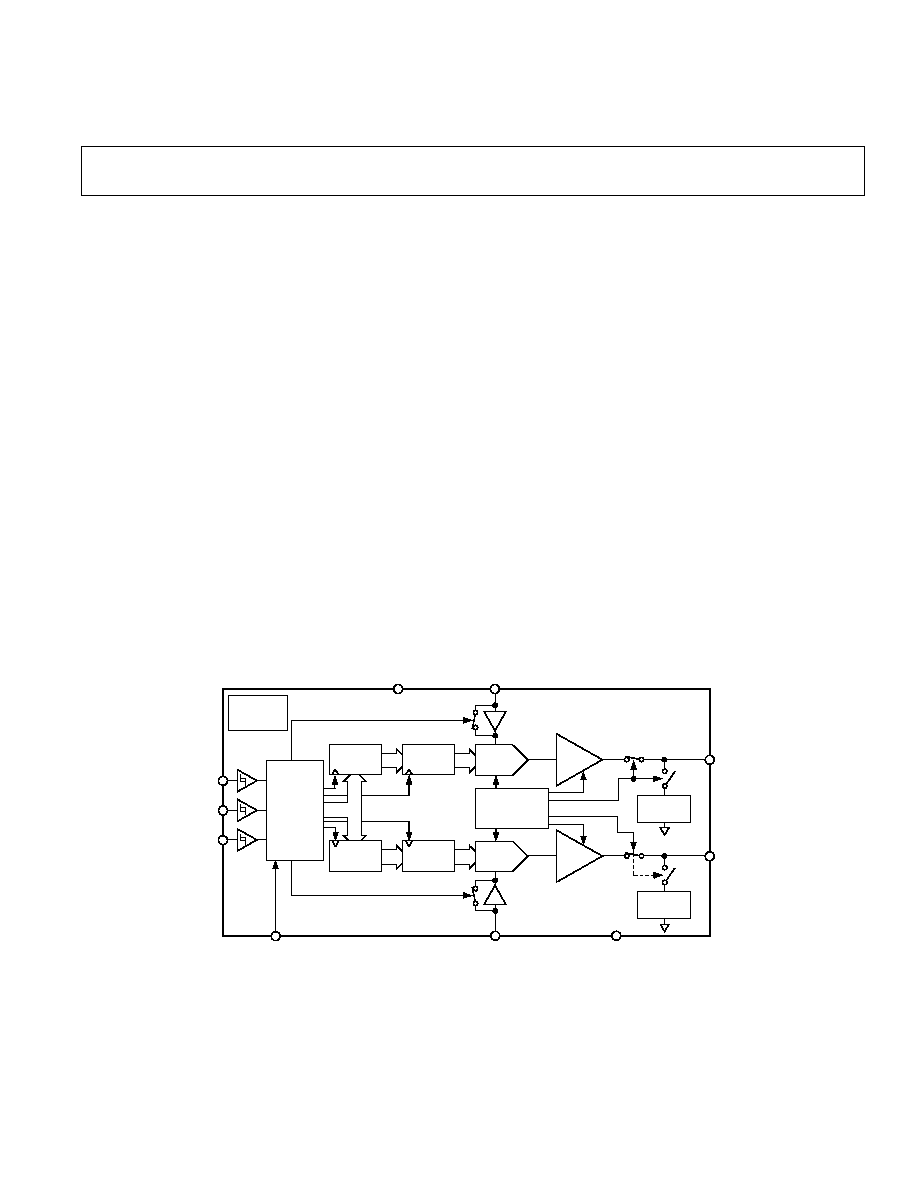
FUNCTIONAL BLOCK DIAGRAM
BUFFER
RESISTOR
NETWORK
POWER-DOWN
LOGIC
RESISTOR
NETWORK
BUFFER
STRING
DAC
STRING
DAC
AD5302/AD5312/AD5322
V
OUT
A
V
OUT
B
V
DD
V
REF
A
V
REF
B
INPUT
REGISTER
INPUT
REGISTER
DAC
REGISTER
DAC
REGISTER
INTERFACE
LOGIC
SYNC
SCLK
DIN
LDAC
GND
POWER-ON
RESET
FEATURES
AD5302: Two 8-Bit Buffered DACs in One Package
AD5312: Two 10-Bit Buffered DACs in One Package
AD5322: Two 12-Bit Buffered DACs in One Package
10-Lead SOIC Package
Micropower Operation: 300 A @ 5 V (Including
Reference Current)
Power-Down to 200 nA @ 5 V, 50 nA @ 3 V
+2.5 V to +5.5 V Power Supply
Double-Buffered Input Logic
Guaranteed Monotonic By Design Over All Codes
Buffered/Unbuffered Reference Input Options
0V
REF
Output Voltage
Power-On-Reset to Zero Volts
Simultaneous Update of DAC Outputs via
LDAC
Low Power Serial Interface with Schmitt-Triggered
Inputs
On-Chip Rail-to-Rail Output Buffer Amplifiers
APPLICATIONS
Portable Battery-Powered Instruments
Digital Gain and Offset Adjustment
Programmable Voltage and Current Sources
Programmable Attenuators
GENERAL DESCRIPTION
The AD5302/AD5312/AD5322 are dual 8-, 10- and 12-bit buff-
ered voltage output DACs in a 10-lead
µ
SOIC package that
operate from a single +2.5 V to +5.5 V supply consuming
230
µ
A at 3 V. Their on-chip output amplifiers allow the outputs
to swing rail-to-rail with a slew rate of 0.7 V/
µ
s. The AD5302/
AD5312/AD5322 utilize a versatile 3-wire serial interface which
operates at clock rates up to 30 MHz and is compatible with
standard SPITM, QSPITM, MICROWIRETM and DSP interface
standards.
The references for the two DACs are derived from two reference
pins (one per DAC). The reference inputs may be configured as
buffered or unbuffered inputs. The outputs of both DACs may
be updated simultaneously using the asynchronous
LDAC in-
put. The parts incorporate a power-on-reset circuit that ensures
that the DAC outputs power-up to 0 V and remain there until a
valid write takes place to the device. The parts contain a power-
down feature that reduces the current consumption of the
devices to 200 nA at 5 V (50 nA at 3 V) and provides software-
selectable output loads while in power-down mode.
The low power consumption of these parts in normal operation
make them ideally suited to portable battery operated equip-
ment. The power consumption is 1.5 mW at 5 V, 0.7 mW at
3 V, reducing to 1
µ
W in power-down mode.
*Patent Pending; protected by U.S. Patent No. 5684481.
SPI and QSPI are trademarks of Motorola, Inc.
MICROWIRE is a trademark of National Semiconductor Corporation.

REV. 0
2
AD5302/AD5312/AD5322SPECIFICATIONS
(V
DD
= +2.5 V to +5.5 V; V
REF
= +2 V; R
L
= 2 k
to GND; C
L
= 200 pF to GND; all specifications T
MIN
to T
MAX
unless otherwise noted.)
B Version
2
Parameter
1
Min
Typ
Max
Units
Conditions/Comments
DC PERFORMANCE
3, 4
AD5302
Resolution
8
Bits
Relative Accuracy
±
0.15
±
1
LSB
Differential Nonlinearity
±
0.02
±
0.25
LSB
Guaranteed Monotonic by Design Over All Codes
AD5312
Resolution
10
Bits
Relative Accuracy
±
0.5
±
3
LSB
Differential Nonlinearity
±
0.05
±
0.5
LSB
Guaranteed Monotonic by Design Over All Codes
AD5322
Resolution
12
Bits
Relative Accuracy
±
2
±
12
LSB
Differential Nonlinearity
±
0.2
±
1
LSB
Guaranteed Monotonic by Design Over All Codes
Offset Error
±
0.4
±
3
% of FSR
See Figures 2 and 3
Gain Error
±
0.15
±
1
% of FSR
See Figures 2 and 3
Lower Deadband
10
60
mV
See Figures 2 and 3
Offset Error Drift
5
12
ppm of FSR/
°
C
Gain Error Drift
5
5
ppm of FSR/
°
C
Power Supply Rejection Ratio
5
60
dB
V
DD
=
±
10%
DC Crosstalk
5
30
µ
V
DAC REFERENCE INPUTS
5
V
REF
Input Range
1
V
DD
V
Buffered Reference Mode
0
V
DD
V
Unbuffered Reference Mode
V
REF
Input Impedance
>10
M
Buffered Reference Mode
180
k
Unbuffered Reference Mode, Input Impedance = R
DAC
Reference Feedthrough
90
dB
Frequency = 10 kHz
Channel-to-Channel Isolation
80
dB
Frequency = 10 kHz
OUTPUT CHARACTERISTICS
5
Minimum Output Voltage
6
0.001
V min
This is a measure of the minimum and maximum
Maximum Output Voltage
6
V
DD
0.001
V max
drive capability of the output amplifier.
DC Output Impedance
0.5
Short Circuit Current
50
mA
V
DD
= +5 V
20
mA
V
DD
= +3 V
Power-Up Time
2.5
µ
s
Coming Out of Power-Down Mode. V
DD
= +5 V
5
µ
s
Coming Out of Power-Down Mode. V
DD
= +3 V
LOGIC INPUTS
5
Input Current
±
1
µ
A
V
IL
, Input Low Voltage
0.8
V
V
DD
= +5 V
±
10%
0.6
V
V
DD
= +3 V
±
10%
0.5
V
V
DD
= +2.5 V
V
IH
, Input High Voltage
2.4
V
V
DD
= +5 V
±
10%
2.1
V
V
DD
= +3 V
±
10%
2.0
V
V
DD
= +2.5 V
Pin Capacitance
2
3.5
pF
POWER REQUIREMENTS
V
DD
2.5
5.5
V
I
DD
Specification Is Valid for All DAC Codes
I
DD
(Normal Mode)
Both DACs Active and Excluding Load Currents
V
DD
= +4.5 V to +5.5 V
300
450
µ
A
Both DACs in Unbuffered Mode. V
IH
= V
DD
and
V
DD
= +2.5 V to +3.6 V
230
350
µ
A
V
IL
= GND. In Buffered Mode, extra current is
typically x
µ
A per DAC where x = 5
µ
A + V
REF
/R
DAC
.
I
DD
(Full Power-Down)
V
DD
= +4.5 V to +5.5 V
0.2
1
µ
A
V
DD
= +2.5 V to +3.6 V
0.05
1
µ
A
NOTES
1
See Terminology.
2
Temperature range: B Version: 40
°
C to +105
°
C.
3
DC specifications tested with the outputs unloaded.
4
Linearity is tested using a reduced code range: AD5302 (Code 8 to 248); AD5312 (Code 28 to 995); AD5322 (Code 115 to 3981).
5
Guaranteed by design and characterization, not production tested.
6
In order for the amplifier output to reach its minimum voltage, Offset Error must be negative. In order for the amplifier output to reach its maximum voltage,
V
REF
= V
DD
and "Offset plus Gain" Error must be positive.
Specifications subject to change without notice.
REV. 0
3
AD5302/AD5312/AD5322
AC CHARACTERISTICS
1
(V
DD
= +2.5 V to +5.5 V; R
L
= 2 k
to GND; C
L
= 200 pF to GND; all specifications T
MIN
to T
MAX
unless
otherwise noted.)
B Version
3
Parameter
2
Min
Typ
Max
Units
Conditions/Comments
Output Voltage Settling Time
V
REF
= V
DD
= +5 V
AD5302
6
8
µ
s
1/4 Scale to 3/4 Scale Change (40 Hex to C0 Hex)
AD5312
7
9
µ
s
1/4 Scale to 3/4 Scale Change (100 Hex to 300 Hex)
AD5322
8
10
µ
s
1/4 Scale to 3/4 Scale Change (400 Hex to C00 Hex)
Slew Rate
0.7
V/
µ
s
Major-Code Transition Glitch Energy
12
nV-s
1 LSB Change Around Major Carry (011 . . . 11 to 100 . . . 00)
Digital Feedthrough
0.10
nV-s
Analog Crosstalk
0.01
nV-s
DAC-to-DAC Crosstalk
0.01
nV-s
Multiplying Bandwidth
200
kHz
V
REF
= 2 V
±
0.1 V p-p. Unbuffered Mode
Total Harmonic Distortion
70
dB
V
REF
= 2.5 V
±
0.1 V p-p. Frequency = 10 kHz
NOTES
1
Guaranteed by design and characterization, not production tested.
2
See Terminology.
3
Temperature range: B Version: 40
°
C to +105
°
C.
Specifications subject to change without notice.
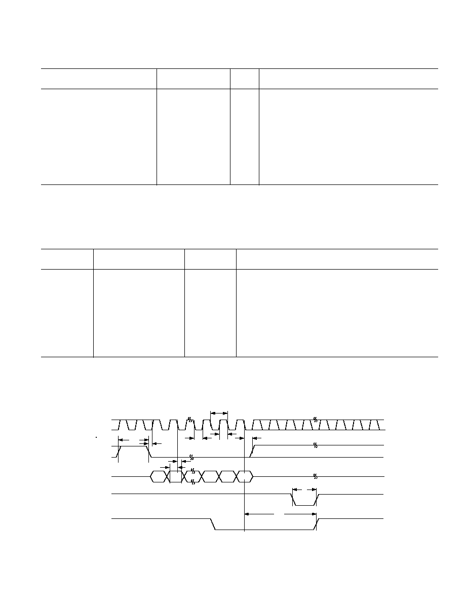
TIMING CHARACTERISTICS
1, 2, 3
Limit at T
MIN
, T
MAX
Parameter
(B Version)
Units
Conditions/Comments
t
1
33
ns min
SCLK Cycle Time
t
2
13
ns min
SCLK High Time
t
3
13
ns min
SCLK Low Time
t
4
0
ns min
SYNC to SCLK Active Edge Setup Time
t
5
5
ns min
Data Setup Time
t
6
4.5
ns min
Data Hold Time
t
7
0
ns min
SCLK Falling Edge to
SYNC Rising Edge
t
8
100
ns min
Minimum
SYNC High Time
t
9
20
ns min
LDAC Pulsewidth
t
10
20
ns min
SCLK Falling Edge to
LDAC Rising Edge
NOTES
1
Guaranteed by design and characterization, not production tested.
2
All input signals are specified with tr = tf = 5 ns (10% to 90% of V
DD
) and timed from a voltage level of (V
IL
+ V
IH
)/2.
3
See Figure 1.
Specifications subject to change without notice.
(V
DD
= +2.5 V to +5.5 V; all specifications T
MIN
to T
MAX
unless otherwise noted)
SCLK
SYNC
DIN*
t
2
t
3
t
5
t
6
t
7
t
4
DB15
t
1
DB0
t
9
t
10
LDAC
LDAC
*SEE PAGE 11 FOR DESCRIPTION OF INPUT REGISTER
t
8
Figure 1. Serial Interface Timing Diagram
REV. 0
AD5302/AD5312/AD5322
4
CAUTION
ESD (electrostatic discharge) sensitive device. Electrostatic charges as high as 4000 V readily
accumulate on the human body and test equipment and can discharge without detection.
Although the AD5302/AD5312/AD5322 features proprietary ESD protection circuitry, perma-
nent damage may occur on devices subjected to high energy electrostatic discharges. Therefore,
proper ESD precautions are recommended to avoid performance degradation or loss of functionality.
WARNING!
ESD SENSITIVE DEVICE
ABSOLUTE MAXIMUM RATINGS
1, 2
(T
A
= +25
°
C unless otherwise noted)
V
DD
to GND . . . . . . . . . . . . . . . . . . . . . . . . . . . 0.3 V to +7 V
Digital Input Voltage to GND . . . . . . . . . 0.3 V to V
DD
+ 0.3 V
Reference Input Voltage to GND . . . . . 0.3 V to V
DD
+ 0.3 V
V
OUT
A, V
OUT
B
to GND . . . . . . . . . . . . . 0.3 V to V
DD
+ 0.3 V
Operating Temperature Range
Industrial (B Version) . . . . . . . . . . . . . . . . 40
°
C to +105
°
C
Storage Temperature Range . . . . . . . . . . . . . 65
°
C to +150
°
C
Junction Temperature (T
J
Max) . . . . . . . . . . . . . . . . . . +150
°
C
10-Lead
µ
SOIC Package
Power Dissipation . . . . . . . . . . . . . . . . . . . (T
J
MaxT
A
)/
JA
JA
Thermal Impedance . . . . . . . . . . . . . . . . . . . . . 206
°
C/W
JC
Thermal Impedance . . . . . . . . . . . . . . . . . . . . . . 44
°
C/W
Lead Temperature, Soldering
Vapor Phase (60 sec) . . . . . . . . . . . . . . . . . . . . . . . +215
°
C
Infrared (15 sec) . . . . . . . . . . . . . . . . . . . . . . . . . . . +220
°
C
NOTES
1
Stresses above those listed under Absolute Maximum Ratings may cause perma-
nent damage to the device. This is a stress rating only; functional operation of the
device at these or any other conditions above those listed in the operational sections
of this specification is not implied. Exposure to absolute maximum rating condi-
tions for extended periods may affect device reliability.
2
Transient currents of up to 100 mA will not cause SCR latch-up.
ORDERING GUIDE
Temperature
Package
Package
Branding
Model
Range
Description
Option
Information
AD5302BRM
40
°
C to +105
°
C
µ
SOIC
RM-10
D5B
AD5312BRM
40
°
C to +105
°
C
µ
SOIC
RM-10
D6B
AD5322BRM
40
°
C to +105
°
C
µ
SOIC
RM-10
D7B
PIN CONFIGURATION
TOP VIEW
(Not to Scale)
10
9
8
7
6
1
2
3
4
5
LDAC
V
DD
V
REF
B
V
REF
A
V
OUT
A
GND
DIN
SCLK
SYNC
V
OUT
B
AD5302/
AD5312/
AD5322

REV. 0
AD5302/AD5312/AD5322
5
PIN FUNCTION DESCRIPTIONS
Pin No.
Mnemonic
Function
1
LDAC
Active low control input that transfers the contents of the input registers to their respective DAC regis-
ters. Pulsing this pin low allows either or both DAC registers to be updated if the input registers have new
data. This allows simultaneous update of both DAC outputs
2
V
DD
Power Supply Input. These parts can be operated from +2.5 V to +5.5 V and the supply should be de-
coupled to GND.
3
V
REF
B
Reference Input Pin for DAC B. This is the reference for DAC B. It may be configured as a buffered or
an unbuffered input, depending on the BUF bit in the control word of DAC B. It has an input range
from 0 V to V
DD
in unbuffered mode and from 1 V to V
DD
in buffered mode.
4
V
REF
A
Reference Input Pin for DAC A. This is the reference for DAC A. It may be configured as a buffered or
an unbuffered input depending on the BUF bit in the control word of DAC A. It has an input range from
0 V to V
DD
in unbuffered mode and from 1 V to V
DD
in buffered mode.
5
V
OUT
A
Buffered Analog Output Voltage from DAC A. The output amplifier has rail-to-rail operation.
6
V
OUT
B
Buffered Analog Output Voltage from DAC B. The output amplifier has rail-to-rail operation.
7
SYNC
Active Low Control Input. This is the frame synchronization signal for the input data. When
SYNC goes
low, it powers on the SCLK and DIN buffers and enables the input shift register. Data is transferred in
on the falling edges of the following 16 clocks. If
SYNC is taken high before the 16th falling edge, the
rising edge of
SYNC acts as an interrupt and the write sequence is ignored by the device.
8
SCLK
Serial Clock Input. Data is clocked into the input shift register on the falling edge of the serial clock in-
put. Data can be transferred at rates up to 30 MHz. The SCLK input buffer is powered down after each
write cycle.
9
DIN
Serial Data Input. This device has a 16-bit input shift register. Data is clocked into the register on the
falling edge of the serial clock input. The DIN input buffer is powered down after each write cycle.
10
GND
Ground reference point for all circuitry on the part.
TERMINOLOGY
RELATIVE ACCURACY
For the DAC, relative accuracy or Integral Nonlinearity (INL)
is a measure of the maximum deviation, in LSBs, from a straight
line passing through the actual endpoints of the DAC transfer
function. A typical INL vs. code plot can be seen in Figure 4.
DIFFERENTIAL NONLINEARITY
Differential Nonlinearity (DNL) is the difference between the
measured change and the ideal 1 LSB change between any two
adjacent codes. A specified differential nonlinearity of
±
1 LSB
maximum ensures monotonicity. This DAC is guaranteed
monotonic by design. A typical DNL vs. code plot can be seen
in Figure 7.
OFFSET ERROR
This is a measure of the offset error of the DAC and the output
amplifier. It is expressed as a percentage of the full-scale range.
GAIN ERROR
This is a measure of the span error of the DAC. It is the devia-
tion in slope of the actual DAC transfer characteristic from the
ideal expressed as a percentage of the full-scale range.
OFFSET ERROR DRIFT
This is a measure of the change in offset error with changes in
temperature. It is expressed in (ppm of full-scale range)/
°
C.
GAIN ERROR DRIFT
This is a measure of the change in gain error with changes in tem-
perature. It is expressed in (ppm of full-scale range)/
°
C.
MAJOR-CODE TRANSITION GLITCH ENERGY
Major-code transition glitch energy is the energy of the impulse
injected into the analog output when the code in the DAC regis-
ter changes state. It is normally specified as the area of the glitch
in nV-secs and is measured when the digital code is changed by
1 LSB at the major carry transition (011 . . . 11 to 100 . . . 00 or
100 . . . 00 to 011 . . . 11).
DIGITAL FEEDTHROUGH
Digital feedthrough is a measure of the impulse injected into the
analog output of the DAC from the digital input pins of the
device, but is measured when the DAC is not being written to
(
SYNC held high). It is specified in nV-secs and is measured
with a full-scale change on the digital input pins, i.e., from all 0s
to all 1s and vice versa.
ANALOG CROSSTALK
This is the glitch impulse transferred to the output of one DAC
due to a change in the output of the other DAC. It is measured
by loading one of the input registers with a full-scale code change
(all 0s to all 1s and vice versa) while keeping
LDAC high. Then
pulse
LDAC low and monitor the output of the DAC whose
digital code was not changed. The area of the glitch is expressed
in nV-secs.