/home/web/doc/html/ad/164222
AD532
Internally Trimmed
Integrated Circuit Multiplier
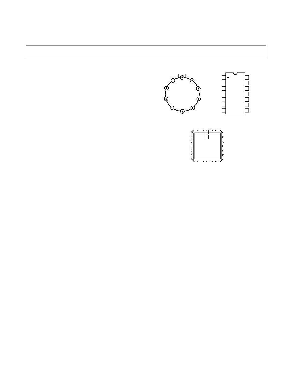
PIN CONFIGURATIONS
TOP VIEW
(Not to Scale)
14
13
12
11
10
9
8
1
2
3
4
5
6
7
NC = NO CONNECT
Z
+V
S
AD532
OUT
Y
1
V
S
Y
2
NC
V
OS
NC
GND
NC
X
2
X
1
NC
TOP VIEW
(Not to Scale)
20 19
1
2
3
18
14
15
16
17
4
5
6
7
8
9
10 11 12
13
NC = NO CONNECT
V
S
Y
2
OUT
NC
AD532
NC
NC
NC
V
OS
NC
NC
NC
GND
Z
X
1
NC
NC
+V
S
NC
Y
1
X
2
Y
1
Y
2
V
OS
GND
X
2
X
1
V
S
OUT
Z
+V
S
TOP VIEW
(Not to Scale)
AD532
FEATURES
Pretrimmed to 1.0% (AD532K)
No External Components Required
Guaranteed 1.0% max 4-Quadrant Error (AD532K)
Diff Inputs for (X
1
X
2
) (Y
1
Y
2
)/10 V Transfer Function
Monolithic Construction, Low Cost
APPLICATIONS
Multiplication, Division, Squaring, Square Rooting
Algebraic Computation
Power Measurements
Instrumentation Applications
Available in Chip Form
PRODUCT DESCRIPTION
The AD532 is the first pretrimmed single chip monolithic multi-
plier/divider. It guarantees a maximum multiplying error of
± 1.0% and a ± 10 V output voltage without the need for any
external trimming resistors or output op amp. Because the
AD532 is internally trimmed, its simplicity of use provides design
engineers with an attractive alternative to modular multipliers,
and its monolithic construction provides significant advantages
in size, reliability and economy. Further, the AD532 can be used
as a direct replacement for other IC multipliers that require
external trim networks.
FLEXIBILITY OF OPERATION
The AD532 multiplies in four quadrants with a transfer func-
tion of (X
1
X
2
)(Y
1
Y
2
)/10 V, divides in two quadrants with
a 10 V Z/(X
1
X
2
) transfer function, and square roots in one
quadrant with a transfer function of
± 10 V Z. In addition to
these basic functions, the differential X and Y inputs provide
significant operating flexibility both for algebraic computation and
transducer instrumentation applications. Transfer functions,
such as XY/10 V, (X
2
Y
2
)/10 V,
±X
2
/10 V, and 10 V Z/(X
1
X
2
),
are easily attained and are extremely useful in many modulation
and function generation applications, as well as in trigonometric
calculations for airborne navigation and guidance applications,
where the monolithic construction and small size of the AD532
offer considerable system advantages. In addition, the high
CMRR (75 dB) of the differential inputs makes the AD532
especially well qualified for instrumentation applications, as it
can provide an output signal that is the product of two transducer-
generated input signals.
GUARANTEED PERFORMANCE OVER TEMPERATURE
The AD532J and AD532K are specified for maximum multiplying
errors of
± 2% and ± 1% of full scale, respectively at 25°C, and
are rated for operation from 0
°C to 70°C. The AD532S has a
maximum multiplying error of
±1% of full scale at 25°C; it is
also 100% tested to guarantee a maximum error of
± 4% at the
extended operating temperature limits of 55
°C and +125°C. All
devices are available in either the hermetically-sealed TO-100
metal can, TO-116 ceramic DIP or LCC packages. J, K, and
S grade chips are also available.
ADVANTAGES OF ON-THE-CHIP TRIMMING OF THE
MONOLITHIC AD532
1. True ratiometric trim for improved power supply rejection.
2. Reduced power requirements since no networks across sup-
plies are required.
3. More reliable since standard monolithic assembly techniques
can be used rather than more complex hybrid approaches.
4. High impedance X and Y inputs with negligible circuit loading.
5. Differential X and Y inputs for noise rejection and additional
computational flexibility.
REV. C
One Technology Way, P.O. Box 9106, Norwood, MA 02062-9106, U.S.A.
Tel: 781/329-4700
World Wide Web Site: http://www.analog.com
Fax: 781/326-8703
© Analog Devices, Inc., 2001
a
Information furnished by Analog Devices is believed to be accurate and
reliable. However, no responsibility is assumed by Analog Devices for its
use, nor for any infringements of patents or other rights of third parties
which may result from its use. No license is granted by implication or
otherwise under any patent or patent rights of Analog Devices.

2
REV. C
AD532SPECIFICATIONS
(@ 25 C, V
S
= 15 V, R
2 k V
OS
grounded, unless otherwise noted.)
AD532J
AD532K
AD532S
Model
Min
Typ
Max
Min
Typ
Max
Min
Typ
Max
Unit
MULTIPLIER PERFORMANCE
Transfer Function
(X
1
X
2
)(Y
1
Y
2
)
10 V
(X
1
X
2
)(Y
1
Y
2
)
10 V
(X
1
X
2
)(Y
1
Y
2
)
10 V
Total Error (10 V
X, Y +10 V)
±1.5
2.0
±0.7
1.0
±0.5
1.0
%
T
A
= Min to Max
±2.5
±1.5
4.0
%
Total Error vs. Temperature
±0.04
±0.03
±0.01
0.04
%/
°C
Supply Rejection (
±15 V ± 10%)
±0.05
±0.05
±0.05
%/%
Nonlinearity, X (X = 20 V p-p, Y = 10 V)
±0.8
±0.5
±0.5
%
Nonlinearity, Y (Y = 20 V p-p, X = 10 V)
±0.3
±0.2
±0.2
%
Feedthrough, X (Y Nulled,
X = 20 V p-p 50 Hz)
50
200
30
100
30
100
mV
Feedthrough, Y (X Nulled,
Y = 20 V p-p 50 Hz)
30
150
25
80
25
80
mV
Feedthrough vs. Temperature
2.0
1.0
1.0
mV p-p/
°C
Feedthrough vs. Power Supply
±0.25
±0.25
±0.25
mV/%
DYNAMICS
Small Signal BW (V
OUT
= 0.1 rms)
1
1
1
MHz
1% Amplitude Error
75
75
75
kHz
Slew Rate (V
OUT
20 p-p)
45
45
45
V/
µs
Settling Time (to 2%,
V
OUT
= 20 V)
1
1
1
µs
NOISE
Wideband Noise f = 5 Hz to 10 kHz
0.6
0.6
0.6
mV (rms)
Wideband Noise
f = 5 Hz to 5 MHz
3.0
3.0
3.0
mV (rms)
OUTPUT
Output Voltage Swing
±10
±13
±10
±13
±10
±13
V
Output Impedance (f
1 kHz)
1
1
1
Output Offset Voltage
±40
30
30
mV
Output Offset Voltage vs. Temperature
0.7
0.7
2.0
mV/
°C
Output Offset Voltage vs. Supply
±2.5
±2.5
±2.5
mV/%
INPUT AMPLIFIERS (X, Y, and Z)
Signal Voltage Range (Diff. or CM
Operating Diff)
±10
±10
±10
V
CMRR
40
50
50
dB
Input Bias Current
X, Y Inputs
3
1.5
4
1.5
4
µA
X, Y Inputs T
MIN
to T
MAX
10
8
8
µA
Z Input
±10
±5
15
±5
15
µA
Z Input T
MIN
to T
MAX
±30
±25
±25
µA
Offset Current
±0.3
±0.1
±0.1
µA
Differential Resistance
10
10
10
M
DIVIDER PERFORMANCE
Transfer Function (X
l
> X
2
)
10 V Z/(X
1
X
2
)
10 V Z/(X
1
X
2
)
10 V Z/(X
1
X
2
)
Total Error
(V
X
= 10 V, 10 V
V
Z
+10 V)
±2
±1
±1
%
(V
X
= 1 V, 10 V
V
Z
+10 V)
±4
±3
±3
%
SQUARE PERFORMANCE
Transfer Function
(X
1
X
2
)
10 V
2
(X
1
X
2
)
10 V
2
(X
1
X
2
)
10 V
2
Total Error
±0.8
±0.4
±0.4
%
SQUARE ROOTER PERFORMANCE
Transfer Function
10 V Z
10 V Z
10 V Z
Total Error (0 V
V
Z
10 V)
±1.5
±1.0
±1.0
%
POWER SUPPLY SPECIFICATIONS
Supply Voltage
Rated Performance
±15
±15
±15
V
Operating
±10
18
±10
18
±10
±22
V
Supply Current
Quiescent
4
6
4
6
4
6
mA
PACKAGE OPTIONS
TO-116 (D-14)
AD532JD
AD532KD
AD532SD
TO-100 (H-10A)
AD532JH
AD532KH
AD532SH
LCC (E-20A)
AD532SE/883B
Specifications subject to change without notice.
Specifications shown in boldface are tested on all production units at final
electrical test. Results from those tests are used to calculate outgoing quality
levels. All min and max specifications are guaranteed, although only those shown
in boldface are tested on all production units.
THERMAL CHARACTERISTICS
H-10A:
JC
= 25
°C/W;
JA
= 150
°C/W
E-20A:
JC
= 22
°C/W;
JA
= 85
°C/W
D-14:
JC
= 22
°C/W;
JA
= 85
°C/W
3
REV. C
AD532
ORDERING GUIDE
Temperature
Package
Package
Model
Ranges
Descriptions
Options
AD532JD
0
°C to 70°C
Side Brazed DIP
D-14
AD532JD/+
0
°C to 70°C
Side Brazed DIP
D-14
AD532KD
0
°C to 70°C
Side Brazed DIP
D-14
AD532KD/+
0
°C to 70°C
Side Brazed DIP
D-14
AD532JH
0
°C to 70°C
Header
H-10A
AD532KH
0
°C to 70°C
Header
H-10A
AD532JCHIPS
0
°C to 70°C
Chip
AD532SD
55
°C to +125°C
Side Brazed DIP
D-14
AD532SD/883B
55
°C to +125°C
Side Brazed DIP
D-14
JM38510/13903BCA 55
°C to +125°C
Side Brazed DIP
D-14
AD532SE/883B
55
°C to +125°C
LCC
E-20A
AD532SH
55
°C to +125°C
Header
H-10A
AD532SH/883B
55
°C to +125°C
Header
H-10A
JM38510/13903BIA
55
°C to +125°C
Header
H-10A
AD532SCHIPS
55
°C to +125°C
Chip
CHIP DIMENSIONS AND BONDING DIAGRAM
Contact factory for latest dimensions.
Dimensions shown in inches and (mm).
0.062
(1.575)
X
1
X
2
GND
V
OS
Y
2
Y
1
V
S
Z
0.107
(2.718)
V
S
OUTPUT
X
X
1
X
2
Y
1
Y
2
V
X
V
Y
R
R
Z
OUTPUT
V
OS
R
10R
V
OUT
=
(X
1
X
2
) (Y
1
Y
2
)
10V
(WITH Z TIED TO OUTPUT)
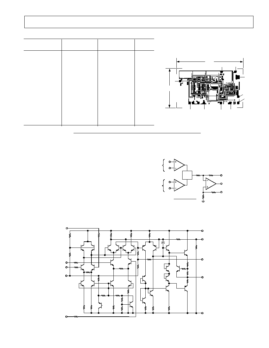
Figure 1. Functional Block Diagram
FUNCTIONAL DESCRIPTION
The functional block diagram for the AD532 is shown in Figure
1, and the complete schematic in Figure 2. In the multiplying
and squaring modes, Z is connected to the output to close the
feedback around the output op amp. (In the divide mode, it is
used as an input terminal.)
The X and Y inputs are fed to high impedance differential
amplifiers featuring low distortion and good common-mode
rejection. The amplifier voltage offsets are actively laser trimmed
to zero during production. The product of the two inputs is
resolved in the multiplier cell using Gilbert's linearized trans-
conductance technique. The cell is laser trimmed to obtain
V
OUT
= (X
1
X
2
)(Y
1
Y
2
)/10 volts. The built-in op amp is used
to obtain low output impedance and make possible self-contained
operation. The residual output voltage offset can be zeroed at
V
OS
in critical applications . . . otherwise the V
OS
pin should
be grounded.
X
2
X
1
Y
1
COM
R2
R34
R9
R1
Q1
Q2
Q3
Q4
Q5
Q6
R3
R6
R8
R16
Q7 Q8
Q14 Q15
Q9
Q10
R13
Y
2
R18
R4
R5
R10
R32
Q28
Q11
Q12
R11
R19
R14
R12
R15
Q13
Q16 Q17
R23
R20
R22
R21
C1
Q21
R27
Q25
V
S
Z
R33
V
OS
OUTPUT
R30
R28
R29
R31
Q26
Q27
Q22
Q23
Q24
R26
R25
R24
Q20
Q19
Q18
V
S
CAN
Figure 2. Schematic Diagram
AD532
4
REV. C
AD532 PERFORMANCE CHARACTERISTICS
Multiplication accuracy is defined in terms of total error at
25
°C with the rated power supply. The value specified is in
percent of full scale and includes X
IN
and Y
IN
nonlinearities,
feedback and scale factor error. To this must be added such
application-dependent error terms as power supply rejection,
common-mode rejection and temperature coefficients (although
worst case error over temperature is specified for the AD532S).
Total expected error is the rms sum of the individual compo-
nents since they are uncorrelated.
Accuracy in the divide mode is only a little more complex. To
achieve division, the multiplier cell must be connected in the
feedback of the output op amp as shown in Figure 13. In this
configuration, the multiplier cell varies the closed loop gain of the
op amp in an inverse relationship to the denominator voltage.
Thus, as the denominator is reduced, output offset, bandwidth
and other multiplier cell errors are adversely affected. The divide
error and drift are then
m
× 10 V/X
1
X
2
) where
m
represents
multiplier full-scale error and drift, and (X
1
X
2
) is the absolute
value of the denominator.
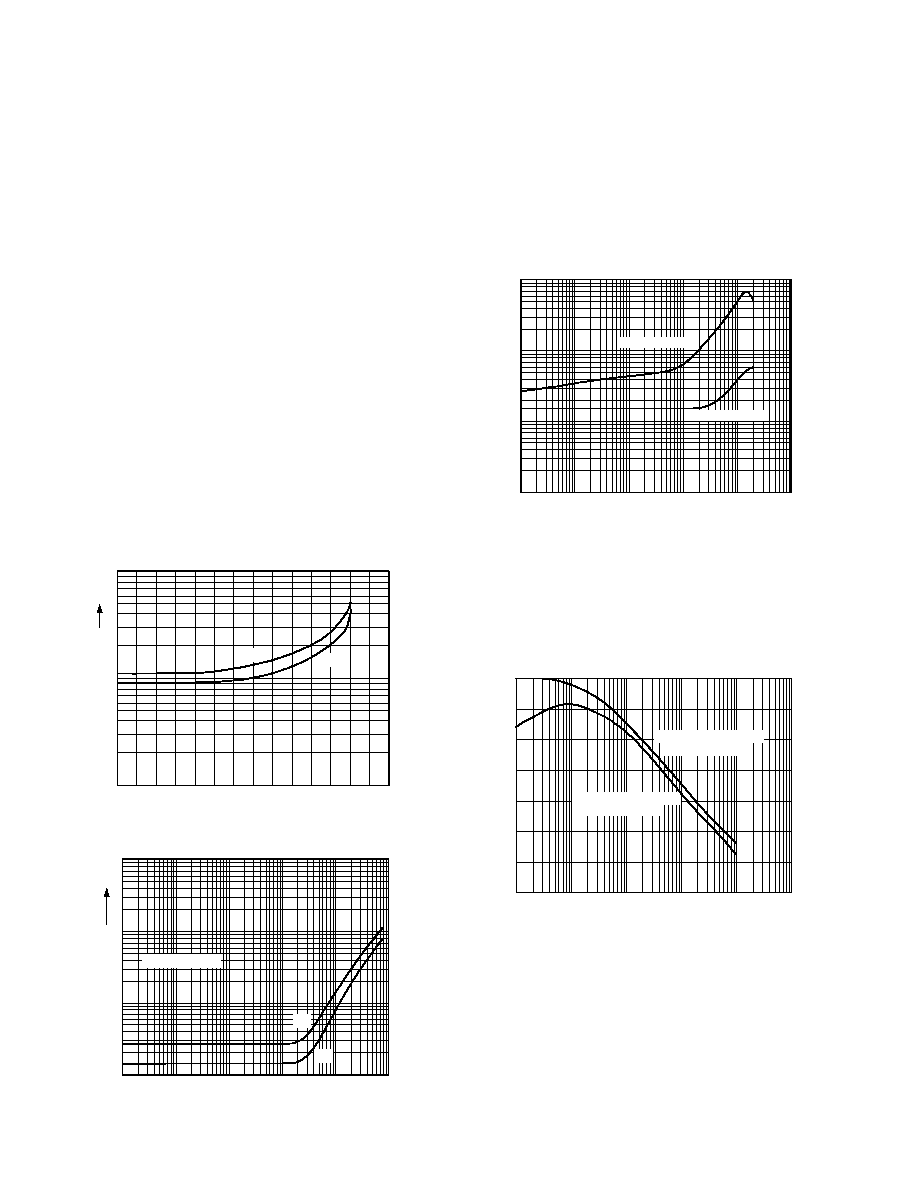
NONLINEARITY
Nonlinearity is easily measured in percent harmonic distortion.
The curves of Figures 3 and 4 characterize output distortion as
a function of input signal level and frequency respectively, with
one input held at plus or minus 10 V dc. In Figure 4 the sine
wave amplitude is 20 V (p-p).
PEAK SIGNAL AMPLITUDE Volts
PERCENT DISTORTION
1.0
1
2
10
X
IN
Y
IN
4
5
8
0.1
0.01
3
6
7
9
11
12
13
14
Figure 3. Percent Distortion vs. Input Signal
X
IN
Y
IN
20V p-p SIGNAL
FREQUENCY Hz
100
10
0.1
10
1M
100
PERCENT DISTORTION
1.0
1k
10k
100k
Figure 4. Percent Distortion vs. Frequency
AC FEEDTHROUGH
AC feedthrough is a measure of the multiplier's zero suppression.
With one input at zero, the multiplier output should be zero
regardless of the signal applied to the other input. Feedthrough
as a function of frequency for the AD532 is shown in Figure 5. It
is measured for the condition V
X
= 0, V
Y
= 20 V (p-p) and V
Y
= 0,
V
X
= 20 V (p-p) over the given frequency range. It consists
primarily of the second harmonic and is measured in millivolts
peak-to-peak.
FEEDTHROUGH
mV
FREQUENCY Hz
1000
100
1
100
10M
1k
10
10k
100k
1M
Y FEEDTHROUGH
X FEEDTHROUGH
Figure 5. Feedthrough vs. Frequency
COMMON-MODE REJECTION
The AD532 features differential X and Y inputs to enhance its
flexibility as a computational multiplier/divider. Common-mode
rejection for both inputs as a function of frequency is shown in
Figure 6. It is measured with X
1
= X
2
= 20 V (p-p), (Y
1
Y
2
) =
10 V dc and Y
1
= Y
2
= 20 V (p-p), (X
1
X
2
) = 10 V dc.
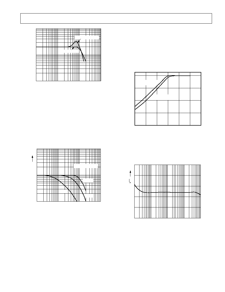
FREQUENCY Hz
0
10M
1M
100
1k
10k
100k
CMRR
dB
20
10
30
40
50
60
70
X COMMON-MODE REJ
(Y
1
Y
2
) 10V
Y COMMON-MODE REJ
(X
1
X
2
) 10V
Figure 6. CMRR vs. Frequency
5
REV. C
AD532
FREQUENCY Hz
1M
10k
100k
10M
AMPLITUDE
Volts
0.01
0.1
1.0
R
L
2k C
L
0pF
R
L
2k C
L
1000pF
Figure 7. Frequency Response, Multiplying
DYNAMIC CHARACTERISTICS
The closed loop frequency response of the AD532 in the multi-
plier mode typically exhibits a 3 dB bandwidth of 1 MHz and
rolls off at 6 dB/octave thereafter. Response through all inputs is
essentially the same as shown in Figure 7. In the divide mode,
the closed loop frequency response is a function of the absolute
value of the denominator voltage as shown in Figure 8.
Stable operation is maintained with capacitive loads to 1000 pF
in all modes, except the square root for which 50 pF is a safe
upper limit. Higher capacitive loads can be driven if a 100
resistor is connected in series with the output for isolation.
FREQUENCY Hz
1M
10k
100k
10M
AMPLITUDE
Volts
0.1
1.0
10
V
Z
0.1 V
X
SIN T
V
X
10V
V
X
5V
V
X
1V
Figure 8. Frequency Response, Dividing
POWER SUPPLY CONSIDERATIONS
Although the AD532 is tested and specified with
± 15 V dc
supplies, it may be operated at any supply voltage from
±10 V
to
±18 V for the J and K versions, and ±10 V to ±22 V for the
S version. The input and output signals must be reduced pro-
portionately to prevent saturation; however, with supply voltages
below
±15 V, as shown in Figure 9. Since power supply sensitiv-
ity is not dependent on external null networks as in other
conventionally nulled multipliers, the power supply rejection
ratios are improved from 3 to 40 times in the AD532.
POWER SUPPLY VOLTAGE Volts
10
PEAK SIGNAL VOLTAGE
Volts
12
10
8
6
4
12
14
16
18
20
22
SATURATED OUTPUT
SWING
MAX X OR Y INPUT
FOR 1% LINEARITY
Figure 9. Signal Swing vs. Supply
NOISE CHARACTERISTICS
All AD532s are screened on a sampling basis to assure that
output noise will have no appreciable effect on accuracy. Typi-
cal spot noise vs. frequency is shown in Figure 10.
SPOT NOISE
V/ Hz
1
2
3
4
5
FREQUENCY Hz
0
10
100
1k
10k
100k
Figure 10. Spot Noise vs. Frequency