Document Outline
- FEATURES
- APPLICATIONS
- FUNCTIONAL BLOCK DIAGRAM
- GENERAL DESCRIPTION
- ˛ˇ
- ˛ˇ
- ˛ˇ
- ˛ˇ
- ˛ˇ
- ˛ˇ
- ˛ˇ
- ˛ˇ
2.5 V to 5.5 V, 250 µA, 2-Wire Interface
Dual-Voltage Output, 8-/10-/12-Bit DACs
AD5337/AD5338/AD5339
Rev. A
Information furnished by Analog Devices is believed to be accurate and reliable.
However, no responsibility is assumed by Analog Devices for its use, nor for any
infringements of patents or other rights of third parties that may result from its use.
Specifications subject to change without notice. No license is granted by implication
or otherwise under any patent or patent rights of Analog Devices. Trademarks and
registered trademarks are the property of their respective owners.
One Technology Way, P.O. Box 9106, Norwood, MA 02062-9106, U.S.A.
Tel: 781.329.4700
www.analog.com
Fax: 781.326.8703
© 2004 Analog Devices, Inc. All rights reserved.
FEATURES
AD5337
2 buffered 8-bit DACs in 8-lead MSOP
AD5338, AD5338-1
2 buffered 10-bit DACs in 8-lead MSOP
AD5339
2 buffered 12-bit DACs in 8-lead MSOP
Low power operation: 250 mA @ 3 V, 300 mA @ 5 V
2-wire (I
2
CÆcompatible) serial interface
2.5 V to 5.5 V power supply
Guaranteed monotonic by design over all codes
Power-down to 80 nA @ 3 V, 200 nA @ 5 V
3 power-down modes
Double-buffered input logic
Output range: 0 V to V
REF
Power-on reset to 0 V
Simultaneous update of outputs (LDAC function)
Software clear facility
Data readback facility
On-chip rail-to-rail output buffer amplifiers
Temperature range -40∞C to +105∞C
APPLICATIONS
Portable battery-powered instruments
Digital gain and offset adjustment
Programmable voltage and current sources
Programmable attenuators
Industrial process control
GENERAL DESCRIPTION
AD5337/AD5338/AD5339 are dual 8-, 10-, and 12-bit buffered
voltage output DACs in an 8-lead MSOP package, which
operate from a single 2.5 V to 5.5 V supply, consuming 250 µA
at 3 V. On-chip output amplifiers allow rail-to-rail output swing
with a slew rate of 0.7 V/µs. A 2-wire serial interface operates at
clock rates up to 400 kHz. This interface is SMBus-compatible
at V
DD
< 3.6 V. Multiple devices can be placed on the same bus.
The references for the two DACs are derived from one reference
pin. The outputs of all DACs may be updated simultaneously
using the software LDAC function. The parts incorporate a
power-on reset circuit that ensures that the DAC outputs power
up to 0 V and remain there until a valid write to the device
takes place. A software clear function resets all input and DAC
registers to 0 V. A power-down feature reduces the current
consumption of the devices to 200 nA @ 5 V (80 nA @ 3 V).
The low power consumption of these parts in normal operation
makes them ideally suited to portable battery-operated
equipment. The power consumption is typically 1.5 mW at 5 V
and 0.75 mW at 3 V, reducing to 1 µW in power-down mode.
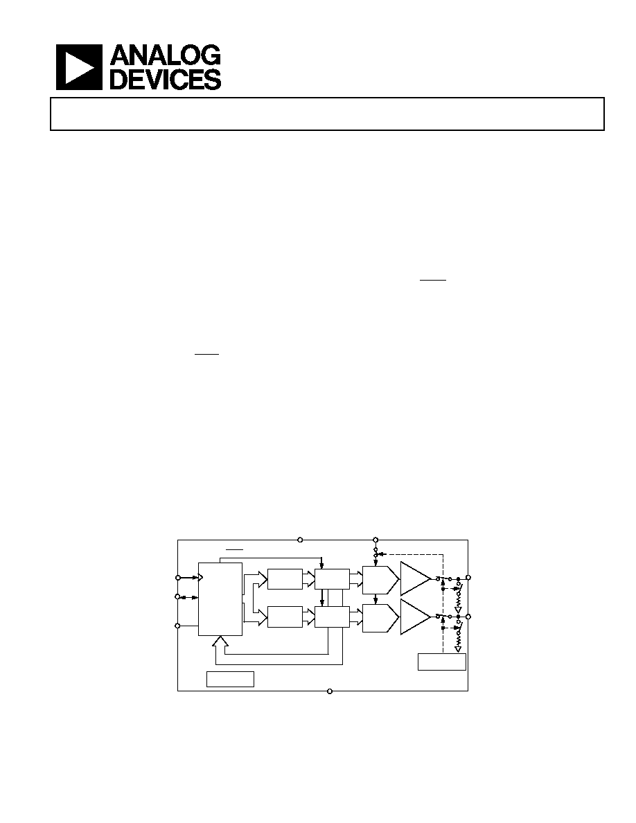
FUNCTIONAL BLOCK DIAGRAM
SCL
INTERFACE
LOGIC
INPUT
REGISTER
V
OUT
A
BUFFER
DAC
REGISTER
STRING
DAC A
V
DD
REFIN
INPUT
REGISTER
V
OUT
B
BUFFER
DAC
REGISTER
POWER-ON
RESET
POWER-DOWN
LOGIC
LDAC
STRING
DAC B
A0
SDA
GND
AD5337/AD5338/AD5339
03756-A
-
001
Figure 1.

AD5337/AD5338/AD5339
Rev. A | Page 2 of 24
TABLE OF CONTENTS
Specifications..................................................................................... 3
AC Characteristics........................................................................ 5
Timing Characteristics ................................................................ 6
Absolute Maximum Ratings............................................................ 7
ESD Caution.................................................................................. 7
Pin Configuration and Function Descriptions............................. 8
Terminology ...................................................................................... 9
Typical Performance Characteristics ........................................... 11
Functional Description .................................................................. 15
Digital-to-Analog Converter Section ...................................... 15
Resistor String ............................................................................. 15
DAC Reference Inputs ............................................................... 15
Output Amplifier........................................................................ 15
Power-on Reset ........................................................................... 15
Serial Interface ............................................................................ 15
Write Operation.......................................................................... 17
Read Operation........................................................................... 18
Double-Buffered Interface ........................................................ 19
Power-Down Modes .................................................................. 19
Applications..................................................................................... 20
Typical Application Circuit....................................................... 20
Bipolar Operation....................................................................... 20
Multiple Devices on One Bus ................................................... 20
Product as a Digitally Programmable Window Detector ..... 21
Coarse and Fine Adjustment Capabilities............................... 21
Power Supply Decoupling ......................................................... 21
Outline Dimensions ....................................................................... 24
Ordering Guide .......................................................................... 24
REVISION HISTORY
10/04--Changed Data Sheet from Rev. 0 to Rev. A
Updated Format..................................................................Universal
Added AD5338-1................................................................Universal
Changes to Specifications ................................................................ 4
Updated Outline Dimensions ....................................................... 24
Changes to Ordering Guide .......................................................... 24
11/03--Rev. 0: Initial Version

AD5337/AD5338/AD5339
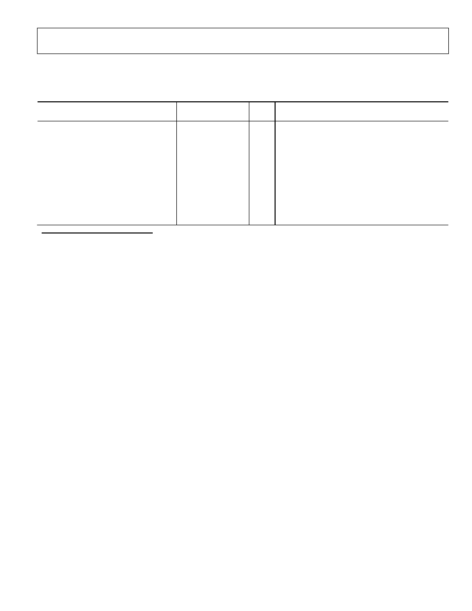
Rev. A | Page 3 of 24
SPECIFICATIONS
V
DD
= 2.5 V to 5.5 V; V
REF
= 2 V; R
L
= 2 k to GND; C
L
= 200 pF to GND; all specifications T
MIN
to T
MAX
, unless otherwise noted.
Table 1.
Grade A
Grade B
Parameter
1
Min
Typ Max
Min
Typ Max
Unit B
Version
2
Conditions/Comments
DC PERFORMANCE
3, 4
AD5337
Resolution
8
8
Bits
Relative
Accuracy
±0.15 ±1
±0.15 ±0.5 LSB
Differential
Nonlinearity
±0.02 ±0.25
±0.02 ±0.25
LSB
Guaranteed monotonic by design over
all codes
AD5338
Resolution
10 10 Bits
Relative
Accuracy ±0.5 ±4 ±0.5 ±2 LSB
Differential
Nonlinearity
±0.05 ±0.5
±0.05 ±0.50
LSB
Guaranteed monotonic by design over
all codes
AD5339
Resolution
12 12 Bits
Relative
Accuracy ±2 ±16
±2 ±8
LSB
Differential
Nonlinearity
±0.2 ±1 ±0.2 ±1 LSB
Guaranteed monotonic by design over
all codes
Offset Error
±0.4
±3
±0.4
±3
% of FSR
Gain Error
±0.15
±1
±0.15
±1
% of FSR
Lower
Deadband
20 60
20 60
mV
Lower deadband exists only if offset error
is negative
Offset Error Drift
5
-12
-12
ppm of
FSR/∞C
Gain Error Drift
5
-5 -5
ppm of
FSR/∞C
Power Supply Rejection
Ratio
5
-60
-60
dB
V
DD
= ±10%
DC Crosstalk
5
200 200 µV
R
L
= 2 k to GND or V
DD
DAC REFERENCE INPUTS
5
V
REF
Input Range
0.25
V
DD
0.25
V
DD
V
V
REF
Input Impedance
37
45
37
45
k
Normal operation
>10
>10
M
Power-down
mode
Reference
Feedthrough
-90
-90
dB
Frequency
=
10
kHz
OUTPUT CHARACTERISTICS
5
Minimum Output Voltage
6
0.001
0.001
V
This is a measure of the minimum and
maximum drive capabilities of the output
amplifier.
Maximum Output
Voltage
6
V
DD
-
0.001
V
DD
-
0.001
V
DC Output Impedance
0.5
0.5
Short Circuit Current
25
25
mA
V
DD
= 5 V
16 16 mA V
DD
= 3 V
Power-Up
Time
2.5 2.5 µs
Coming out of power-down mode.
V
DD
= 5 V
5
5 µs
Coming out of power-down mode.
V
DD
= 3 V

AD5337/AD5338/AD5339
Rev. A | Page 4 of 24
Grade A
Grade B
Parameter
1
Min
Typ Max
Min
Typ Max
Unit B
Version
2
Conditions/Comments
LOGIC INPUTS (A0)
5
Input
Current
±1
±1
µA
V
IL
, Input Low Voltage
0.8
0.8
V
V
DD
= 5 V ±10%
0.6
0.6
V V
DD
= 3 V ±10%
0.5
0.5
V V
DD
= 2.5 V
V
IH
, Input High Voltage
2.4
2.4
V
V
DD
= 5 V ±10%
2.1
2.1
V V
DD
= 3 V ±10%
2.0
2.0
V V
DD
= 2.5 V
Pin
Capacitance
3
3 pF
LOGIC INPUTS (SCL, SDA)
5
V
IH
, Input High Voltage
0.7
V
DD
V
DD
+
0.3
0.7
V
DD
V
DD
+
0.3
V
SMBus-compatible at V
DD
< 3.6 V
V
IL
, Input Low Voltage
-0.3
+0.3
V
DD
≠0.3
+0.3
V
DD
V
SMBus-compatible at V
DD
< 3.6 V
I
IN
, Input Leakage Current
±1
±1
µA
V
HYST
, Input Hysteresis
0.05
V
DD
0.05
V
DD
V
C
IN
, Input Capacitance
8
8
pF
Glitch
Rejection
50
50
ns Input
filtering suppresses noise spikes of
less than 50 ns
LOGIC OUTPUT (SDA)
5
V
OL,
Output Low Voltage
0.4
0.4
V
I
SINK
= 3 mA
0.6
0.6
V I
SINK
= 6 mA
Three-State Leakage
Current
±1
±1
µA
Three-State Output
Capacitance
8
8 pF
POWER
REQUIREMENTS
V
DD
2.5
5.5
2.5
5.5
V
I
DD
(Normal Mode)
7
V
IH
= V
DD
and V
IL
= GND
V
DD
= 4.5 V to 5.5 V
300
375
300
375
µA
V
DD
= 2.5 V to 3.6 V
250
350
250
350
µA
I
DD
(Power-Down
Mode)
V
IH
= V
DD
and V
IL
= GND
V
DD
= 4.5 V to 5.5 V
0.2
1.0
0.2
1.0
µA
I
DD
= 4 µA (max) during 0 readback
on SDA
V
DD
= 2.5 V to 3.6 V
0.08
1.00
0.08
1.00
µA
I
DD
= 1.5 µA (max) during 0 readback
on SDA
1
For explanations of the specific parameters, see the Termin
section.
ology
2
Temperature range: (A and B versions): -40∞C to +105∞C; typical at 25∞C.
3
DC specifications tested with the outputs unloaded.
4
Linearity is tested using a reduced code range: AD5337 (Codes 8 to 248); AD5338, AD5338-1 (Codes 28 to 995); AD5339 (Codes 115 to 3981).
5
Guaranteed by design and characterization; not production tested.
6
For the amplifier output to reach its minimum voltage, offset error must be negative; to reach its maximum voltage, V
REF
= V
DD
and offset plus gain error must be
positive.
7
I
DD
specification is valid for all DAC codes. Interface inactive. All DACs active and excluding load currents.
AD5337/AD5338/AD5339
Rev. A | Page 5 of 24
AC CHARACTERISTICS
1
V
DD
= 2.5 V to 5.5 V; R
L
= 2 k to GND; C
L
= 200 pF to GND; all specifications T
MIN
to T
MAX
, unless otherwise noted.
Table 2.
A and B Versions
2
Parameter
3
Min Typ Max Unit Conditions/Comments
Output Voltage Settling Time
V
REF
= V
DD
= 5 V
AD5337
6
8
µs
1/4 scale to 3/4 scale change (0x40 to 0xC0)
AD5338
7
9
µs
1/4 scale to 3/4 scale change (0x100 to 0x300)
AD5339
8
10
µs
1/4 scale to 3/4 scale change (0x400 to 0xC00)
Slew Rate
0.7
V/µs
Major-Code Transition Glitch Energy
12
nV-s
1 LSB change around major carry
Digital Feedthrough
1
nV-s
Digital Crosstalk
1
nV-s
DAC-to-DAC Crosstalk
3
nV-s
Multiplying Bandwidth
200
kHz
V
REF
= 2 V ± 0.1 V p-p
Total Harmonic Distortion
-70
dB
V
REF
= 2.5 V ± 0.1 V p-p. Frequency = 10 kHz
1
Guaranteed by design and characterization; not production tested.
2
Temperature range: A and B versions: -40∞C to +105∞C; typical at 25∞C.
3
For explanations of the specific parameters, see the Termin
section.
ology