 | ÐлекÑÑоннÑй компоненÑ: AD5380 | СкаÑаÑÑ:  PDF PDF  ZIP ZIP |
Äîêóìåíòàöèÿ è îïèñàíèÿ www.docs.chipfind.ru
Preliminary Technical Data
PRELIMINARY TECHNICAL DATA
REV. PrF 09/2003
Information furnished by Analog Devices is believed to be accurate and
reliable. However, no responsibility is assumed by Analog Devices for its
use, nor for any infringements of patents or other rights of third parties
which may result from its use. No license is granted by implication or
otherwise under any patent or patent rights of Analog Devices.
a
AD5380
One Technology Way, P.O. Box 9106, Norwood, MA 02062-9106, U.S.A.
Tel: 781/329-4700
World Wide Web Site: http://www.analog.com
Fax: 781/326-8703
© Analog Devices, Inc., 2003
14
DAC
REG
0
VOUT 0
LDAC
CLR
WR/(DCEN/AD1)
FIFO EN
BUSY
INTERFACE
CONTROL
LOGIC
AVDD (X5)
DVDD (X3)
DGND (X3)
+
14
INPUT
REG
0
14
m REG0
c REG0
14
14
14
AGND (X5)
+
INPUT
REG
6
14
m REG6
14
14
14
X
+
-
c REG6
14
14
DAC 6
DAC
REG
6
VOUT 5
+
INPUT
REG
7
14
m REG7
c REG7
14
VOUT 1
VOUT 4
14
DAC
REG
7
14
VOUT 7
VOUT 8
VOUT 38
VOUT 2
VOUT 3
AD5380
X5
X
X
VOUT 6
14
14
DAC 0
DAC 7
+
INPUT
REG
1
14
m REG1
14
14
14
X
c REG1
14
14
DAC 1
DAC
REG
1
.
.
.
.
.
.
.
.
.
.
.
.
.
.
.
.
.
.
+
-
+
-
+
-
.
.
.
POWER-ON
RESET
FIFO
+
STATE
MACHINE
+
CONTROL
LOGIC
RESET
DB10
DB0
.
DB13 /(DIN/SDA)
A0
A5
CS/(SYNC/AD0)
REG0
REG1
SER/PAR
2.5V
Reference
REFOUT/ REFIN
DB12 /(SCLK/SCL)
PD
R
R
R
R
R
R
R
R
SIGNAL GND (X5)
REFGND
DAC GND (X5)
SDO(A/B)
DB11 /(SPI/I2C)
39 -TO-1
MUX
VOUT 0 .......... VOUT 38
VOUT 39 / MON_OUT
40-Channel, 3V/5V Single Supply,
14-Bit, Voltage-Output DAC
F E A T U R E S
G u a r a n t e e d M o n o t o n i c
INL Error: ±4LSB max
On-Chip 1.25/2.5V, 10ppm/°C Reference
Temperature Range: -40°C to +85°C
Rail to Rail Output Amplifier
Package Type: 100-lead LQFP (14mm x 14mm)
User Interfaces:
Parallel,
Serial (SPI, QSPI, Microwire and DSP compatible
featuring Data Readback)
I2C Compatible Interface
INTEGRATED FUNCTIONS
Channel Monitor
Simultaneous Output Update via
LDAC
LDAC
LDAC
LDAC
LDAC
Clear Function to User Programmable Code
Amplifier Boost Mode to Optimize Slew Rate
User Programmable Offset and Gain Adjust
Toggle Mode: Enables Squarewave Generation
A P P L I C A T I O N S
Variable Optical Attenuators (VOA)
Level Setting
Optical Microelectromechanical Systems (MEMs)
Control Systems
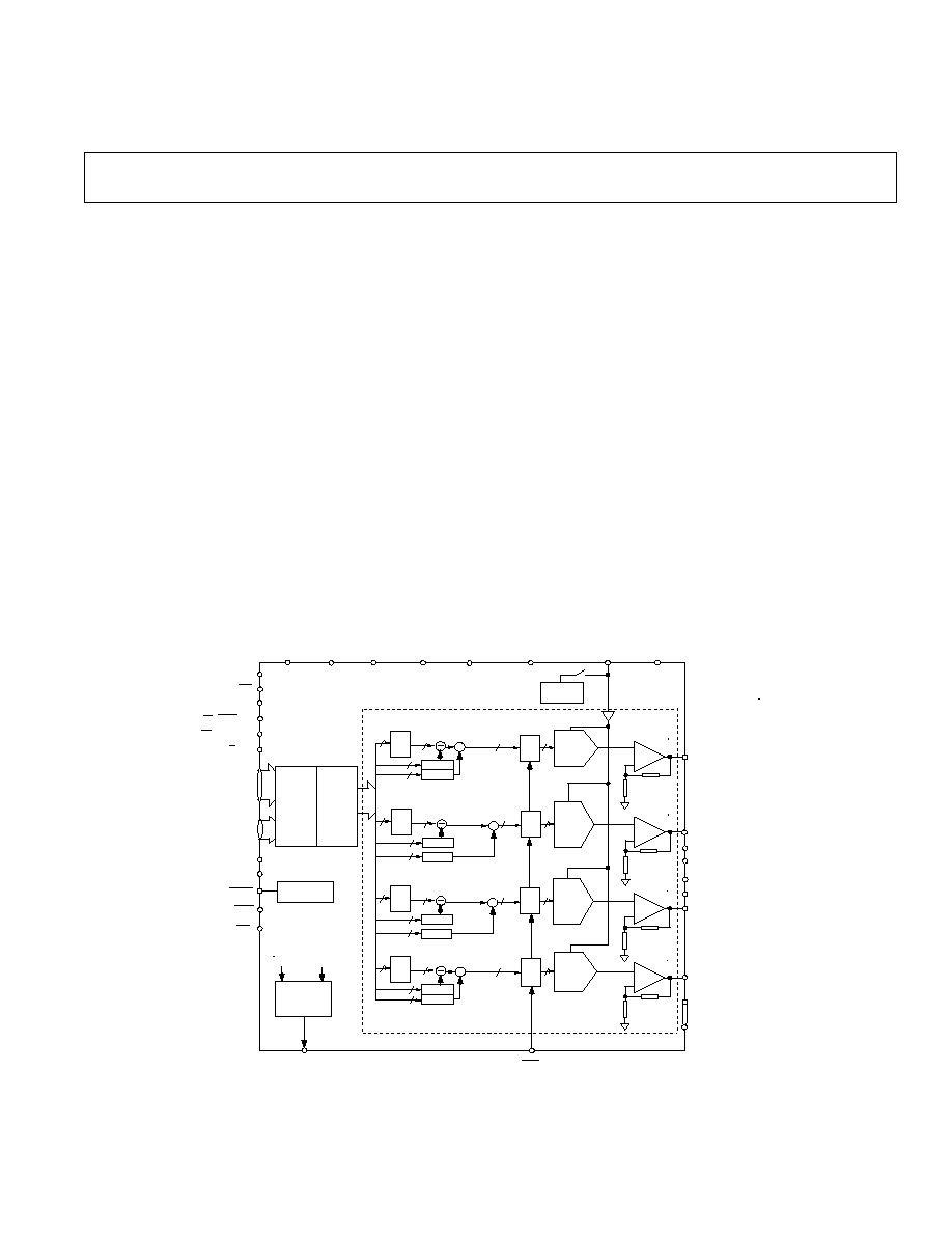
GENERAL DESCRIPTION
The AD5380 is a complete single supply, 40-channel, 14-
bit DAC available in 100-lead LQFP package. All
40-channels have an on-chip output amplifier with rail-to-
rail operation. The AD5380 includes an internal 1.25/
2.5V, 10ppm/°C reference, an on-chip channel monitor
function that multiplexes the analog outputs to a common
MON_OUT pin for external monitoring and an output
amplifier boost mode that allows the amplifier settling
time to be optimized. The AD5380 contains a double
buffered parallel interface featuring a
WR pulse width of
20ns, a serial interface compatible with SPI
TM
, QSPI
TM
,
MICROWIRE
TM
and DSP interface standards with
interface speeds in excess of 30MHz and an I2C
compatible interface supporting 400kHz data transfer rate.
An input register followed by a DAC register provides
double buffering allowing the DAC outputs to be updated
independantly or simultaneously using the
LDAC input.
Each channel has a programmable gain and offset adjust
register allowing the user to fully calibrate any DAC Channel.
Power consumption is typically 0.3mA/channel.
*Protected by U.S. Patent Nos. 5,969,657; other patents pending.
SPI and QSPI are Trademarks of Motorola, Inc.
MICROWIRE is a Trademark of National Semiconductor Corporation.
FUNCTIONAL BLOCK DIAGRAM

PRELIMINARY TECHNICAL DATA
REV. PrF 09/2003
2
Parameter
AD5380-5
1
Units
Test Conditions/Comments
A C C U R A C Y
Resolution
1 4
Bits
Relative Accuracy
3
± 4
LSB max
Differential Nonlinearity
- 1 / + 2
LSB max
Guaranteed Monotonic Over Temp
Zero-Scale Error
± 1 0
mV max
Offset Error
± 1 0
mV max
Measured at code 32 in the linear region
Offset Error TC
± 5
uV/°C typ
Gain Error
± 0 . 0 2
% FSR max
Gain Temperature Coefficient
2
2 0
ppm FSR/°C typ
DC Crosstalk
2
0 . 5
L S B m a x
R E F E R E N C E I N P U T / O U T P U T
REFERENCE INPUT
2
Reference Input Voltage
2 . 5
V
±1% for Specified Performance
DC Input Impedance
1
M
min
Typically 100 M
Input Current
± 1 0
µA max
Typically ±30 nA
Reference Range
1/V
DD
/2
V min/max
REFERENCE OUTPUT
4
Output Voltage
2.495/2.505
V min/max
At Ambient
1.248/1.252
V min/max
Reference TC
± 1 0
ppm/°C typ
OUTPUT CHARACTERISTICS
2
Output Voltage Range
3
0/AV
DD
V min/max
Short Circuit Current
4 0
mA max
Load Current
± 1
mA max
Capacitive Load Stability
R
L
=
2 0 0
pF max
R
L
=5k
T B D
pF max
DC Output Impedance
0 . 5
max
MONITOR PIN
Output Impedance
5 0 0
typ
Tristate Leakage Current
1 0 0
nA typ
LOGIC INPUTS (EXCEPT SDA/SCL)
2
DV
DD
= 2.7 V to 5.5 V
V
IH
, Input High Voltage
2
V min
V
IL
, Input Low Voltage
0 . 8
V max
Input Current
± 1 0
µA max
Total for All Pins. T
A
=T
MIN
to T
MAX
Pin Capacitance
1 0
pF max
LOGIC INPUTS (SCL, SDA ONLY)
V
IH
, Input High Voltage
0.7 DV
DD
V min
SMBus-Compatible at DV
DD
< 3.6 V
V
IL
, Input Low Voltage
0.3 DV
DD
V max
SMBus-Compatible at DV
DD
< 3.6 V
I
IN
, Input Leakage Current
±1
µ A
V
HYST
, Input Hysteresis
0.05 DV
DD
V
C
IN
, Input Capacitance
8
pF
Glitch Rejection
5 0
ns
Input filtering suppresses noise spikes of
less than 50 ns.
LOGIC OUTPUTS (
BUSY, SDO)
2
V
OL,
Output Low Voltage
0 . 4
V max
DV
DD
= 5V ± 10%, Sinking 200µA
V
OH,
Output High Voltage
DV
DD
-1
V min
DV
DD
= 5V ± 10%, Sourcing
2 0 0 µ A
V
OL,
Output Low Voltage
0 . 4
V max
DV
DD
= 2.7V to 3.6V, Sinking
2 0 0 µ A
V
OH,
Output High Voltage
DV
DD
-0.5
V min
DV
DD
= 2.7V to 3.6V, S o u r c i n g
2 0 0 µ A
High Impedance Leakage Current
± 1
µA max
SDO Only
High Impedance Output Capacitance
5
pF typ
SDO Only
LOGIC OUTPUT (SDA)
2
V
OL
, Output Low Voltage
0.4
V max
I
SINK
= 3 mA
0.6
V max
I
SINK
= 6 mA
Three-State Leakage Current
±1
µ A
Three-State Output Capacitance
8
pF
AD5380-5SPECIFICATIONS
(AV
DD
= 4.5V to 5.5V ; DV
DD
=2.7V to 5.5V, AGND=DGND = 0 V; C
L
= 200 pF to AGND; R
L
=
5k
; External REFIN=2.5V; All specifications T
MIN
to T
MAX
unless otherwise noted.)

PRELIMINARY TECHNICAL DATA
REV. PrF 09/2003
3
AD5380
POWER REQUIREMENTS
AV
DD
4 . 5 / 5 . 5
V min/max
DV
DD
2 . 7 / 5 . 5
V min/max
Power Supply Sensitivity
2
Mid Scale/
V
DD
- 8 5
dB typ
AI
DD
0 . 5
mA/Channelmax
Outputs Unloaded. Boost Off.
XXmA typ
AI
DD
0 . 5 7
mA/Channelmax
Outputs Unloaded. Boost On.
XXmA typ
DI
DD
5
mA max
V
IH
= DV
DD
, V
IL
= DGND.
XXmA typ
AI
DD
(Power Down)
5
uA max
DI
DD
(Power Down)
5
uA max
Power Dissipation
1 2 5
mW max
Outputs Unloaded.
N O T E S
1
AD5380-5 is calibrated using an external 2.5V reference. Temperature range for All Versions: -40°C to +85°C
2
Guaranteed by characterization. Not production tested.
3
Accuracy guaranteed from Vout = 10mV to AV
DD
-50mV
4
Default on the AD5380-5 is 2.5V.Programmable to 1.25V via CR12 in the AD5380 control register but operating the AD5380-5 with
a 1.25V reference will lead to degraded accuracy specifications.
Specifications subject to change without notice.
AD5380-5 SPECIFICATIONS
(AV
DD
= 4.5V to 5.5V ; DV
DD
=2.7V to 5.5V, AGND=DGND = 0 V;
C
L
= 200 pF to AGND; R
L
= 5k
; External REFIN=2.5V;
All specifications T
MIN
to T
MAX
unless otherwise noted.)
Parameter
All
Units
Test Conditions/Comments
DYNAMIC PERFORMANCE
Output Voltage Settling Time
2
Boost Mode Off, CR11=0
AD5380
8
µs typ
1/4 Scale to 3/4 Scale Change settling to ±1LSB.
1 0
µs max
Output Voltage Settling Time
2
Boost Mode On, CR11=1
AD5380
3
µs typ
1/4 Scale to 3/4 Scale Change settling to ±1LSB.
5
µs max
Slew Rate
2
0 . 7
V/µs typ
Boost Mode Off, CR11=0
1 . 5
V/µs typ
Boost Mode On, CR11=1
Digital-to-Analog Glitch Energy
1 2
nV-s typ
Glitch Impulse Peak Amplitude
5
mV max
Channel-to-Channel Isolation
1 0 0
dB typ
See Terminology
DAC-to-DAC Crosstalk
1 0
nV-s typ
See Terminology
Digital Crosstalk
1 0
nV-s typ
Digital Feedthrough
1
nV-s typ
Effect of Input Bus Activity on DAC Output Under Test
Output Noise 0.1 to 10Hz
8
uV p-p typ
Output Noise Spectral Density
@ 1 kHz
1 5 0
nV/(Hz)
1/2
typ
@ 10 kHz
100
nV/(Hz)
1/2
typ
1
Guaranteed by design and characterization, not production tested.
2
The Settling Time and Slew Rate can be programmed via the Current Boost Control bit (CR11 ) in the AD5380 Control Register.
Specifications subject to change without notice.
AC CHARACTERISTICS
1
(AV
DD
= 4.5V to 5.5V ; DV
DD
=2.7V to 5.5V; AGND = DGND= 0 V; C
L
= 5k
and
200 pF to AGND)

PRELIMINARY TECHNICAL DATA
REV. PrF 09/2003
4
Parameter
AD5380-3
1
Units
Test Conditions/Comments
A C C U R A C Y
Resolution
1 4
Bits
Relative Accuracy
3
± 4
LSB max
Differential Nonlinearity
- 1 / + 2
LSB max
Guaranteed Monotonic Over Temp
Zero-Scale Error
± 1 0
mV max
Offset Error
± 1 0
mV max
Measured at code 64 in the linear region
Offset Error TC
± 5
uV/°C typ
Gain Error
± 0 . 0 2
% FSR max
Gain Temperature Coefficient
2
2 0
ppm FSR/°C typ
DC Crosstalk
2
0 . 5
L S B m a x
R E F E R E N C E I N P U T / O U T P U T
REFERENCE INPUT
2
Reference Input Voltage
1 . 2 5
V
±1% for Specified Performance
DC Input Impedance
1
M
min
Typically 100 M
Input Current
± 1 0
µA max
Typically ±30 nA
Reference Range
1 to AV
DD
/2
V min/max
REFERENCE OUTPUT
4
Output Voltage
1.248/1.252
V min/max
At Ambient
2.495/2.505
V min/max
Reference TC
± 1 0
ppm/°C typ
OUTPUT CHARACTERISTICS
2
Output Voltage Range
3
0/AV
DD
V min/max
Short Circuit Current
4 0
mA max
Load Current
± 1
mA max
Capacitive Load Stability
R
L
=
2 0 0
pF max
R
L
=5k
T B D
pF max
DC Output Impedance
0 . 5
max
MONITOR PIN
Output Impedance
5 0 0
typ
Tristate Leakage Current
1 0 0
nA typ
LOGIC INPUTS (EXCEPT SDA/SCL)
2
DV
DD
= 2.7 V to 3.6V
V
IH
, Input High Voltage
2
V min
V
IL
, Input Low Voltage
0 . 8
V max
Input Current
± 1 0
µA max
Total for All Pins. T
A
=T
MIN
to T
MAX
Pin Capacitance
1 0
pF max
LOGIC INPUTS (SCL, SDA ONLY)
V
IH
, Input High Voltage
0.7 DV
DD
V min
SMBus-Compatible at DV
DD
< 3.6 V
V
IL
, Input Low Voltage
0.3 DV
DD
V max
SMBus-Compatible at DV
DD
< 3.6 V
I
IN
, Input Leakage Current
±1
µ A
V
HYST
, Input Hysteresis
0.05 DV
DD
V
C
IN
, Input Capacitance
8
pF
Glitch Rejection
5 0
ns
Input filtering suppresses noise spikes of
less than 50 ns.
LOGIC OUTPUTS (
BUSY, SDO)
2
V
OL,
Output Low Voltage
0 . 4
V max
Sinking 200µA
V
OH,
Output High Voltage
DV
DD
-0.5
V min
Sourcing 200µA
High Impedance Leakage Current
± 1
µA max
SDO Only
High Impedance Output Capacitance
5
pF typ
SDO Only
LOGIC OUTPUT (SDA)
2
V
OL
, Output Low Voltage
0.4
V max
I
SINK
= 3 mA
0.6
V max
I
SINK
= 6 mA
Three-State Leakage Current
±1
µ A
Three-State Output Capacitance
8
pF
AD5380-3SPECIFICATIONS
(AV
DD
= 2.7V to 3.6V ; DV
DD
=2.7V to 5.5V, AGND=DGND = 0 V; C
L
= 200 pF to AGND; R
L
=
5k
; External REFIN=1.25V; All specifications T
MIN
to T
MAX
unless otherwise noted.)

PRELIMINARY TECHNICAL DATA
REV. PrF 09/2003
5
AD5380
POWER REQUIREMENTS
AV
DD
2 . 7 / 3 . 6
V min/max
DV
DD
2 . 7 / 3 . 6
V min/max
Power Supply Sensitivity
2
Mid Scale/
V
DD
- 8 5
dB typ
AI
DD
0 . 5
mA/Channelmax
Outputs Unloaded. Boost Off.
XXmA typ
AI
DD
0 . 5 7
mA/Channelmax
Outputs Unloaded. Boost On.
XXmA typ
DI
DD
5
mA max
V
IH
= DV
DD
, V
IL
= DGND.
XXmA typ
AI
DD
(Power Down)
5
uA max
DI
DD
(Power Down)
5
uA max
Power Dissipation
1 2 5
mW max
Outputs Unloaded.
N O T E S
1
AD5380-3 is calibrated using an external 1.25V reference. Temperature range is -40°C to +85°C.
2
Guaranteed by characterization. Not production tested.
3
Accuracy guaranteed from Vout = 10mV to AV
DD
-50mV
4
Default on the AD5380-3 is 1.25V. Programmable to 2.5V via CR12 in the AD5380 control register but operating the AD5380-3 with
a 2.5V reference will lead to degraded accuracy specifications and limited input code range.
Specifications subject to change without notice.
AD5380-3SPECIFICATIONS
(AV
DD
= 2.7V to 3.6V ; DV
DD
=2.7V to 5.5V, AGND=DGND = 0 V;
C
L
= 200 pF to AGND; R
L
= 5k
; External REFIN=1.25V;
All specifications T
MIN
to T
MAX
unless otherwise noted.)
Parameter
All
Units
Test Conditions/Comments
DYNAMIC PERFORMANCE
Output Voltage Settling Time
2
Boost Mode Off, CR11=0
AD5380
8
µs typ
1/4 Scale to 3/4 Scale Change settling to ±1LSB.
1 0
µs max
Output Voltage Settling Time
2
Boost Mode On, CR11=1
AD5380
3
µs typ
1/4 Scale to 3/4 Scale Change settling to ±1LSB.
5
µs max
Slew Rate
2
0 . 7
V/µs typ
Boost Mode Off, CR11=0
1 . 5
V/µs typ
Boost Mode On, CR11=1
Digital-to-Analog Glitch Energy
1 2
nV-s typ
Glitch Impulse Peak Amplitude
5
mV max
Channel-to-Channel Isolation
1 0 0
dB typ
See Terminology
DAC-to-DAC Crosstalk
1 0
nV-s typ
See Terminology
Digital Crosstalk
1 0
nV-s typ
Digital Feedthrough
1
nV-s typ
Effect of Input Bus Activity on DAC Output Under Test
Output Noise 0.1 to 10Hz
8
uV p-p
Output Noise Spectral Density
@ 1 kHz
1 5 0
nV/(Hz)
1/2
typ
@ 10 kHz
100
nV/(Hz)
1/2
typ
1
Guaranteed by design and characterization, not production tested.
2
The Settling Time and Slew Rate can be programmed via the Current Boost Control bit (CR11 ) in the AD5380 Control Register.
Specifications subject to change without notice.
AC CHARACTERISTICS
1
(AV
DD
= 2.7V to 3.6V ; DV
DD
=2.7V to 5.5V; AGND = DGND= 0 V; C
L
= 5k
and
200 pF to AGND)
PRELIMINARY TECHNICAL DATA
REV. PrF 09/2003
6
SERIAL INTERFACE
Parameter
1,2,3
Limit at T
MIN,
T
MAX
Units
Description
t
1
33
ns min
SCLK Cycle Time
t
2
13
ns min
SCLK High Time
t
3
13
ns min
SCLK Low Time
t
4
13
ns min
SYNC Falling Edge to SCLK Falling Edge Setup
Time
t
5
4
13
ns min
24th SCLK Falling Edge to
SYNC Falling Edge
t
6
4
33
ns min
Minimum
SYNC Low Time
t
7
10
ns min
Minimum
SYNC High Time
t
7A
50
ns min
Minimum
SYNC High Time in Readback Mode
t
8
5
ns min
Data Setup Time
t
9
4.5
ns min
Data Hold Time
t
10
4,5
30
ns max
24th SCLK Falling Edge to
BUSY Falling Edge
t
11
900
ns typ
BUSY Pulse Width Low (Single Channel Update)
t
12
4
20
ns min
24th SCLK Falling Edge to
LDAC Falling Edge
t
13
20
ns min
LDAC Pulse Width Low
t
14
100
ns max
BUSY Rising Edge to DAC Output Response Time
t
15
0
ns min
BUSY Rising Edge to LDAC Falling Edge
t
16
100
ns min
LDAC
Falling Edge to
DAC Output Response Time
t
17
8
µs typ
DAC Output Settling Time, Boost Mode off.
t
18
20
ns min
CLR Pulse Width Low
t
19
12
µs max
CLR Pulse Activation Time
t
20
6,7
20
ns max
SCLK Rising Edge to SDO Valid
t
21
7
5
ns min
SCLK Falling Edge to
SYNC Rising Edge
t
22
7
8
ns min
SYNC Rising Edge to SCLK Rising Edge
t
23
7
20
ns min
SYNC Rising Edge to LDAC Falling Edge
N O T E S
1
Guaranteed by design and characterization, not production tested.
2
All input signals are specified with t
r
= t
f
= 5 ns (10% to 90% of V
CC
) and timed from a voltage level of 1.2 V.
3
See Figures 3 and 4
4
Stand-Alone Mode only.
5
This is measured with the load circuit of Figure 1a.
6
This is measured with the load circuit of Figure 1b.
7
Daisy-Chain Mode only.
Specifications subject to change without notice.
(DV
DD
= 2.7V to 5.5V ; AV
DD
=+4.5V to +5.5V or +2.7V to +3.6V; AGND= DGND = 0 V; )
All specifications T
MIN
to T
MAX
unless otherwise noted.)
TIMING CHARACTERISTICS
I
O L
200u A
I
O H
200u A
C
L
50pF
TO
O UT P UT
P IN
VOH (M IN) or
VOL (MAX)
C
L
50pF
R
L
2.2k
TO
OUTPUT
PIN
VOL
VCC
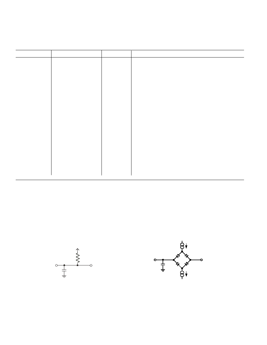
Figure 1a Load Circuit for
BUSY Timing Diagram
Figure 1b. Load Circuit for SDO Timing Diagram
(Serial Interface, Daisy-Chain mode)
PRELIMINARY TECHNICAL DATA
REV. PrF 09/2003
AD5380
7
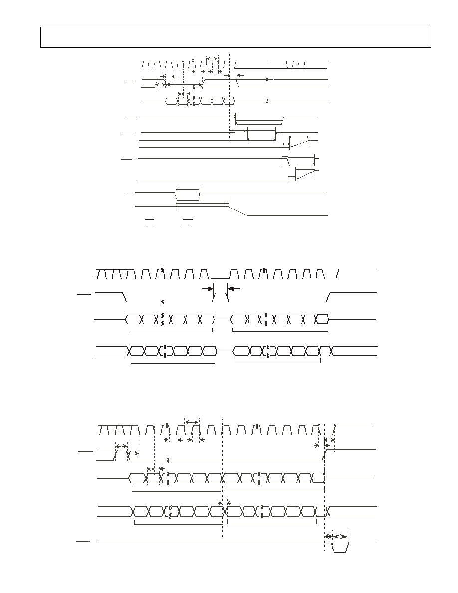
Figure 4. Serial Interface Timing Diagram (Daisy-Chain mode)
Input Word for DAC N
DB23
UNDEFINED
DB0
SDO
t20
SCLK
SYNC
DIN
DB23
t1
t4
DB23'
t21
t22
DB0'
DB0
Input Word for DAC N+1
Input Word for DAC N
24
48
t13
t3
t2
t1
t7
t8 t9
LDAC
t23
Figure 3. Serial Interface Timing Diagram (Stand-Alone mode)
SCLK
SYNC
DIN
DB23
DB0
t4
t7
t6
1
2
24
CLR
VOUT
t19
t18
24
t9
t8
t3
t2
t1
1
LDAC ACTIVE DURING BUSY
2
LDAC ACTIVE AFTER BUSY
LDAC1
t10
LDAC2
VOUT
1
t
16
VOUT
2
BUSY
t11
t12
t13
t13
t15
t14
t17
t17
t5
Selected Register Data
Clocked out.
DB23
DB0
DB23'
DB0'
48
NOP Condition
UNDEFINED
SDO
SCLK
SYNC
DIN
DB23
DB0
Input Word Specifies
Register to be Read
24
t7A
Figure 3a. Serial Interface Timing in Data Readback Mode
PRELIMINARY TECHNICAL DATA
REV. PrF 09/2003
8
AD5380
F
S C L
400
kHz max
SCL Clock Frequency
t
1
2.5
µs min
SCL Cycle Time
t
2
0.6
µs min
t
HIGH
, SCL High Time
t
3
1.3
µs min
t
LOW
, SCL Low Time
t
4
0.6
µs min
t
HD,STA
, Start/Repeated Start Condition Hold Time
t
5
100
ns min
t
SU,DAT
, Data Setup Time
t
6
3
0.9
µs max
t
HD,DAT
, Data Hold Time
0
µs min
t
HD,DAT
, Data Hold Time
t
7
0.6
µs min
t
SU,STA
, Setup Time for Repeated Start
t
8
0.6
µs min
t
SU,STO
, Stop Condition Setup Time
t
9
1.3
µs min
t
BUF
, Bus Free Time Between a STOP and a START Condition
t
10
300
ns max
t
R
, Rise Time of SCL and SDA when Receiving
0
ns min
t
R
, Rise Time of SCL and SDA when Receiving (CMOS-Com
patible)
t
11
300
ns max
t
F
, Fall Time of SDA when Transmitting
0
ns min
t
F
, Fall Time of SDA when Receiving (CMOS-Compatible)
300
ns max
t
F
, Fall Time of SCL and SDA when Receiving
20 + 0.1C
b
4
ns min
t
F
, Fall Time of SCL and SDA when Transmitting
C
B
400
pF max
Capacitive Load for Each Bus Line
TIMING CHARACTERISTICS
(DV
DD
= 2.7V to 5.5V ; AV
DD
=+4.5V to +5.5V or +2.7V to +3.6V; AGND= DGND = 0 V; )
All specifications T
MIN
to T
MAX
unless otherwise noted.)
I2C SERIAL INTERFACE
Parameter
1,2
Limit at T
MIN,
T
MAX
Units
Description
N O T E S
1
Guaranteed by design and characterization, not production tested.
2
See Figure 5
3
A master device must provide a hold time of at least 300 ns for the SDA signal (referred to the V
IH
MIN of the SCL signal) in order to bridge the
undefined region of SCL's falling edge.
4
Cb is the total capacitance of one bus line in pF. t
R
and t
F
measured between 0.3 VDD and 0.7 VDD.
SCL
SDA
START
CONDITION
t
9
t
3
t
4
t
6
t
2
t
5
t
7
t
8
t
1
t
4
t
11
t
10
REPEATED
START
CONDITION
STOP
CONDITION
Figure 5. I2C Compatible Serial Interface Timing Diagram
PRELIMINARY TECHNICAL DATA
REV. PrF 09/2003
AD5380
9
PARALLEL INTERFACE
Parameter
1,2,3
Limit at T
MIN,
T
MAX
Units
Description
t
0
4.5
ns min
REG0,REG1,Address to
WR Rising Edge Setup Time
t
1
4.5
ns min
REG0,REG1, Address to
WR Rising Edge Hold Time
t
2
20
ns min
CS Pulse Width Low
t
3
20
ns min
WR
Pulse Width Low
t
4
0
ns min
CS to WR Falling Edge Setup Time
t
5
0
ns min
WR to CS Rising Edge Hold Time
t
6
4.5
ns min
Data to
WR Rising Edge Setup Time
t
7
4.5
ns min
Data to
WR Rising Edge Hold Time
t
8
20
ns min
WR
Pulse Width High
t
9
4
430
ns min
Minimum
WR Cycle Time (Single Channel Write)
t
10
4
30
ns max
WR
Rising Edge to
BUSY Falling Edge
t
11
4,5
400
ns max
BUSY Pulse Width Low (Single Channel Update)
t
12
4
30
ns min
WR
Rising
Edge to
LDAC
Falling Edge
t
13
20
ns min
LDAC Pulse Width Low
t
14
4
100
ns max
BUSY Rising Edge
to DAC Output Response Time
t
15
20
ns min
LDAC Rising Edge
to
WR Rising Edge
t
16
0
ns min
BUSY Rising Edge to
LDAC
Falling Edge
t
17
4
100
ns min
LDAC
Falling Edge to
DAC Output Response Time
t
18
8
µs typ
DAC Output Settling Time, Boost Mode Off.
t
19
20
ns min
CLR Pulse Width Low
t
20
12
µs
max
CLR Pulse Activation Time
(DV
DD
= 2.7 V to +5.5V; AV
DD
=+4.5V to +5.5V or +2.7V to +3.6V; AGND = DGND = 0 V;
All specifications T
MIN
to T
MAX
unless otherwise noted.)
N O T E S
1
Guaranteed by design and characterization, not production tested.
2
All input signals are specified with t
r
= t
f
= 5 ns (10% to 90% of V
CC
) and timed from a voltage level of 1.2 V.
3
See Timing Diagram in Figure 6.
4
See Table XXX.
5
This is measured with the load circuit of Figure 1a.
Specifications subject to change without notice.
TIMING CHARACTERISTICS
Figure 6. Parallel Interface Timing Diagram
t4
t7
t6
DB13..DB0
t5
REG0, REG1, A5..A0
CS
LDAC1
t2
CLR
t20
t19
t3
WR
t10
LDAC2
1
LDAC ACTIVE DURING BUSY
2
LDAC ACTIVE AFTER BUSY
VOUT
1
t
17
VOUT
2
t8
BUSY
t11
t12
t13
t13
t16
t14
t18
t18
VOUT
t9
t1
t0
t15

PRELIMINARY TECHNICAL DATA
REV. PrF 09/2003
1 0
AD5380
ABSOLUTE MAXIMUM RATINGS
1,2
(T
A
= +25°C unless otherwise noted)
AV
DD
to AGND...............................................-0.3 V to +7 V
DV
DD
to DGND..............................................-0.3 V to +7 V
Digital Inputs to DGND............-0.3 V to DV
DD
+ 0.3 V
SDA/SCL to DGND..............................-0.3 V to + 7 V
Digital Outputs to DGND..........-0.3 V to DV
DD
+ 0.3 V
REFIN/REFOUT to AGND......-0.3 V to AV
DD
+ 0.3 V
AGND to DGND................................-0.3 V to +0.3 V
VOUT0-39 to AGND...............
- 0.3 V to AV
DD
+ 0.3 V
Analog Inputs to AGND............
- 0.3 V to AV
DD
+ 0.3 V
Operating Temperature Range
Commercial (B Version).......................-40°C to +85°C
Storage Temperature Range...................-65°C to +150°C
JunctionTemperature (T
J
max).............................+150°C
100-lead LQFP Package,
JA
ThermalImpedance.....................................44°C/W
Reflow Soldering
Peak Temperature......................................................230°C
NOTES:
1
Stresses above those listed under "Absolute Maximum Ratings" may cause
permanent damage to the device. This is a stress rating only, and functional
operation of the device at these or any other conditions above those listed in the
operational sections of this specification is not implied. Exposure to absolute
maximum rating conditions for extended periods may affect device reliability.
2
Transient currents of up to 100mA will not cause SCR latch-up
CAUTION
ESD (electrostatic discharge) sensitive device. Electrostatic charges as high as 4000 V readily
accumulate on the human body and test equipment and can discharge without detection.
Although the AD5380 features proprietary ESD protection circuitry, permanent damage may
occur on devices subjected to high energy electrostatic discharges. Therefore, proper ESD
precautions are recommended to avoid performance degradation or loss of functionality.
ORDERING GUIDE
Linearity
Package
Package
Model
Resolution
AV
DD
Output
Error (LSBs)
Description
Option
Range
Channels
AD5380BST-5 14-Bits
+4.5V to +5.5V
4 0
± 4
100-lead LQFP
ST-100
AD5380BST-3 14-Bits
+2.7V to +3.6V
4 0
± 4
100-lead LQFP
ST-100
Eval-AD5380EB
AD5380 Evaluation Kit
PRELIMINARY TECHNICAL DATA
REV. PrF 09/2003
AD5380
1 1
AD5380 (40-CHANNEL, 14-BIT)
PIN CONFIGURATIONS
AD5380 PIN FUNCTION DESCRIPTIONS
Mnemonic
Function
V O U T X
Buffered analog outputs for channel X. Each analog output is driven by a rail to rail output
amplifier operating at a gain of 2. Each output is capable of driving an output load of 5k to
ground. Typical output impedance is 0.5 ohms.
SIGNAL_GND(1-5)
Analog ground reference points for each group of 8 output channels. All signal_gnd pins are
tied together internally and should be connected to AGND plane as close as possible to the
AD5380.
DAC-GND (1-5)
Each group of 8 channels contains a DAC_GND pin. This is the ground reference point for
the internal 14-bit DACs.These pins shound be connected to the AGND plane.
AGND (1-5)
Analog Ground reference point. Each group of 8 channels contains an AGND pin. All
AGND pins should be connected externally to the AGND plane.
AVDD (1-5)
Analog Supply pins. Each group of 8 channels has a separate AVDD pin. These pins should
be decoupled with 0.1uF ceramic capacitors and 10uF tantalum capacitors. Operating range
for the ASD5380-5 is 4.5V to 5.5V and for the AD5380-3 is 2.7V to 3.6V
D G N D
Ground for all digital circuitry.
D V D D
Logic Power Supply; Guaranteed operating range is 2.7 V to 5.5 V. Recommended that
these pins be decoupled with 0.1uF ceramic and 10uF tantalum capacitors to DGND.
R E F - G N D
Ground Reference point for the internal reference.
R E F O U T / R E F I N
The AD5380 contains a common REFOUT/REF IN pin. When the internal reference is
selected this pin is the reference output. If the application necessitates the use of an external
reference, it can be applied to this pin and the internal reference disabled vis the control
register. The default for this pin is a reference input.
94
93
92
91
90
89
88
87
86
85
84
83
82
81
DB8
SD
OU
T(
A
/
B
)
DGND
DGND
DGND
A5
A4
A3
A2
A1
A0
DV
DD
DV
DD
DV
DD
97
96
95
C
S
/(
S
Y
N
C
/
AD
0
)
DB1
3
/
(DIN/S
DA
)
DB1
2
/
(S
CLK/S
C
L
)
DB1
1
/
(
SPI
/
I
2
C
)
DB1
0
DB9
100
99
98
5
4
3
2
7
6
9
8
1
11
10
16
15
14
13
18
17
20
19
22
21
12
24
23
25
FIFO EN
CLR
VOUT 24
VOUT 25
VOUT 26
VOUT 27
SIGNAL_GND4
DAC_GND4
AGND4
AVDD4
VOUT 28
VOUT 29
VOUT 30
VOUT 31
REF GND
REFOUT/REFIN
SIGNAL_GND1
DAC_GND1
AVDD1
VOUT 0
VOUT 1
VOUT 2
VOUT 3
VOUT 4
AGND1
26
28
27
30
29
SIGNA
L
_GND5
DA
C_
GND5
A
G
ND5
A
V
DD5
VOU
T
5
32
33
34
35
36
38
39
40
41
42
43
44
45
46
47
48
49
50
31
37
VOU
T
6
VOU
T
7
VOU
T
32
VOU
T
33
VOU
T
34
VOU
T
35
VOU
T
36
VOU
T
37
VOU
T
38
VOUT 39/M
ON_ OUT
VOU
T
8
VOU
T
9
VOU
T
10
VOU
T
11
VOU
T
12
DA
C_
GND2
SIGNA
L
_GND2
VOU
T
13
VOU
T
14
VOU
T
15
76
77
78
79
80
SER
/
P
A
R
PD
W
R
(DCE
N/A
D
1
)
L
D
A
C
B
U
S
Y
74
75
72
73
70
71
65
66
67
68
63
64
61
62
59
60
69
57
58
55
56
53
54
51
52
RESET
DB7
DB6
DB5
DB4
DB3
DB2
DB1
DB0
REG0
REG1
VOUT 23
VOUT 22
VOUT 21
VOUT 20
AVDD3
AGND3
DAC_GND3
SIGNAL_GND3
VOUT 19
VOUT 18
VOUT 17
VOUT 16
AVDD2
AGND2
PIN 1
IDENTIFIER
TOP VIEW
(Not to Scale)
AD5380

PRELIMINARY TECHNICAL DATA
REV. PrF 09/2003
1 2
AD5380
V O U T 3 9 / M O N _ O U T
This pin has a dual function, it acts a a buffered output for channel 39 in default mode but
when the monitor function is enabled this output acts as the output of a 39-to-1 channel
multiplexer which can be programmed to multiplex one of channels 0 to 38 to the
MON_OUT pin. The MON_OUT pins output impedance is typically 500 ohms and is
intended to drive a high input impedance like that exhibited by SAR ADC inputs.
S E R /
PAR.
Interface Select Input. This pin allows the user to select whether the serial or parallel
interface will be used. If it is tied high the serial interface mode is selected and pin 97 (
SPI/
I2C) is used to determine if the interface mode is SPI or I2C.
Parallel interface mode is selected when SER/
PAR is low.
CS/(SYNC/AD0)
In parallel interface mode this pin acts as Chip Select Input (level sensitive, active low).
When low the AD5380 device is selected.
Serial Interface Mode: This is the Frame Synchronisation input signal for the serial
interface. When taken low the internal counter is enabled to count the required number of
clocks before the addressed register is updated.
I2C Mode: This pin acts as a hardware address pin used in conjunction with AD1 to
determine the software address for the device on the I2C bus.
WR /(DCEN/AD1)
Multi Function pin. In parallel interface mode acts as Write enable and in serial interface
mode acts as a daisy chain enable in SPI mode and as a hardware address pin in I2C mode.
Parallel Interface Write Input (edge sensitive). The rising edge of
WR is used in conjunction
with
CS low and the address bus inputs to write to the selected device registers.
Serial Interface: Daisy-Chain Select Input (level sensitive, active high). When high this
signal is used in conjunction with SER/
PAR high to enable SPI serial interface daisy-chain
mode.
I2C Mode: This pin acts as a hardware address pin used in conjunction with AD0 to
determine the software address for this device on the I2C bus.
DB13-DB0
Parallel Data Bus. DB13 is the MSB and DB0 is the LSB of the input data word on the
AD5380
A5-A0
Parallel Address Inputs. A5 to A0 are decoded to address one of the 40 input channels on the
AD5380. Used in conjunction with the REG1 and REG0 pins to determine the destination
register for the input data.
REG1,REG0
REG1 and REG0 are used in decoding the destination registers for the input data. REG1
and REG0 are decoded to address the input data register, offset register or gain register for
the selected channel and also are used to decide the special function registers.
S D O U T / (
A/B)
Serial Data Output in serial interface mode. Tristatable CMOS output. SDO can be used
for daisy-chaining a number of devices together. Data is clocked out on SDO on the rising
edge of SCLK and is valid on the falling edge of SCLK.
When operating in parallel interface mode this pin acts as the A or B data register select
when writing data to the AD5380 data registers when toggle mode is selected (See Toggle
Mode Function). In toggle mode the LDAC is used to switch the output between the data
contained in the A and B data registers. All DAC channels contain two data registers. In
normal mode data register A is the default for data transfers.
B U S Y
Digital CMOS Output.
BUSY goes low during internal calculations of the data (x2) loaded
to the DAC data register. During this time the user can continue writing new data to further
x1, c and m registers (these are stored in a FIFO) but no further updates to the DAC
registers and DAC outputs can take place. If
LDAC is taken low while
BUSY is low this
event is stored.
BUSY also goes low during power-on-reset and when the RESET pin is
low. During this time the interface is disabled and any events on
LDAC are ignored. A
CLR operation also brings
BUSY low.
L D A C
Load DAC Logic Input (active low). If
LDAC is taken low while BUSY is inactive (high)
the contents of the input registers are transferred to the DAC registers and the DAC outputs
are updated. If
LDAC is taken low while BUSY is active and internal calculations are
taking place, the
LDAC event is stored and the DAC registers are updated when BUSY
goes inactive. However any events on
LDAC during power-on-reset or RESET are ignored.
C L R
Asynchronous Clear Input (level sensitive, active low). While
CLR is low all LDAC pulses
are ignored. When
CLR is activated all channels are updated with the data contained in the
CLR code register. BUSY is low for a duration of 12us while all channels are being
updated with the
CLR code.
R E S E T
Asynchronous Digital Reset Input (falling edge sensitive). The function of this pin is
equivalent to that of the Power-On-Reset generator. When this pin is taken low, the state-
machine initiates a reset sequence to digitally reset x1, m, c, and x2 registers to their default

PRELIMINARY TECHNICAL DATA
REV. PrF 09/2003
AD5380
1 3
power-on values. This sequence takes 300us (typ). The falling edge of
RESET initiates the
RESET process and
BUSY goes low for the duration returning high when RESET is
complete.
While BUSY is low all interfaces are disabled and all LDAC pulses are ignored.
When BUSY returns high the part resumes normal operation and the status of the RESET
pin is ignored till the next falling edge is detected.
P D
Power Down (level sensitive active high). Used to place the device in low power mode where
the device consumes less than 5uA. In power pown mode all internal analog circuitry is
placed in low power mode, the analog output will be configured as high impedance outputs
or will provide a 100k load to ground depending on how the power down mode is
configured. The serial interface remains active during power down.
F I F O _ E N
FIFO Enable (level sensitive active high). When connected to DVCC the internal FIFO is
enabled allowing the user to write to the device at full speed. FIFO is only available in
parallel interface mode. The status of the FIFO_EN pin is sampled on power-up, and also
following a CLEAR or RESET to determine if the FIFO is enabled. In either serial or I2C
interface modes the FIFO_EN pin shpould be tied low.
DB11 (SPI/
I2C)
Multi-function input pin. In parallel interface mode this pin acts as DB11 of the parallel
input data word. In serial interface mode this pin acts as serial interface mode select.
When serial interface mode is selected (SER/
PAR =1) and this input is low I2C Mode is
selected. In this mode DB12 is the serial clock (SCLK) input and DB13 is the serial data
(DIN) input.
When serial interface mode is selected (SER/
PAR =1) and this input is high SPI Mode is
selected. In this mode DB12 is the serial clock (SCL) input and DB13 is the serial data
(SDA) input.
DB12 (SCLK/SCL)
Multi-function input pin. In parallel interface mode this pin acts as DB12 of the parallel
input data word. In serial interface mode this pin acts as a serial clock input.
Serial Interface Mode: In serial interface mode data is clocked into the shift register on the
falling edge of SCLK. This operates at clock speeds up to 50 MHz.
I2C Mode: In I2C mode this pin performs the SCL function, clocking data into the device.
Data transfer rate in I2C mode is compatible with both 100kHz and 400kHz operating
modes.
DB13/(DIN/SDA)
Multi-function data input pin.
In parallel interface mode this pin acts as DB13 of the parallel input data word.
Serial Interface Mode: In serial interface mode this pin acts as the serial data input. Data
must be valid on the falling edge of SCLK.
I2C Mode: In I2C mode this pin is the serial Data pin (SDA) operating as an open drain
input/output.

PRELIMINARY TECHNICAL DATA
REV. PrF 09/2003
1 4
AD5380
TERMINOLOGY
Relative Accuracy
Relative accuracy or endpoint linearity is a measure of the
maximum deviation from a straight line passing through
the endpoints of the DAC transfer function. It is
measured after adjusting for zero-scale error and full-scale
error and is expressed in Least Significant Bits.
Differential Nonlinearity
Differential nonlinearity is the difference between the
measured change and the ideal 1 LSB change between any
two adjacent codes. A specified differential nonlinearity of
1 LSB maximum ensures monotonicity.
Zero-Scale Error
Zero-scale error is the error in the DAC output voltage
when all 0s are loaded into the DAC register.
Ideally, with all 0s loaded to the DAC and m = all 1s, c =
2
n-1
:
VOUT
(Zero-Scale)
= 0V
Zero-scale error is a measure of the difference between
VOUT (actual) and VOUT (ideal) expressed in mV. It is
mainly due to offsets in the output amplifier.
Offset-Error
Offset error is a measure of the difference between VOUT
(actual) and VOUT (ideal) expressed in mV in the linear
region of the transfer function. Offset error is measured on
the AD5380-5 with Code 32 loaded into the DAC register
and with code 64 on the AD5380-3.
Gain Error
Gain Error is specified in the linear region of the ouput
range between Vout =10mV and Vout =AVdd-50mV. It is
the deviation in slope of the DAC transfer characteristic
from ideal and is expressed in % FSR with the DAC
output unloaded.
DC Crosstalk
This is the DC change in the output level of one DAC at
midscale in response to a fullscale code (all 0's to all 1's
and vice versa) and output change of all other DACs. It is
expressed in lsbs.
DC Output Impedance
This is the effective output source resistance. It is
dominated by package lead resistance.
Output Voltage Settling Time
This is the amount of time it takes for the output of a
DAC to settle to a specified level for a 1/4 to 3/4 full-scale
input change and measured from
BUSY rising edge.
Digital-to-Analog Glitch Energy
This is the amount of energy injected into the analog
output at the major code transition. It is specified as the
area of the glitch in nV-s. It is measured by toggling the
DAC register data between 1FFF Hex and 2000Hex.
DAC-to-DAC Crosstalk
DAC-to-DAC crosstalk is defined as the glitch impulse
that appears at the output of one DAC output due to both
the digital change and subsequent analog O/P change at
another DAC. The victim channel is loaded with mid-
scale and DAC-to-DAC crosstalk is specified in nV-s.
Digital Crosstalk
The glitch impulse transferred to the output of one
converter due to a change in the DAC register code of
another converter is defined as the digital crosstalk and is
specified in nV-s.
Digital Feedthrough
When the device is not selected, high frequency logic
activity on the device's digital inputs can be capacitively
coupled both across and through the device to show up as
noise on the V
OUT
pins. It can also be coupled along the
supply and ground lines. This noise is digital feedthrough.
Output Noise Spectral Density
This is a measure of internally generated random noise.
Random noise is characterized as a spectral density (voltage
per root Hertz). It is measured by loading all DACs to
midscale and measuring noise at the output. It is
measured in nV/(
Hz
)
1/2
in a 1 Hz bandwidth at 10KHz.
PRELIMINARY TECHNICAL DATA
REV. PrF 09/2003
AD5380
1 5
AD5380 Typical INL Plot
AD5380 Typical DNL Plot
AD5380 Power-Up Transient
AD5380 Slew Rate with Boost Off
AD5380 Slew Rate with Boost On
AD5380 Glitch Energy
AD5380-5 Typical Performance Characteristics

PRELIMINARY TECHNICAL DATA
REV. PrF 09/2003
1 6
AD5380
2* Idd Histograms
INL/DNL Vs Vref
INL /DNL Distributions
Offset error distribution
Fullscale error distribution
Output Spectral Density Vs Frequency
Source and Sink Capability
DAC-DAC crosstalk
0.1 to 10Hz noise plot
Typical Performance Characteristics
PRELIMINARY TECHNICAL DATA
REV. PrF 09/2003
AD5380
1 7
FUNCTIONAL DESCRIPTION
DAC Architecture -- General
The AD5380 is a complete single supply, 40-channel,
voltage output DAC offering 14-bit resolution, available
in a 100 lead LQFP package and features both a parallel
and serial interfaces. This family includes an internal
1.25/2.5V, 10ppm/°C reference that can be used to drive
the buffered reference inputs, alternatively an external
reference can be used to drive these inputs. Reference
selection is via a bit in the control register. All channels
have an on-chip output amplifier with rail-to-rail output
capable of driving a 5k
ohm in parallel with a 200pf
load.
The architecture of a single DAC channel consists of a
14-bit resistor-string DAC followed by an output buffer
amplifier operating at a gain of two. This resistor-string
architecture guarantees DAC monotonicity. The 14-bit
binary digital code loaded to the DAC register determines
at what node on the string the voltage is tapped off before
being fed to the output amplifier. Each channel on these
devices contains independant offset and gain control
registers allowing the user to digitally trim offset and gain.
The inclusion of these registers allows the user the ability
to calibrate out errors in the complete signal chain
including the DAC using the internal M and C registers
which hold the correction factors. All channels are double
buffered allowing synchronous updating of all channels
using the
LDAC pin. Figure 7 shows a block diagram of
a single channel on the AD5380.
The digital input transfer function for each DAC can be
represented as:
x2 = [(m + 1 )/8192 × x1] + (c-2
n-1
)
x2 is the Dataword loaded to the resistor string DAC
x1 is the 14-bit Dataword written to the DAC input
register.
m is the13-bit Gain Coefficient (default is all 1FFF Hex
on the AD5380. The gain coefficient is written to the 13
most significant bits. If a 14 bit data word is provided to
the m register the lsb of the data word will be a zero.
n=DAC resolution (n=14 for AD5380)
c is the14-bit Offset Coefficient (default is 2000Hex on
the AD5380)
The complete transfer function for these devices can be
represented as:
VOUT
= 2 × V
REF
× x2/2
n
x2 is the Dataword loaded to the resistor string DAC
V
REF
is the reference voltage applied to the DAC, 2.5V for
specified performance.
Data Decoding
The AD5380 contains a 14-bit data bus, DB13-DB0.
Depending on the value of REG1 and REG0 outlined in
Table 1, this data is loaded into the addressed DAC input
register(s), Offset (c) register(s), or Gain (m) register(s).
The format data, Offset (c) and gain (m) register contents
are outlined in tables II to IV.
x1 INPUT
REG
m REG
c REG
x2
DAC
REG
14-BIT
DAC
INPUT
DATA
R
R
+
-
AVDD
VOUT
VREF
Figure 7. Single Channel Architecture
DB13 to DB0
DAC Output
11 1111 1111 1111
2 V
REF
× (16383/16384) V
11 1111 1111 1110
2 V
REF
× (16382/16384)V
10 0000 0000 0001
2 V
REF
× (8193/16384) V
10 0000 0000 0000
2 V
REF
× (8192/16384) V
01 1111 1111 1111
2 V
REF
× (8191/16384) V
00 0000 0000 0001
2 V
REF
× (1/16384) V
00 0000 0000 0000
0
V
Table II. DAC Data format (REG1 = 1, REG0 = 1)
REG1 REG0
Register Selected
1
1
Input Data Register (x1)
1
0
Offset Register (c)
0
1
Gain Register (m)
0
0
Special Function Registers (SFRs)
Table I. Register Selection
DB13 to DB1
Gain Factor
1 1111 1111 1111
1
1 0111 1111 1111
0.75
0 1111 1111 1111
0.5
0 0111 1111 1111
0.25
0 0000 0000 0000
0
Table IV. Gain Data format (REG1 = 0, REG0 = 1)
DB13 to DB0
Offset
11 1111 1111 1111
+8191LSB
11 1111 1111 1110
+8190LSB
10 0000 0000 0001
+ 1
L S B
10 0000 0000 0000
+ 0
L S B
01 1111 1111 1111
- 1
L S B
00 0000 0000 0001
-8191
L S B
00 0000 0000 0000
-8192
L S B
Table III. Offset Data format (REG1 = 1, REG0 = 0)

PRELIMINARY TECHNICAL DATA
REV. PrF 09/2003
1 8
AD5380
AD5380 On-chip Special Function Registers (SFR)
The AD5380 contains a number of special function registers (SFRs)as outlined in table V. SFRs are addressed with
REG1=REG0= 0 and are decoded using the Address bits A5 to A0.
Table V. SFR Register Functions (REG1 =0, REG0 = 0)
R /
W
W
W
W
W A5 A4 A3 A2 A1
A0
Function
X
0
0
0
0
0
0
NOP (No Operation)
0
0
0
0
0
0
1
Write ClR Code
0
0
0
0
0
1
0
Soft CLR
0
0
0
1
0
0
0
Soft Power Down
0
0
0
1
0
0
1
Soft Power Up
0
0
0
1
1
0
0
Control Register Write
1
0
0
1
1
0
0
Control Register Read
0
0
0
1
0
1
0
Monitor Channel
0
0
0
1
1
1
1
Soft Reset
SFR Commands
NOP (no operation)
REG1=REG0=0, A5-A0=000000
Performs no operation but is useful in readback mode to clock out data on Dout for diagnostic purposes.
BUSY pulses
low during a NOP operation.
Write CLR Code
REG1=REG0=0, A5-A0=000001
DB13-DB0= Contain the CLR data.
Bringing the
CLR line low or exercising the soft clear function will load the contents of the DAC registers with the data
contained in the user configurable CLR register and sets VOUT0-VOUT39 accordingly. This can be very useful not
only for setting up a specific output voltage in a clear condition but can also be used for calibration purposes where the
user can load fullscale or zeroscale to the the clear code register and then issue a hardware or software clear to load this
code to all DAC removing the need for individual writes to all DACs. Default on power up is all zeroes.
Soft CLR
REG1=REG0=0, A5-A0=000010
DB13-DB0= Dont Care.
Executing this instruction performs the CLR which is functionally the same as that provided by the external CLR pin.
The DAC outputs are loaded with the data in the CLR code register. The time taken to fully execute the SOFT CLR is
80*400ns and is indicated by the
BUSY low time.
Soft Power Down
REG1=REG0=0, A5-A0=001000
DB13-DB0= Dont Care.
Executing this instruction performs a global power-down feature that puts all channels into a low power mode reducing
both analog and digital power consumption to 5uA. In power down mode the output amplifier can be configured as a
high impedance output or provide a 100k load to ground. The contents of all internal registers are retained in power-
down mode. Cannot write to any register while in power down.
Soft Power up
REG1=REG0=0, A5-A0=001001
DB13-DB0= Dont Care.
This instruction is used to power up the output amplifiers and internal reference. The time to exit power down is XXus.
The hardware power down and software function are internally combined in a digital OR function.
Soft RESET
REG1=REG0=0, A5-A0=001111
DB13-DB0= Dont Care.
This instruction is used to implement a software reset. All internal registers are reset to their default values which corre-
sponds to m at fullscale and c at zero. The contents of the DAC registers are cleared setting all analog outputs to zero
volts. The soft reset activation time is 150us (typ).

PRELIMINARY TECHNICAL DATA
REV. PrF 09/2003
AD5380
1 9
Control Register Write/Read
REG1=REG0=0, A5-A0=001100, R/
W status determines if the operation is a write (R/W=0) or a read (R/W=1).
DB13-DB0 contains the control register data.
AD5380 Control Register Contents
M S B
L S B
CR13
CR12
CR11
CR10
CR9
CR8
CR7
CR6 CR5 CR4 CR3 CR2 CR1
CR0
Table VI: AD5380 Control Register Contents
CR13: Power Down Status. This bit is used to configure the output amplifier state in power down.
CR13=1 amplifier output is high impedance .
CR13=0 amplifier output is 100k to ground (default on power up).
CR12: REF Select. This bit selects the operating internal reference for the AD5380. CR12 is programmed as follows:
CR12=1: Internal reference is 2.5V (AD5380-5 default). Recommended operating reference for
AD5380-5.
CR12=0: Internal reference is 1.25V (AD5380-3 default). Recommended operating reference for AD5380-3.
CR11: Current Boost Control. This bit is used to boost the current in the output amplifier therby altering its slew rate.
This bit is configured as follows:
CR11=1: Boost mode on. This maximizes the bias current in the output amplifier optimizing its slew rate
but increasing the power dissipation.
CR11=0: Boost mode off (default on power up). This reduces the bias current in the output amplifier and
reduces the overall power consumption.
CR10: Internal/External Reference. This bits determines if the DAC uses its internal reference or an externally applied
reference.
CR10=1: Internal Reference enabled. Reference output depends on data loaded to CR12.
CR10=0: External Reference selected (default on power up)
CR9: Channel Monitor Enable (see channel monitor function )
CR9=1: Monitor Enabled. This enables the channel monitor function. Following a write to the monitor
channel in the SFR register the selected channel output is routed to the MON_OUT pin. VOUT 39 operates
as the MON-OUT pin on the AD5380.
CR9=0: Monitor Disabled (default on power-up). When monitor is disabled the MON_OUT pin assumes its
normal DAC output function on the AD5380.
CR8: Thermal Monitor Function. This function is used to monitor the internal die temperature of the AD5380 when
enabled. The thermal monitor powers down the output amplifiers when the temperature exceeds 130 degree C. This
function can be used to protect the device in cases where the power dissipation of the device may be exceeded if a number
of output channels are simultaneously short circuited. A soft power-up will re-enable the output amplifiers id the die
temperature has dropped below 130C.
CR8=1: Thermal monitor enabled.
CR8=0 Thermal monitor disabled (default on power-up).
CR7: Dont Care
CR6 to CR2: Toggle Function Enable. This function allows the user to toggle the output between two codes loaded to
the A and B register for each DAC. Control Register bits CR6 to CR2 are used to enable individual groups of 8-chan-
nels for operation in toggle mode. A logic 1 written to any bit enables a group of channels and a logic zero disables a
group.
LDAC is used to toggle between the two registers. Logic 1 enables a group of channels and a logic zero disables
a group.
CR Bit
CR6
CR5
CR4
CR3
CR2
Group
4
3
2
1
0
Channels
32-39
24-31
16-23
8-15
0-7
CR1 and CR0 are dont cares.

PRELIMINARY TECHNICAL DATA
REV. PrF 09/2003
2 0
AD5380
Channel Monitor Function
REG1=REG0=0, A5-A0=001010
DB13-DB8= Contain data to address the channel to be monitored.
A monitor function is provided on all devices. This feature consisting of a multiplexer addressed via the interface allows
any channel output to be routed to this pin for monitoring using an external ADC. In channel monitor mode Vout 39
becomes the MON_OUT pin, the pin to which all monitored pins are routed. The channel monitor function must be
enabled in the control register before any channels are routed to the MON_OUT pin. On the AD5380, DB13 to DB8
contain the channel address for the monitored channel. Selecting channel address 63 tristates the MON_OUT pin.
The Channel Address decoding for the AD5380 is as follows:
REG1
REG0 A5
A4 A3
A2
A1
A0
DB13 DB12 DB11 DB10 DB9 DB8 DB7 ->DB0 AD5380 MON_OUT
0
0
0
0
1
0
1
0
0
0
0
0
0
0
X
Vout 0
0
0
0
0
1
0
1
0
0
0
0
0
0
1
X
Vout 1
0
0
0
0
1
0
1
0
0
0
0
0
1
0
X
Vout 2
0
0
0
0
1
0
1
0
0
0
0
0
1
1
X
Vout 3
0
0
0
0
1
0
1
0
0
0
0
1
0
0
X
Vout 4
0
0
0
0
1
0
1
0
0
0
0
1
0
1
X
Vout 5
0
0
0
0
1
0
1
0
0
0
0
1
1
0
X
Vout 6
0
0
0
0
1
0
1
0
0
0
0
1
1
1
X
Vout 7
0
0
0
0
1
0
1
0
0
0
1
0
0
0
X
Vout 8
0
0
0
0
1
0
1
0
0
0
1
0
0
1
X
Vout 9
0
0
0
0
1
0
1
0
0
0
1
0
1
0
X
Vout 10
0
0
0
0
1
0
1
0
0
0
1
0
1
1
X
Vout 11
0
0
0
0
1
0
1
0
0
0
1
1
0
0
X
Vout 12
0
0
0
0
1
0
1
0
0
0
1
1
0
1
X
Vout 13
0
0
0
0
1
0
1
0
0
0
1
1
1
0
X
Vout 14
0
0
0
0
1
0
1
0
0
0
1
1
1
1
X
Vout 15
0
0
0
0
1
0
1
0
0
1
0
0
0
0
X
Vout 16
0
0
0
0
1
0
1
0
0
1
0
0
0
1
X
Vout 17
0
0
0
0
1
0
1
0
0
1
0
0
1
0
X
Vout 18
0
0
0
0
1
0
1
0
0
1
0
0
1
1
X
Vout 19
0
0
0
0
1
0
1
0
0
1
0
1
0
0
X
Vout 20
0
0
0
0
1
0
1
0
0
1
0
1
0
1
X
Vout 21
0
0
0
0
1
0
1
0
0
1
0
1
1
0
X
Vout 22
0
0
0
0
1
0
1
0
0
1
0
1
1
1
X
Vout 23
0
0
0
0
1
0
1
0
0
1
1
0
0
0
X
Vout 24
0
0
0
0
1
0
1
0
0
1
1
0
0
1
X
Vout 25
0
0
0
0
1
0
1
0
0
1
1
0
1
0
X
Vout 26
0
0
0
0
1
0
1
0
0
1
1
0
1
1
X
Vout 27
0
0
0
0
1
0
1
0
0
1
1
1
0
0
X
Vout 28
0
0
0
0
1
0
1
0
0
1
1
1
0
1
X
Vout 29
0
0
0
0
1
0
1
0
0
1
1
1
1
0
X
Vout 30
0
0
0
0
1
0
1
0
0
1
1
1
1
1
X
Vout 31
0
0
0
0
1
0
1
0
1
0
0
0
0
0
X
Vout 32
0
0
0
0
1
0
1
0
1
0
0
0
0
1
X
Vout 33
0
0
0
0
1
0
1
0
1
0
0
0
1
0
X
Vout 34
0
0
0
0
1
0
1
0
1
0
0
0
1
1
X
Vout 35
0
0
0
0
1
0
1
0
1
0
0
1
0
0
X
Vout 36
0
0
0
0
1
0
1
0
1
0
0
1
0
1
X
Vout 37
0
0
0
0
1
0
1
0
1
0
0
1
1
0
X
Vout 38
0
0
0
0
1
0
1
0
1
0
0
1
1
1
X
Undefined
.
.
.
.
.
.
.
.
.
.
.
.
.
.
.
.
.
.
.
.
.
.
.
.
.
.
.
.
.
.
.
.
0
0
0
0
1
0
1
0
1
1
1
1
1
0
X
Undefined
0
0
0
0
1
0
1
0
1
1
1
1
1
1
X
Tristate
Table X. AD5380 Channel Monitor Decoding
PRELIMINARY TECHNICAL DATA
REV. PrF 09/2003
AD5380
2 1
DB13-DB8
VOUT 39/MON_OUT
0
0
0 0 1
0 1
0
A0
A1
A2
A3
A4
A5
REG0
REG1
CHANNEL ADDRESS
VOUT 0
VOUT 1
VOUT 37
VOUT 38
.
.
.
.
.
AD5380
CHANNEL
MONITOR
DECODING
Figure 8. AD5380 Channel Monitor Decoding
PRELIMINARY TECHNICAL DATA
REV. PrF 09/2003
2 2
AD5380
HARDWARE FUNCTIONS
Reset Function
Bringing the
RESET line low resets the contents of all internal registers to their power-on-reset state. Reset is a negative
edge sensitive input. The default corresponds to m at fullscale and c at zero. The contents of the DAC registers are
cleared setting VOUT0-VOUT39 to zero volts. This sequence takes 300us (typ). The falling edge of
RESET initiates
the reset process and
BUSY goes low for the duration returning high when RESET is complete. While BUSY is low
all interfaces are disabled and all LDAC pulses are ignored. When BUSY returns high the part resumes normal
operation and the status of the
RESET pin is ignored till the next falling edge is detected.
Asynchronous Clear Function
Bringing the
CLR line low clears the contents of the DAC registers to the data contained in the user configurable CLR
register and sets VOUT0-VOUT39 accordingly. This function can be used in system calibration to load zeroscale and
fullscale to all channels together.The execution time for a CLR is 32us.
BUSY
BUSY
BUSY
BUSY
BUSY and LDAC
LDAC
LDAC
LDAC
LDAC Functions
BUSY is a digital cmos output indicating the status of the AD5380 device. The value of x2 (x2 is the internal data
loaded to the DAC data register) is calculated each time the user writes new data to the corresponding x1, c or m regis-
ters. During the calculation of x2 the
BUSY output goes low. While BUSY is low the user can continue writing new data
to the x1, m or c registers but no DAC output updates can take place. The DAC outputs are updated by taking the
LDAC input low. If LDAC goes low while BUSY is active, the LDAC event is stored and the DAC outputs update im-
mediately after
BUSY goes high. The user may hold the LDAC input permanently low and in this case the DAC outputs
update immediately after
BUSY goes high. BUSY also goes low during power-on-reset and when a falling edge is de-
tected on the
RESET pin . During this time all interfaces are disabled and any events on LDAC are ignored.
The AD5380 contains an extra feature whereby a DAC register is not updated unless it's x2 register has been written to
sincethe last time
LDAC was brought low. Normally, when LDAC is brought low, the DAC registers are filled with the
contents of the x2 registers. However the AD5380 will only update the DAC register if the x2 data has changed, thereby
removing unnecessary digital crosstalk.
FIFO Operation in Parallel mode
The AD5380 contains a FIFO to optimize operation when operating in parallel interface mode. The FIFO Enable
(level sensitive active high)is uesed to enable the internal FIFO. When connected to DVCC the internal FIFO is en-
abled allowing the user to write to the device at full speed. FIFO is only available in parallel interface mode. The status
of the FIFO_EN pin is sampled on power-up, and also following a CLEAR or RESET to determine if the FIFO is
enabled. In either serial or I2C interface modes the FIFO_EN pin shpould be tied low. Up to 128 successive intructions
can be written to the FIFO at maximum speed in parallel mode. When the FIFO is full any further writes to the device
are ignored. Figure 9 shows a comparisson between FIFO mode and non-FIFO mode in terms of channel update time,
diguial loading time is also outlined in this graph.
0.00E+00
5.00E-06
1.00E-05
1.50E-05
2.00E-05
2.50E-05
1
4
7
10 13 16 19 22 25 28 31 34 37 40
Number of Writes
Ti
m
e
Without FIFO (Channel
update time)
With FIFO (Channel update
time)
With FIFO (digital loading
time)
Figure 8. Channel Update Rate (FIFO vs NON-FIFO)

PRELIMINARY TECHNICAL DATA
REV. PrF 09/2003
AD5380
2 3
Power-On-Reset
The AD5380 contains a power-on-reset generator and state-machine. The power-on-reset resets all registers to a
predefined state and the analog outputs are configured with a 100k impedance to ground. The
BUSY pin goes low
during the power-on-reset sequencing preventing data writes to the device.
Power-Down
The AD5380 contains a global power-down feature that puts all channels into a low power mode reducing both analog
and digital power consumption to 5uA. In power down mode the output amplifier can be configured as a high impedance
output or provide a 100k load to ground. The contents of all internal registers are retained in power-down mode. When
exiting power down the settling time of the amplifier will elapse before the outputs settle to their correct value.
AD5380 INTERFACES
The AD5380 contains both a parallel and serial interfaces. Furthermore, the serial interface can be programmed to be
either DSP,SPI,MICROWIRE or I2C compatible. The SER/
PAR pin selects parallel and serial interface modes. In
serial mode SPI/
I2C pin is used to select DSP,SPI,MICROWIRE or I2C interface mode.
The devices use an internal FIFO memory to allow high speed successive writes in parallel interface mode. The user can
continue writing new data to the device while write instructions are being executed. The
BUSY signal indicates the
current status of the device, going low while instructions in the FIFO are being executed. Up to 128 successive
intructions can be written to the FIFO at maximum speed in parallel mode. When the FIFO is full any further writes to
the device are ignored.
To minimize both the power consumption of the device and on-chip digital noise, the active interface only powers up
fully when the device is being written to, i.e. on the falling edge of
WR or on the falling edge of SYNC.
DSP, SPI, MICROWIRE COMPATIBLE SERIAL INTERFACES
The serial interface can be operated with a minimum of 3-wires in stand alone mode or 4-wires in daisy chain mode.
Daisy chaining allows many devices to be cascaded together to increase system channel count.The SER/
PAR pin must be
tied high and the SPI/
I2C (pin 97) should be tied high to enable the DSP,SPI,MICROWIRE compatible serial
interface. In serial interface mode the user does not need to drive the parallel input data pins. The serial interface is
control pins are as follows:
SYNC
SYNC
SYNC
SYNC
SYNC, DIN, SCLK - Standard 3-wire interface pins.
DCEN - Selects Stand-Alone Mode or Daisy-Chain Mode.
SDO - Data Out pin for Daisy-Chain Mode.
Figures 3 and 4 show the timing diagram for a serial write to the AD5380 in both Stand-Alone and Daisy-Chain Mode.
The 24-bit data word format for the serial interface in shown in Figure 9 below.
M S B
LSB
A
A
A
A
A/B R/W
W
W
W
W A5 A4 A3 A 2 A 1 A 0 REG1 REG0 D B 1 3 D B 1 2 D B 1 1 D B 1 0 D B 9 D B 8 D B 7 D B 6 D B 5 D B 4 D B 3 D B 2 D B 1 D B 0
Figure 9 . AD5380, 40-Channel, 14-Bit DAC Serial Input Register Configuration
A/B When Toggle mode is enabled this selects whether the data write is to the A or B register, with Toggle disabled this
bit should be set to zero to select the A data register.
R/
W is the Read or Write control bit.
A5-A0 are used to Address the input channels .
REG1 & REG0 Select the register to which data is written as outlined in Table 1.
DB13-DB0 Contain the input data word.
X is a dont care condition.
Stand-Alone Mode
By connecting DCEN (Daisy-Chain Enable) pin low, Stand-Alone Mode is enabled. The serial interface works with
both a continuous and a noncontinuous serial clock. The first falling edge of
SYNC starts the write cycle and resets a
counter that counts the number of serial clocks to ensure that the correct number of bits are shifted into the serial shift
register. Any further edges on
SYNC except for a falling edge are ignored until 24 bits are clocked in. Once 24 bits
have been shifted in, the SCLK is ignored. In order for another serial transfer to take place the counter must be reset by
the falling edge of
SYNC.
Daisy-Chain Mode
For systems which contain several devices the SDO pin may be used to daisy-chain several devices together. This daisy-
chain mode can be useful in system diagnostics and reducing the number of serial interface lines.
By connecting DCEN (Daisy-Chain Enable) pin high, the Daisy-Chain Mode is enabled. The first falling edge of
SYNC
starts the write cycle. The SCLK is continuously applied to the input shift register when
SYNC is low. If more than 24
PRELIMINARY TECHNICAL DATA
REV. PrF 09/2003
2 4
AD5380
Figure 10 . AD5380, Serial Readback Operation
Selected Register Data
Clocked out.
DB23
DB0
DB23'
DB0'
48
NOP Condition
UNDEFINED
SDO
SCLK
SYNC
DIN
DB23
DB0
Input Word Specifies
Register to be Read
24
clock pulses are applied, the data ripples out of the shift register and appears on the SDO line. This data is clocked out
on the rising edge of SCLK and is valid on the falling edge. By connecting the SDO of the first device to the DIN input
on the next device in the chain, a multi-device interface is constructed. 24 clock pulses are required for each device in the
system. Therefore, the total number of clock cycles must equal 24N where N is the total number of AD538X devices in
the chain.
When the serial transfer to all devices is complete,
SYNC is taken high. This latches the input data in each device in the
daisy-chain and prevents any further data being clocked into the input shift register.
If the SYNC is taken high before 24 clocks are clocked into the part this is considered as a bad frame and the data is
discarded.
The serial clock may be either a continuous or a gated clock. A continuous SCLK source can only be used if it can be
arranged that
SYNC is held low for the correct number of clock cycles. In gated clock mode a burst clock containing the
exact number of clock cycles must be used and
SYNC taken high after the final clock to latch the data.
Readback Mode
Readback mode is invoked by setting the R/
W bit = 1 in the serial input register write. With R/W=1, the bits A5-A0 in
association with bits REG1 and REG0 selects the register to be read. The remaining data bits in the write sequence are
dont cares. During the next SPI write the data appearing on the SDO output will contain the data from the previously
addressed register. For a read of a single register the NOP command can be used in clocking out the data from the
selected register on SDO. The readback diagram in figure 10 shows the readback sequence. For example, to readback
the M register of channel 0 on the AD5380 the following sequence should be implemented. Firstly write 404XXX Hex
to the AD5380 input register. This configures the AD5380 for read mode with M register of channel zero selected. Note
all the data bits DB13 to DB0 are dont cares. Follow this with a second write, a NOP condition, 000000 Hex, during
this write the data from the M register is clocked out on the DOUT line, ie data clocked out will contain the data from
the M register in bits DB13 to DB0, and the top 10 bits contain the address information as previously written. In
readback mode the SYNC signal must frame the data. Data is clocked out on the rising edge of SCLK and is valid on
the falling edge of the SCLK signal. Is the SCLK idles high between the write and read operations of a readback
operation then the first bit of data is clocked out on the falling edge of SYNC.
PRELIMINARY TECHNICAL DATA
REV. PrF 09/2003
AD5380
2 5
I2C SERIAL INTERFACE
The AD5380 features an I2C compatible 2-wire interface consisting of a serial data line (SDA) and
a serial clock line (SCL). SDA and SCL facilitate communication between the AD5380 and the master at rates up to
400kHz. Figure 5,6 and shows the 2-wire interface timing diagrams that incorporate three different modes of operation.
In selecting the I2C operating mode firstly configure serial operating mode (SER/
PAR=1) and then select I2C mode by
configuring the SPI/
I2C pin to a logic 0. The device is connected to this bus as slave devices (i.e., no clock is generated
by the AD5380/81/82/83). The AD5380 has a 7-bit slave address 1010 1AD1AD0. The 5 MSBs are hard coded and the
two LSBs are determined by the state of the AD1 AD0 pins.The facility to hardware configure AD1 and AD0 allows
four of these devices to be configured on the bus.
I2C Data Transfer
One data bit is transferred during each SCL clock cycle. The data on SDA must remain stable during the high period of
the SCL clock pulse. Changes in SDA while SCL is high are control signals that configure START and STOP Condi-
tions. Both SDA and SCL are pulled high by the external pull-up resistors when the I
2
C bus is not busy.
START and STOP Conditions
A master device initiates communication by issuing a START condition. A START condition is a high-to-low transition
on SDA with SCL high. A STOP condition is a low-to-high transition on SDA, while SCL is high. A START condition
from the master signals the beginning of a transmission to the AD5380. The STOP condition frees the bus. If a repeated
START condition (S
r
) is generated instead of a STOP condition, the bus remains active.
Repeated START Conditions
A repeated START (S
r
) condition may indicate a change of data direction on the bus. S
r
may be used when the bus mas-
ter is writing to several I
2
C devices and does not want to relinquish control of the bus.
Acknowledge Bit (ACK)
The acknowledge bit (ACK) is the ninth bit attached to any 8-bit data word. ACK is always generated by the receiving
device. The AD5380 devices generate an ACK when receiving an address or data by pulling SDA low during the ninth
clock period. Monitoring ACK allows for detection of unsuccessful data transfers. An unsuccessful data transfer occurs if
a receiving device is busy or if a system fault has occurred. In the event of an unsuccessful data transfer, the bus master
should reattempt communication.
AD5380 Slave Addresses
A bus master initiates communication with a slavedevice by issuing a START condition followed by the 7-
bit slave address. When idle, the AD5380 waits for a START condition followed by its slave address. The LSB of the
address word is the Read/Write (R/
W) bit. The AD538X devices are receive devices only and when communicating with
these R/
W = 0. After receiving the proper address 1010 1AD1AD0 , the AD5380 issues an ACK by pulling SDA low for
one clock cycle.
The AD5380 has four different user programmable addresses determined by the AD1 and AD0 bits.
Write Operation
There are three specific modes in which data can be written to the AD5380 family of DACs.
4-Byte Mode.
When writing to the AD5380 DACs, the user must begin with an address byte (R/
W = 0) after which the DAC will ac-
knowledge that it is prepared to receive data by pulling SDA low. The address byte is followed by the pointer byte,
this addresses the specific channel in the DAC to be addressed and is also acknowledged by the DAC. Two bytes of
data are then written to the DAC as shown in Figure 11. A STOP condition follows. This allows the user to update a single
channel within the AD5380 at any time and requires 4 bytes of data to be transferred from the master.
Figure 11 . 4-Byte AD5380, I2C Write Operation
0
0
MOST SIGNIFICANT DATA BYTE
LEAST SIGNIFICANT DATA BYTE
1
0
1
0
1
AD0
R/
W
A0
ACK
BY
AD538X
ACK
BY
AD538X
MSB
ADDRESS BYTE
START
COND
BY
MASTER
SCL
SDA
SCL
SDA
REG1
LSB
MSB
LSB
ACK
BY
AD538X
ACK
BY
AD538X
STOP
COND
BY
MASTER
POINTER BYTE
AD1
A5
A4
A3
A2
A1
REG0
MSB
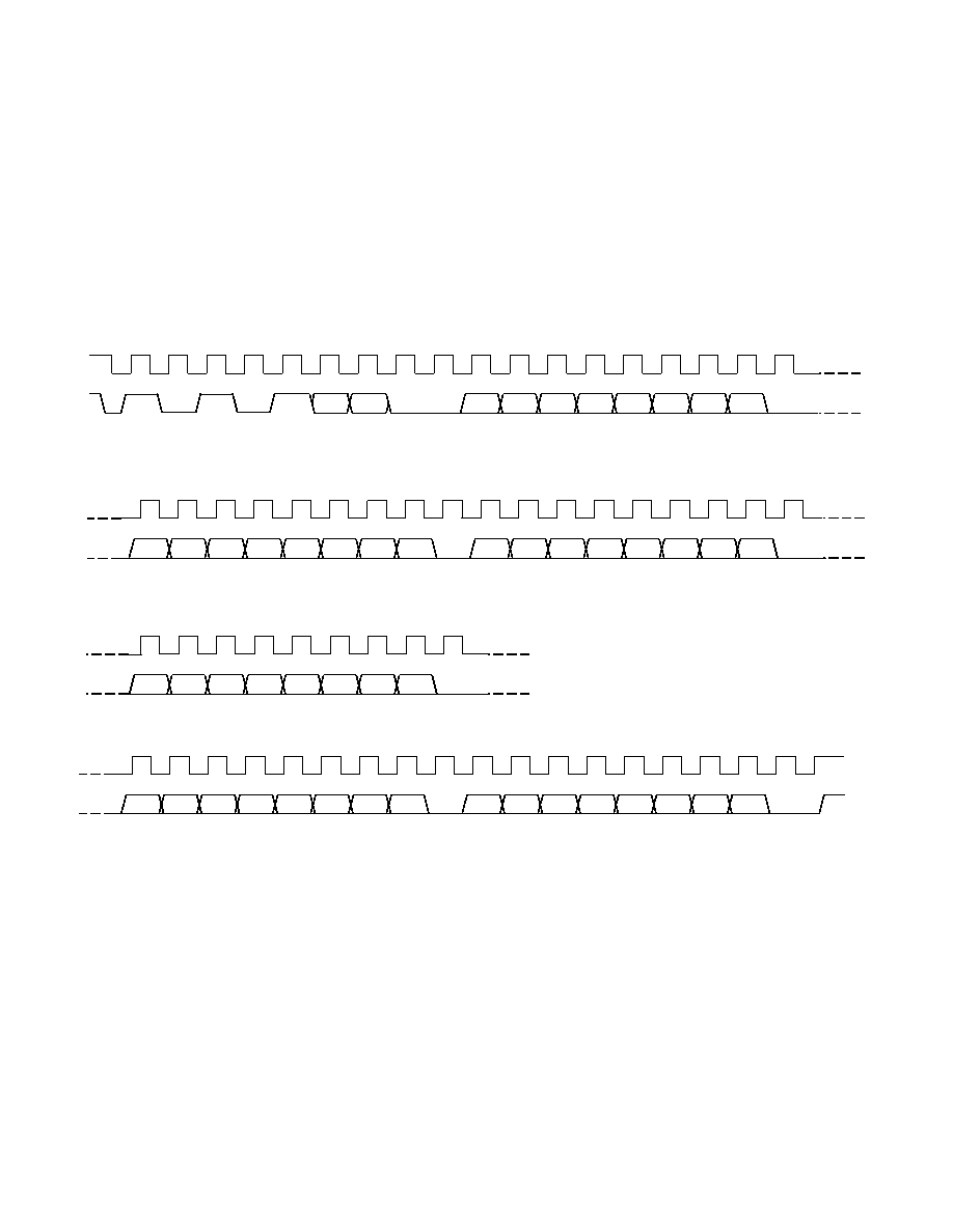
PRELIMINARY TECHNICAL DATA
REV. PrF 09/2003
2 6
AD5380
3-Byte Mode
Three byte mode allows the user update more than one channel in a write sequence without having to write the device
address byte each time. The device address byte is only required once and subsequent channel updates require the pointer
byte and the data bytes. In three byte mode the user begins with an address byte (R/
W = 0) after which the DAC will
acknowledge that it is prepared to receive data by pulling SDA low. The address byte is followed by the pointer
byte, this addresses the specific channel in the DAC to be addressed and is also acknowledged by the DAC. This is
then followed by the two data bytes. REG1 and REG0 determine the register to be updated.
If a STOP condition is not sent following the data bytes another channel can be updated by sending a new pointer
byte followed by the data bytes. This mode only requires 3-bytes to be sent to update any channel once the device
has been initially addressed and reduces the software overhead in updating the AD5380 channels. A STOP condition
at any time exits this mode. Figure 12 shows a typical configuration.
Figure 12 . 3-Byte AD5380, I2C Write Operation
0
A0
ACK
BY
AD538X
MSB
POINTER BYTE FOR CHANNEL "N"
A5
A4
A3
A2
A1
0
MOST SIGNIFICANT DATA BYTE
LEAST SIGNIFICANT DATA BYTE
SCL
SDA
REG1
LSB
MSB
LSB
ACK
BY
AD538X
ACK
BY
AD538X
REG0
MSB
1
0
1
0
1
AD0
R/
W
ACK
BY
AD538X
ADDRESS BYTE
START
COND
BY
MASTER
SCL
SDA
AD1
0
A0
ACK
BY
AD538X
MSB
A5
A4
A3
A2
A1
0
MOST SIGNIFICANT DATA BYTE
LEAST SIGNIFICANT DATA BYTE
SCL
SDA
REG1
LSB
MSB
LSB
ACK
BY
AD538X
ACK
BY
AD538X
STOP
COND
BY
MASTER
REG0
MSB
SCL
SDA
DATA FOR CHANNEL "N"
POINTER BYTE FOR CHANNEL "NEXT CHANNEL"
DATA FOR CHANNEL "NEXT CHANNEL"
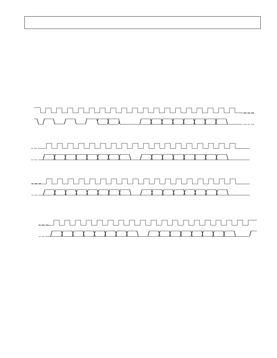
PRELIMINARY TECHNICAL DATA
REV. PrF 09/2003
AD5380
2 7
Figure 13 . 2-Byte AD5380, I2C Write Operation
2-Byte Mode
Two byte mode allows the user update channels sequentially following initialization of this mode. The device address
byte is only required once and the pointer address pointer is configured for auto increment or burst mode.
The user must begin with an address byte (R/
W = 0) after which the DAC will acknowledge that it is prepared to
receive data by pulling SDA low. The address byte is followed by a specific pointer byte (FF Hex) which initiates
the burst mode of operation. The address pointer initializes to channel zero and the data following the pointer is
loaded to channel 0, the address pointer automatically increments to the next address.
The REG0 and REG 1 bits in the data byte determine the register to be updated. In this mode, following the initial-
ization only the 2-data bytes are required to update a channel, the channel address automatically increments from
address 0 to channel 39 and then returns to the normal 3-byte mode of operation. This mode allows transmission of
data to all channels in one block and reduces the software overhead in configuring all channels. A STOP condition at any
time exits this mode. Toggle mode of operation is not supported in 2-Byte Mode. Figure 13 shows a typical configura-
tion.
A7=1
MOST SIGNIFICANT DATA BYTE
LEAST SIGNIFICANT DATA BYTE
SCL
SDA
REG1
LSB
MSB
LSB
ACK
BY
AD538X
ACK
BY
AD538X
REG0
MSB
CHANNEL 0 DATA
1
0
1
0
1
AD0
R/
W
A0=1
ACK
BY
Converter
ACK
BY
Converter
MSB
ADDRESS BYTE
START
COND
BY
MASTER
SCL
SDA
POINTER BYTE
AD1
A5=1
A4=1
A3=1
A2=1
A1=1
MOST SIGNIFICANT DATA BYTE
LEAST SIGNIFICANT DATA BYTE
SCL
SDA
REG1
LSB
MSB
LSB
ACK
BY
Converter
ACK
BY
Converter
STOP
COND
BY
MASTER
REG0
MSB
MOST SIGNIFICANT DATA BYTE
LEAST SIGNIFICANT DATA BYTE
SCL
SDA
REG1
LSB
MSB
LSB
ACK
BY
Converter
ACK
BY
Converter
REG0
MSB
CHANNEL 1 DATA
CHANNEL N DATA FOLLOWED BY STOP
A6=1
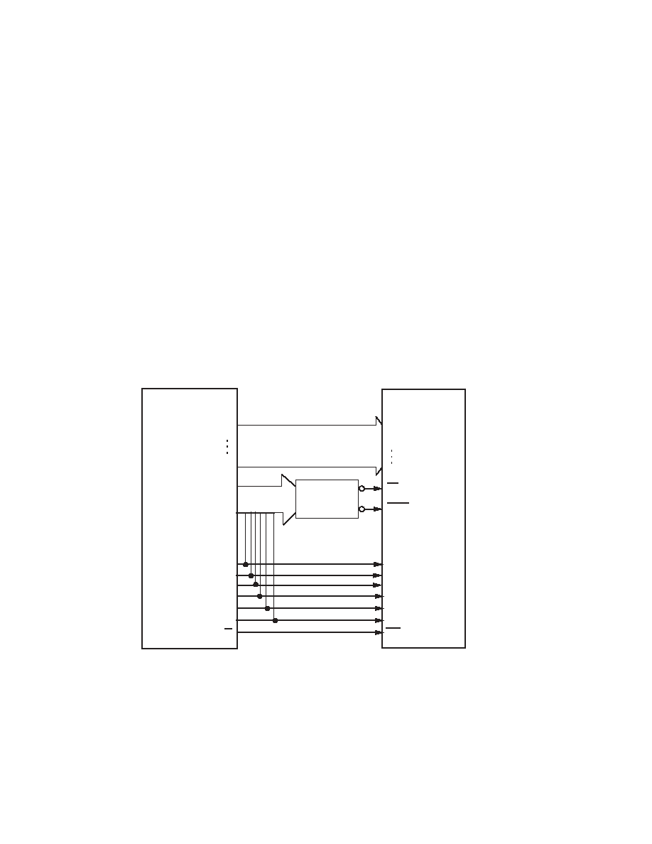
PRELIMINARY TECHNICAL DATA
REV. PrF 09/2003
2 8
AD5380
AD538X
CONTROLLER/
DSP PROCESSOR*
ADDRESS
DECODE
D15
D0
DATA
BUS
UPPER BITS OF
ADDRESS BUS
A2
A1
A0
R/W
*ADDITIONAL PINS OMITTED FOR CLARITY
D13
D0
CS
LDAC
A2
A1
A0
WR
A3
A4
A5
REG1
REG0
A3
A4
A5
AD5380 PARALLEL INTERFACE
The SER/
PAR pin must be tied low to enable the parallel interface and disable the serial interfaces. Figure 5 shows the
timing diagram for a parallel write. The parallel interface is controlled by the following pins:
CS
CS
CS
CS
CS Pin
Active low device select pin.
WR
WR
WR
WR
WR Pin
On the rising edge of
WR , with CS low, the address on pins A5-A0 are latched and data present on the data bus is
loaded into the selected input registers.
REG0, REG1 Pins
The REG0 and REG1 pins determine the destination register of the data being written to the AD5380. See Table I.
A5-A0 Pins
Each of the 40 DAC channels can be addressed individually.
DB13-DB0 Pins
The AD5380 accepts a straight 14-bit parallel word on DB13-DB0 where DB13 is the MSB and DB0 is the LSB.
MICROPROCESSOR INTERFACING
Parallel Interface
Figure 14 . AD5380 -Parallel Interface
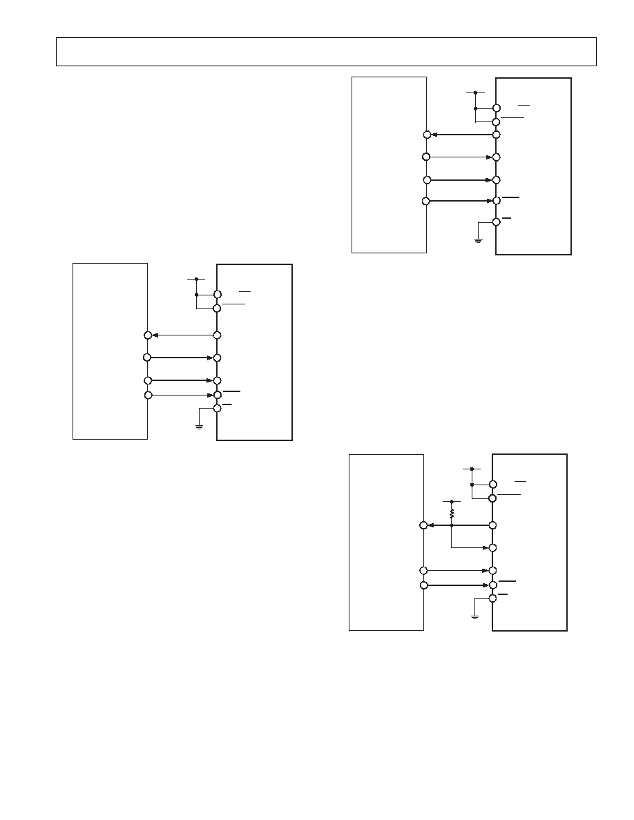
PRELIMINARY TECHNICAL DATA
REV. PrF 09/2003
AD5380
2 9
The AD5380 can be interfaced to a variety of 16-bit
microcontrollersor DSP processors. Figure 14 shows the
AD5380 family interfaced to a generic 16-bit
microcontroller/DSP processor. The lower address lines
from the processor are connected to A0 to A5 on the
AD5380 as shown. The upper address lines are decoded to
provide a CS,
LDAC
signals for the AD5380. The fast
interface timing of the AD5380 allows direct interface to a
wide variety of microcontrollers and DSPs as shown in
Figure 14.
AD5380 to MC68HC11
The Serial Peripheral Interface (SPI) on the MC68HC11
is configured for Master Mode (MSTR = 1), Clock Po-
larity Bit (CPOL) = 0 and the Clock Phase Bit (CPHA)
= 1. The SPI is configured by writing to the SPI Control
Register (SPCR)--see
68HC11 User Manual
. SCK of
the 68HC11 drives the SCLK of the AD5380, the MOSI
output drives the serial data line (D
IN
) of the AD5380 and
the MISO input is driven from D
OUT
. The
SYNC
signal is
derived from a port line (PC7). When data is being
transmitted to the AD5380, the
SYNC
line is taken low
(PC7). Data appearing on the MOSI output is valid on the
falling edge of SCK. Serial data from the 68HC11 is
transmitted in 8-bit bytes with only eight falling clock
edges occurring in the transmit cycle.
AD5380 to PIC16C6x/7x
The PIC16C6x/7x Synchronous Serial Port (SSP) is
configured as an SPI Master with the Clock Polarity bit =
0. This is done by writing to the Synchronous Serial Port
Control Register(SSPCON). See user
PIC16/17 Mi-
crocontroller User Manual
. In this example I/O
port RA1 is being used to pulse
SYNC
and enable the
serial port of the AD5380. This microcontroller
transfers only eight bits of data during each serial transfer
operation; therefore, three consecutive read/write opera-
tions are needed depending on the mode. Figure 16 shows
the connection diagram.
MISO
SCK
MC68HC11
RESET
SCLK
SDO
DIN
SYNC
AD538X
DV
DD
SPI/I2C
PC7
SER/PAR
MOSI
Figure 15 . AD5380 -MC68HC11 Interface
SCK/RC3
PIC16C6X/7X
RESET
SCLK
SDO
DIN
SYNC
AD538X
DV
DD
SPI/I2C
RA1
SER/PAR
SDO/RC5
SDI/RC4
Figure 16 . AD5380 -PIC16C6X/7X Interface
RxD
TxD
8XC51
RESET
SCLK
SDO
DIN
SYNC
AD538X
DV
DD
DV
DD
SPI/I2C
P1.1
SER/PAR
Figure 17 . AD5380 - 8051 Interface
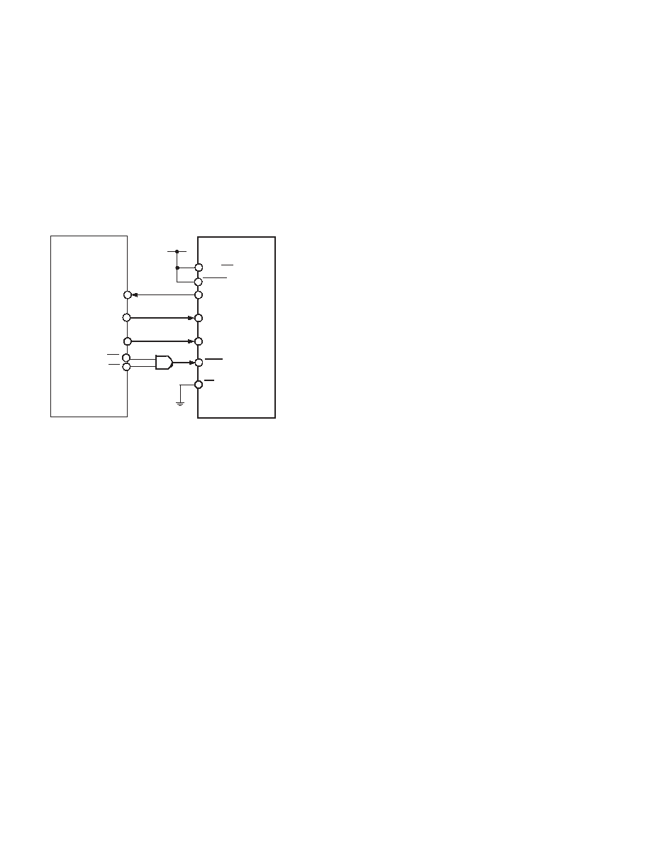
PRELIMINARY TECHNICAL DATA
REV. PrF 09/2003
3 0
AD5380
AD5380 to 8051
The AD5380 requires a clock synchronized to the serial
data. The 8051 serial interface must therefore be operated
in Mode 0. In this mode serial data enters and exits
through RxD and a shift clock is output on TxD. Figure
17 shows how the 8051 is connected to the AD5380. Be-
cause the AD5380 shifts data out on the rising edge of
the shift clock and latches data in on the falling edge,
the shift clock must be inverted. The AD5380 requires
its data with the MSB first. Since the 8051 outputs the
LSB first, the transmit routine must take this into account.
AD5380 to ADSP2101/2103
Figure 18 shows a serial interface between the AD5380
and the ADSP-2101/ADSP-2103. The ADSP-2101/
ADSP-2103 should be set up to operate in the SPORT
Transmit Alternate Framing Mode. The ADSP-2101/
ADSP-2103 SPORT is programmed through the SPORT
control register and should be configured as follows: Inter-
nal Clock Operation, Active Low Framing, 16-Bit Word
Length. Transmission is initiated by writing a word to the
Tx register after the SPORT has been enabled.
POWER SUPPLY DECOUPLING
In any circuit where accuracy is important, careful consid-
eration of the power supply and ground return layout
helps to ensure the rated performance. The printed circuit
board on which the AD5380 is mounted should be de-
signed so that the analog and digital sections are
separated, and confined to certain areas of the board. If
the AD5380 is in a system where multiple devices require
an AGND-to-DGND connection, the connection should
be made at one point only. The star ground point
should be established as close as possible to the device.
For supplies with multiple pins (AV
DD
, AV
CC
) it is recom-
mended to tie those pins together. The AD5380 should
have ample supply bypassing of 10 µF in parallel with
0.1 µF on each supply located as close to the package as
possible, ideally right up against the device. The 10 µF
capacitors are the tantalum bead type. The 0.1 µF capacitor
should have low Effective Series Resistance (ESR) and Ef-
fective Series Inductance (ESI), like the common
ceramic types that provide a low impedance path to
ground at high frequencies, to handle transient currents
due to internal logic switching.
The power supply lines of the AD5380 should use as large a
trace as possible to provide low impedance paths and
reduce the effects of glitches on the power supply line. Fast
switching signals such as clocks should be shielded with
digital ground to avoid radiating noise to other parts of
the board, and should never be run near the reference
inputs. A ground line routed between the D
IN
and SCLK
lines will help reduce crosstalk between them (not required
on a multilayer board as there will be a separate ground
plane, but separating the lines will help). It is essential to
minimize noise on V
IN
and REFIN lines.
Avoid crossover of digital and analog signals. Traces on
opposite sides of the board should run at right angles to
each other. This reduces the effects of feedthrough through
the board. A microstrip technique is by far the best, but not
always possible with a double-sided board. In this tech-
nique, the component side of the board is dedicated to
ground plane while signal traces are placed on the solder
side.
DR
SCK
ADSP2101/
ADSP2103
RESET
SCLK
SDO
DIN
SYNC
AD538X
DV
DD
SPI/I2C
RFS
SER/PAR
DT
TFS
Figure 18 . AD5380 -ADSP2101/ADSP3103 Interface
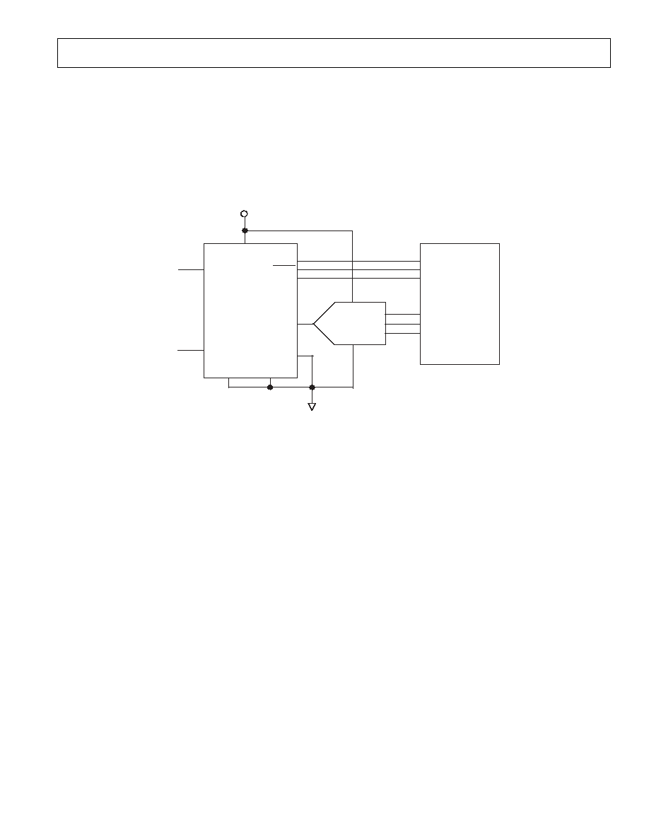
PRELIMINARY TECHNICAL DATA
REV. PrF 09/2003
AD5380
3 1
APPLICATIONS INFORMATION
AD5380 Monitor Function
The AD5380 contains a channel monitor function consisting of a multiplexer addressed via the interface allowing any
channel output to be routed to this pin for monitoring using an external ADC. In channel monitor mode Vout 39 be-
comes the MON_OUT pin, the pin to which all monitored signals are routed. The channel monitor function must be
enabled in the control register before any channels are routed to the MON_OUT pin. Table X contains the decoding
information required to route any channel to the MON_OUT pin. Selecting channel address 63 tristates the
MON_OUT pin. Figure 19 shows a typical monitoring circuit implemented using a 12-bit SAR ADC in a 6-lead sot
package. The controller output port selects the channel to be monitored and the input port reads the converted data from
the ADC.
AD5380
VOUT 39/MON_OUT
SCLK
SDATA
CS
AD7476
.
.
.
.
.
.
VOUT 0
VOUT 38
AVCC
VIN
AVCC
DAC_GND SIGNAL GND
AGND
DIN
SYNC
SCLK
CONTROLLER
INPUT PORT
OUTPUT PORT
GND
Figure 19. Typical Channel Monitoring Circuit
Toggle Mode Function
The toggle mode function allows an output signal to be generated using the
LDAC control signal that switches between
two DAC data registers. This function is configured using the SFR control register as follows. A write with
REG1=REG0=0, A5-A0=001100 specifies a control register write. The toggle mode function is enabled in groups of 8-
channels using bits CR6 to CR2 in the control register. See AD5380 control register description. Figure 20 shows a
block diagram of the toggle mode implementation. Each of the 40 DAC channels on the AD5380 contain an A and a B
data register. Note, the "B" registers can only be loaded when Toggle mode is enabled. The sequence of events when
configuring the AD5380 for toggle mode of operation is as follows:
i) Enable Toggle Mode for the required channels via the Control Register
ii) Load Data to A registers
iii) Load Data to B registers.
iv) Apply
LDAC.
The
LDAC is used to switch between the "A" and "B" registers in determining the analog output. The first LDAC
configures the output to reflect the data in the "A" registers. This mode offers significant advantages if the user wants to
generate a square wave at the output of all 40 channels as might be required to drive a liquid crystal based variable opti-
cal attenuators. In this case the user writes to the control register and enables the toggle function by setting CR6 to
CR2=1 enabling the five groups of 8 for toggle mode operation. The user must then load data to all 40 "A" registers
and "B" registers. Toggling the
LDAC will set the output values to reflect the data in the A and B registers and the
frequency of the
LDAC will determine the frequency of the squarewave output.
Toggle mode is disabled via the control register, the first LDAC following the disabling of the toggle mode will update
the outputs with the data contained in the "A" registers.
PRELIMINARY TECHNICAL DATA
REV. PrF 09/2003
3 2
AD5380
Thermal Monitor Function
The AD5380 contains a temperature shutdown function to protect the chip in case multiple outputs are shorted. The
short circuit current of each output amplifier is typically 40mA. Operating the AD5380 at 5V leads to a power dissipa-
tion of 200mW / shorted amplifier. With 5 channels shorted this leads to an extra watt of power dissipation. For the
100-lead LQFP the Qja is typically 44
°C
/W.
The thermal monitor is enabled by the user via CR8 in the control register. The output amplifiers on the AD5380 are
automatically powered down if the die temperature exceeds 130
°C
approx. After a thermal shutdown has occured the user
can re-enable the part by executing a soft power up if the temperature has dropped below 130
°C
or by turning off the
thermal monitor function via the control register.
INPUT
REGISTER
DATA
REGISTER
A
DAC
REGISTER
14-BIT DAC
LDAC
CONTROL INPUT
DATA
REGISTER
B
VOUT
INPUT
DATA
A/B
Figure 20. Toggle Mode Function
AD5380 in a MEMS Based Optical Optical Switch
MEMS based optical switches have a requirement for high resolution DACs in their feedforward control path that offer
high channel density with 14-bit monotonic behaviour. The AD5380, 40-channel, 14-bit DAC in a 100lead LQFP pack-
age satisifies these requirements. In the circuit shown in Figure 19, the 0V5V outputs of the AD5380 are amplified to
achieve an output range of 0V200V used to control actuators that determine the position of MEMS mirrors in an optical
switch. The exact position of each mirror is measured using sensors. The sensor outputs are multiplexed into a high reso-
lution ADC in determining the mirror position. The control loop is closed and driven by an ADSP-21065L, a 32-bit
SHARC
®
DSP with an SPI-compatible SPORT interface. It writes data to the DAC, controls the multiplexer, and reads
data from the ADC via the serial interface.
14-B it D A C
VO 1
A ctuators
For
M EM S
M irror
A rray
Sensor
+
M ultiplexer
8-C hannel A D C
(A D 7856)
A D 5380
14-B it D A C
VO 40
.
.
.
.
.
.
.
.
A D SP21065L
R EFIN
O utput R ange
0-200V
O R
Single C hannel
A D C (A D 7671)
+5V
A VD D
R EFO U T
.
.
.
.
G =50
G =50
0.01uF
Figure 19 . AD5380 in a MEMS based Optical Switch
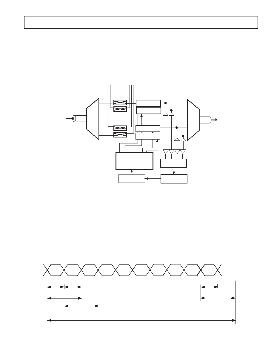
PRELIMINARY TECHNICAL DATA
REV. PrF 09/2003
AD5380
3 3
FIB R E
A D 5380,
40-C hannel,
14-B it D A C
D W D M
IN
D W D M
O U T
FIB R E
A D D
PO R TS
D R O P
PO R TS
FIB R E
A ttenuator
A ttenuator
A ttenuator
A ttenuator
AW G
AW G
.
.
.
.
.
.
.
.
.
N :1 M ultiplexer
TIA /LO G A M P
(A D 8304/5)
16-B IT A D C
Photo-diodes
C O N TR O LLER
l
l
l
l
1
2
n-1
n
.
.
.
. . . .
. . . .
O ptical
Sw itch
A D G 731
(40:1 M U X)
A D 7671
(0-5V, 1M SPS)
Figure 20 . OADM using the AD5380 as part of an Optical Attenuator
Optical Attenuators
The AD5380 based on its high channel count, high resolution, monotonic behaviour and high level of integration is ide-
ally targetted at optical attenuation applications used in dynamc gain equilizers, variable optical attenuators (VOA) and
Optical Add-Drop Mutliplexers (OADM). In these applications each wavelength is individually extracted using an ar-
rayed wavequide and its power monitored using a photo-diode, transimpedance amplifier and ADC in a close loop
control system. The AD5380 controls the optical attenuator for each wavelength ensuring that the power is equilized in
all wavelengths before being multiplexed onto the fibre. This prevents information loss and saturation from occurring at
amplification stages further along the fibre.
Utilizing the AD5380 FIFO
The AD5380 FIFO mode optimizes total system update rate in applications where a large number of channels need to be
updated. FIFO mode is only available when the parallel interface mode is selected. The FIFOEN pin is used to enable
the FIFO. The status of the FIFOEN pin is sampled during the initialisation sequence, therefore the FIFO status can
only be changed by resetting the device. An example of where a large number of channels need to be updated in a short
period of time would be in a telescope that provides for the cancellation of atmospheric distortion. In these systems as
many as 400channels need to be updated in a window of 40us. 400 channels necessitates the use of 10* AD5380 devices.
With FIFO mode enabled the data write cycle time is 40ns, therefore each group consisting of 40 channels can be fully
loaded 1.6us. In FIFO mode a complete group of 40 channels will update in 14.4us. Therefore the time taken to update
all 400channels will equate to 14.4us +9*1.6us = 28.8us. Figure 21 shows a graphical view of the FIFO operation
scheme.
GROUP A
Chnls 0-39
GROUP B
Chnls 40-79
GROUP C
Chnls 80-119
GROUP D
Chnls 120-159
GROUP E
Chnls 160-199
GROUP F
Chnls 200-239
GROUP H
Chnls 280-319
GROUP G
Chnls 240-279
GROUP I
Chnls 320-359
Time to Update 400 Channels = 28.8us
GROUP J
Chnls 360-399
1.6us
14.4us
FIFO DATA LOAD
Group B
1.6us
FIFO DATA LOAD
Group A
Output Update
Time for Group A
Output Update
Time for Group B
14.4us
FIFO DATA LOAD
Group J
1.6us
Output Update
Time for Group J
14.4us
Figure 21. Using FIFO mode 400 Channels Updated in under 30us.
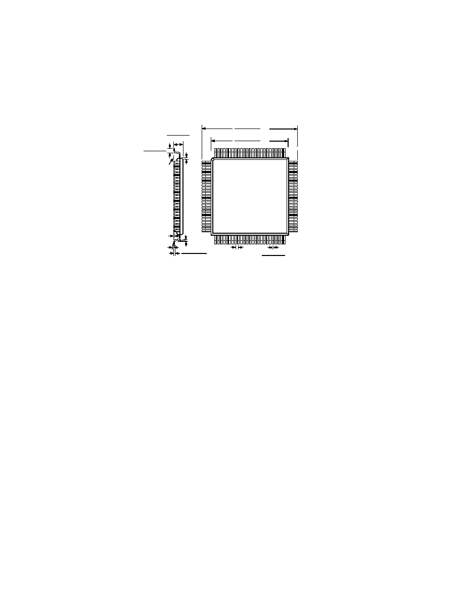
PRELIMINARY TECHNICAL DATA
REV. PrF 09/2003
3 4
AD5380
SEA TING
PLAN E
0.026 (0.65)
0.014 (0.35)
0.061 (1.55)
0.049 (1.25)
12¡
TYP
0.007 (0.177)
0.003 (0.077)
6¡ ± 4¡
0¡ Ð 10¡
0.004
(0.102)
MAX LEAD
COPLANARITY
TOP V IEW
(P IN S DO W N )
1
25
26
51
50
75
100
76
0.012 (0.20)
0.004 (0.10)
0.640 (16.25)
0.620 (15.75)
SQ
0.555 (14.10)
0.547 (13.90)
SQ
0.020 (0.50)
BSC
OUTLINE DIMENSIONS
ST100 (100 Lead LQFP) Package Dimensions